

mikrocont / 741
.pdfUA741
GENERAL PURPOSE SINGLE OPERATIONAL AMPLIFIER
■LARGE INPUT VOLTAGE RANGE
■NO LATCH-UP
■HIGH GAIN
■SHORT-CIRCUIT PROTECTION
■NO FREQUENCY COMPENSATION
■REQUIRED
■SAME PIN CONFIGURATION AS THE UA709
DESCRIPTION
The UA741 is a high performance monolithic operational amplifier constructed on a single silicon chip. It is intented for a wide range of analog applications.
■Summing amplifier
■Voltage follower
■Integrator
■Active filter
■Function generator
The high gain and wide range of operating voltages provide superior performances in integrator, summing amplifier and general feedback applications. The internal compensation network (6dB/ octave) insures stability in closed loop circuits.
PIN CONNECTIONS (top view)
N
DIP8
(Plastic Package)
D
SO8
(Plastic Micropackage)
ORDER CODE
Part Number |
Temperature Range |
Package |
||
|
|
|||
N |
D |
|||
|
|
|||
|
|
|
|
|
UA741C |
0°C, +70°C |
∙ |
∙ |
|
UA741I |
-40°C, +105°C |
∙ |
∙ |
|
|
|
|
|
|
UA741M |
-55°C, +125°C |
∙ |
∙ |
|
|
|
|
|
|
Example : UA741CN
N = Dual in Line Package (DIP)
D = Small Outline Package (SO) - also available in Tape & Reel (DT)
1 |
8 |
2 |
7 |
3 |
6 |
4 |
5 |
1 - Offset null 1
2 - Inverting input
3 - Non-inverting input
4- VCC-
5- Offset null 2
6- Output
7- VCC+
8- N.C.
November 2001 |
1/5 |

UA741
SCHEMATIC DIAGRAM
Non-Inverting input
|
|
|
|
|
Vcc+ |
|
Q8 |
Q9 |
Q12 |
Q13 |
|
|
Inverting |
|
R7 |
Q14 |
|
|
|
input |
|
|
|
|
|
|
4.5kΩ |
|
|
Q1 |
Q2 |
|
|
|
|
|
|
C1 |
|
||
|
|
|
|
30pF |
|
|
|
|
|
Q18 |
Q15 |
Q3 |
Q4 |
|
R5 |
R8 |
R9 |
|
39kΩ |
||||
|
7.5kΩ |
25Ω |
|||
|
|
|
|
||
|
|
|
|
|
Output |
|
|
|
|
|
R10 |
|
|
|
|
|
50Ω |
|
|
|
|
Q16 |
|
|
Q7 |
|
|
Q17 |
|
|
|
|
|
|
|
|
|
|
|
|
Q20 |
Q5 |
Q6 |
Q10 |
Q11 |
Q22 |
|
Offset null 1
R3
50kΩ
R1 |
R2 |
R4 |
R12 |
R11 |
1kΩ |
1kΩ |
5kΩ |
50kΩ |
50Ω |

 Vcc-
Vcc-
Offset
null 2
ABSOLUTE MAXIMUM RATINGS
Symbol |
Parameter |
UA741M |
UA741I |
UA741C |
Unit |
|
|
|
|
|
|
VCC |
Supply voltage |
|
±22 |
|
V |
Vid |
Differential Input Voltage |
|
±30 |
|
V |
Vi |
Input Voltage |
|
±15 |
|
V |
Ptot |
Power Dissipation 1) |
|
500 |
|
mW |
|
Output Short-circuit Duration |
|
Infinite |
|
|
|
|
|
|
|
|
Toper |
Operating Free-air Temperature Range |
-55 to +125 |
-40 to +105 |
0 to +70 |
°C |
Tstg |
Storage Temperature Range |
|
-65 to +150 |
|
°C |
1.Power dissipation must be considered to ensure maximum junction temperature (Tj) is not exceeded.
2/5

|
|
|
|
|
|
|
UA741 |
|
ELECTRICAL CHARACTERISTICS |
|
|
|
|
|
|
||
VCC = ±15V, Tamb = +25°C (unless otherwise specified) |
|
|
|
|
|
|||
Symbol |
|
Parameter |
|
Min. |
Typ. |
Max. |
Unit |
|
|
|
|
|
|
|
|
|
|
|
Input Offset Voltage (Rs ≤ 10kΩ) |
|
|
|
|
mV |
|
|
Vio |
Tamb = +25°C |
|
|
|
1 |
5 |
|
|
|
Tmin ≤ Tamb ≤ Tmax |
|
|
|
6 |
|
|
|
|
Input Offset Current |
|
|
|
|
|
nA |
|
Iio |
Tamb = +25°C |
|
|
|
2 |
30 |
|
|
|
Tmin ≤ Tamb ≤ Tmax |
|
|
|
70 |
|
|
|
|
Input Bias Current |
|
|
|
|
|
nA |
|
Iib |
Tamb = +25°C |
|
|
|
10 |
100 |
|
|
|
Tmin ≤ Tamb ≤ Tmax |
|
|
|
200 |
|
|
|
|
Large Signal Voltage Gain (Vo = ±10V, RL = 2kΩ) |
|
|
|
V/mV |
|
||
Avd |
Tamb = +25°C |
|
|
50 |
200 |
|
|
|
|
Tmin ≤ Tamb ≤ Tmax |
|
|
|
|
|||
|
|
25 |
|
|
|
|
||
|
Supply Voltage Rejection Ratio (Rs ≤ 10kΩ) |
|
|
|
|
dB |
|
|
SVR |
Tamb = +25°C |
|
|
77 |
90 |
|
|
|
|
Tmin ≤ Tamb ≤ Tmax |
|
77 |
|
|
|
|
|
|
Supply Current, no load |
|
|
|
|
mA |
|
|
ICC |
Tamb = +25°C |
|
|
1.7 |
2.8 |
|
|
|
|
Tmin ≤ Tamb |
≤ Tmax |
|
|
|
3.3 |
|
|
|
Input Common Mode Voltage Range |
|
|
|
|
V |
|
|
Vicm |
Tamb = +25°C |
|
|
±12 |
|
|
|
|
|
Tmin ≤ Tamb ≤ Tmax |
|
±12 |
|
|
|
|
|
|
Common Mode Rejection Ratio (RS ≤ 10kΩ) |
|
|
|
dB |
|
||
CMR |
Tamb = +25°C |
|
70 |
90 |
|
|
|
|
|
Tmin ≤ Tamb |
≤ Tmax |
|
70 |
|
|
|
|
IOS |
Output short Circuit Current |
|
10 |
25 |
40 |
mA |
|
|
|
Output Voltage Swing |
RL = 10kΩ |
|
|
|
V |
|
|
|
Tamb = +25°C |
|
|
|
|
|
||
|
|
12 |
14 |
|
|
|
||
±Vopp |
|
|
RL = 2kΩ |
10 |
13 |
|
|
|
|
Tmin ≤ Tamb ≤ Tmax |
RL = 10kΩ |
12 |
|
|
|
|
|
|
|
|
Ω |
10 |
|
|
|
|
|
|
|
RL = 2k |
|
|
|
|
|
SR |
Slew Rate |
|
|
|
|
|
V/μs |
|
Vi = ±10V, RL = 2kΩ, CL = 100pF, unity Gain |
0.25 |
0.5 |
|
|
|
|||
|
|
|
|
|||||
tr |
Rise Time |
|
|
|
|
|
μs |
|
Vi = ±20mV, RL = 2kΩ, CL = 100pF, unity Gain |
|
0.3 |
|
|
|
|||
|
|
|
|
|
||||
Kov |
Overshoot |
|
|
|
|
|
% |
|
Vi = 20mV, RL = 2kΩ, CL = 100pF, unity Gain |
|
5 |
|
|
|
|||
|
|
|
|
|
||||
Ri |
Input Resistance |
|
|
0.3 |
2 |
|
MΩ |
|
GBP |
Gain Bandwith Product |
|
|
|
|
MHz |
|
|
Vi = 10mV, RL = 2kΩ, CL = 100pF, f =100kHz |
0.7 |
1 |
|
|
|
|||
|
|
|
|
|||||
THD |
Total Harmonic Distortion |
|
|
|
|
% |
|
|
f = 1kHz, Av = 20dB, RL = 2kΩ, Vo = 2Vpp, CL = 100pF,Tamb = +25°C |
|
0.06 |
|
|
|
|||
|
|
|
|
|
||||
en |
Equivalent Input Noise Voltage |
|
|
|
|
nV |
|
|
f = 1kHz, Rs = 100Ω |
|
|
23 |
|
----------- |
|
||
|
|
|
|
Hz |
|
|||
|
|
|
|
|
|
|
|
|
m |
Phase Margin |
|
|
|
50 |
|
Degrees |
|
|
|
|
|
|
|
|
|
|
3/5
UA741
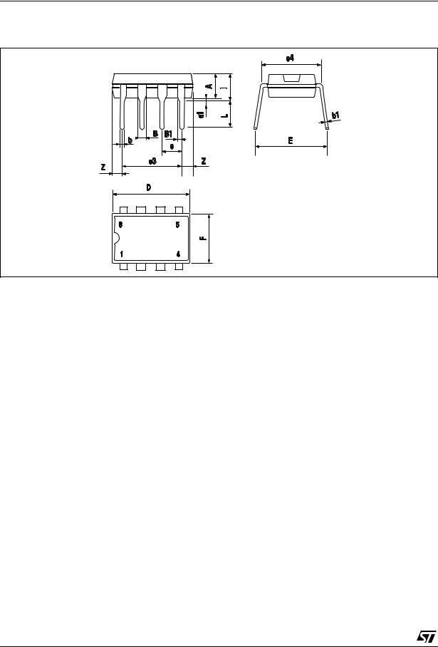
PACKAGE MECHANICAL DATA
8 PINS - PLASTIC DIP
Dim. |
|
Millimeters |
|
|
Inches |
|
|
|
|
|
|
|
|
||
Min. |
Typ. |
Max. |
Min. |
Typ. |
Max. |
||
|
|||||||
|
|
|
|
|
|
|
|
A |
|
3.32 |
|
|
0.131 |
|
|
a1 |
0.51 |
|
|
0.020 |
|
|
|
|
|
|
|
|
|
|
|
B |
1.15 |
|
1.65 |
0.045 |
|
0.065 |
|
|
|
|
|
|
|
|
|
b |
0.356 |
|
0.55 |
0.014 |
|
0.022 |
|
|
|
|
|
|
|
|
|
b1 |
0.204 |
|
0.304 |
0.008 |
|
0.012 |
|
|
|
|
|
|
|
|
|
D |
|
|
10.92 |
|
|
0.430 |
|
|
|
|
|
|
|
|
|
E |
7.95 |
|
9.75 |
0.313 |
|
0.384 |
|
|
|
|
|
|
|
|
|
e |
|
2.54 |
|
|
0.100 |
|
|
|
|
|
|
|
|
|
|
e3 |
|
7.62 |
|
|
0.300 |
|
|
|
|
|
|
|
|
|
|
e4 |
|
7.62 |
|
|
0.300 |
|
|
F |
|
|
6.6 |
|
|
0260 |
|
|
|
|
|
|
|
|
|
i |
|
|
5.08 |
|
|
0.200 |
|
|
|
|
|
|
|
|
|
L |
3.18 |
|
3.81 |
0.125 |
|
0.150 |
|
Z |
|
|
1.52 |
|
|
0.060 |
|
|
|
|
|
|
|
|
4/5
UA741
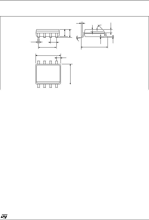
PACKAGE MECHANICAL DATA
8 PINS - PLASTIC MICROPACKAGE (SO)
|
L |
|
|
|
C |
c1 |
a3 |
|
|
||
a2 |
A |
|
|
b |
s |
a1 |
b1 |
|
e3 |
E |
|
|
|
|
D
M
8 |
5 |
|
F |
1 |
4 |
|
|
|
|
|
|
|
|
|
|
|
|
|
|
|
|
|
|
|
|
|
|
|
|
|
|
|
|
|
|
|
|
|
|
|
|
|
|
|
|
|
|
|
|
|
|
|
|
|
|
|
|
|
|
Dim. |
|
|
|
|
|
Millimeters |
|
|
|
|
Inches |
|
|||||
|
|
|
|
|
|
|
|
|
|
|
|
|
|
|
|
|
|
Min. |
|
|
|
Typ. |
Max. |
|
Min. |
Typ. |
Max. |
||||||||
|
|
|
|
|
|||||||||||||
|
|
|
|
|
|
|
|
|
|
|
|
|
|
|
|
|
|
A |
|
|
|
|
|
|
|
|
|
|
|
1.75 |
|
|
|
0.069 |
|
|
|
|
|
|
|
|
|
|
|
|
|
|
|
|
|
|
|
a1 |
0.1 |
|
|
|
|
|
|
|
|
|
|
0.25 |
|
0.004 |
|
0.010 |
|
|
|
|
|
|
|
|
|
|
|
|
|
|
|
|
|
|
|
a2 |
|
|
|
|
|
|
|
|
|
|
|
1.65 |
|
|
|
0.065 |
|
|
|
|
|
|
|
|
|
|
|
|
|
|
|
|
|
|
|
a3 |
0.65 |
|
|
|
|
|
|
|
|
|
|
0.85 |
|
0.026 |
|
0.033 |
|
|
|
|
|
|
|
|
|
|
|
|
|
|
|
|
|
|
|
b |
0.35 |
|
|
|
|
|
|
|
|
|
|
0.48 |
|
0.014 |
|
0.019 |
|
|
|
|
|
|
|
|
|
|
|
|
|
|
|
|
|
|
|
b1 |
0.19 |
|
|
|
|
|
|
|
|
|
|
0.25 |
|
0.007 |
|
0.010 |
|
C |
0.25 |
|
|
|
|
|
|
|
|
|
|
0.5 |
|
0.010 |
|
0.020 |
|
|
|
|
|
|
|
|
|
|
|
|
|
|
|
|
|
|
|
c1 |
|
|
|
|
|
|
|
|
|
|
|
|
|
45° (typ.) |
|
|
|
|
|
|
|
|
|
|
|
|
|
|
|
|
|
|
|
|
|
D |
4.8 |
|
|
|
|
|
|
|
|
|
|
5.0 |
|
0.189 |
|
0.197 |
|
|
|
|
|
|
|
|
|
|
|
|
|
|
|
|
|
|
|
E |
5.8 |
|
|
|
|
|
|
|
|
|
|
6.2 |
|
0.228 |
|
0.244 |
|
|
|
|
|
|
|
|
|
|
|
|
|
|
|
|
|
|
|
e |
|
|
|
1.27 |
|
|
|
|
|
|
0.050 |
|
|||||
|
|
|
|
|
|
|
|
|
|
|
|
|
|
|
|
|
|
e3 |
|
|
|
3.81 |
|
|
|
|
|
|
0.150 |
|
|||||
F |
3.8 |
|
|
|
|
|
|
|
|
|
|
4.0 |
|
0.150 |
|
0.157 |
|
|
|
|
|
|
|
|
|
|
|
|
|
|
|
|
|
|
|
L |
0.4 |
|
|
|
|
|
|
|
|
|
|
1.27 |
|
0.016 |
|
0.050 |
|
|
|
|
|
|
|
|
|
|
|
|
|
|
|
|
|
|
|
M |
|
|
|
|
|
|
|
|
|
|
|
0.6 |
|
|
|
0.024 |
|
S |
|
|
|
|
|
|
|
|
|
|
|
|
|
8° (max.) |
|
|
|
|
|
|
|
|
|
|
|
|
|
|
|
|
|
|
|
|
|
Information furnished is believed to be accurate and reliable. However, STMicroelectronics assumes no responsibility for the consequences of use of such information nor for any infringement of patents or other rights of third parties which may result from its use. No license is granted by implication or otherwise under any patent or patent rights of STMicroelectronics. Specifications mentioned in this publication are subject to change without notice. This publication supersedes and replaces all information previously supplied. STMicroelectronics products are not authorized for use as critical components in life support devices or systems without express written approval of STMicroelectronics.
©The ST logo is a registered trademark of STMicroelectronics
©2001 STMicroelectronics - Printed in Italy - All Rights Reserved
STMicroelectronics GROUP OF COMPANIES
Australia - Brazil - Canada - China - Finland - France - Germany - Hong Kong - India - Israel - Italy - Japan - Malaysia
Malta - Morocco - Singapore - Spain - Sweden - Switzerland - United Kingdom - United States
© http://www.st.com
5/5