

harris / CA3086
.PDFS E M I C O N D U C T O R
March 1993
CA3086
General Purpose N-P-N
Transistor Array
Applications |
Description |
•Three Isolated Transistors and One Differentially Connected Transistor Pair For Low-Power Applications from DC to 120 MHz
•General-Purpose Use in Signal Processing Systems Operating in the DC to 190MHz Range
•Temperature Compensated Amplifiers
•See Application Note, AN5296 “Application of the CA3018 Integrated-Circuit Transistor Array”' for Suggested Applications
The CA3086 consists of five general-purpose silicon n-p-n transistors on a common monolithic substrate. Two of the transistors are internally connected to form a differentially connected pair.
The transistors of the CA3086 are well suited to a wide variety of applications in low-power systems at frequencies from DC to 120MHz. They may be used as discrete transistors in conventional circuits. However, they also provide the very significant inherent advantages unique to integrated circuits, such as compactness, ease of physical handling and thermal matching.
Ordering Information
PART |
TEMPERATURE |
|
NUMBER |
RANGE |
PACKAGE |
|
|
|
CA3086 |
-55oC to +125oC |
14 Lead Plastic DIP |
|
|
|
CA3086M |
-55oC to +125oC |
14 Lead SOIC |
|
|
|
CA3086M96 |
-55oC to +125oC |
14 Lead SOIC* |
|
|
|
CA3086F |
-55oC to +125oC |
14 Lead Ceramic DIP |
|
|
|
* Denotes Tape and Reel
Pinout
CA3086
(PDIP, CDIP, SOIC)
TOP VIEW
1 |
|
|
|
14 |
|
2 |
|
|
Q5 |
13 |
SUBSTRATE |
|
|
|
|
|
|
3 |
Q1 |
|
|
12 |
|
Q2 |
|
|
|
||
|
|
|
|
|
|
4 |
|
|
|
11 |
|
5 |
|
|
Q4 |
10 |
|
|
|
|
|
|
|
6 |
|
|
|
9 |
|
7 |
|
Q3 |
|
8 |
|
|
|
|
|
|
CAUTION: These devices are sensitive to electrostatic discharge. Users should follow proper I.C. Handling Procedures. |
File Number 483.2 |
|
Copyright © Harris Corporation 1993
6-28

Specifications CA3086
Absolute Maximum Ratings |
|
Operating Conditions |
|
|
Power Dissipation |
|
|
Ambient Temperature Range |
-55oC to +125oC |
Any one transistor . . . . |
. . . . . . . . . . . . . . . . . . . . . . . . . . . |
300mW |
Operating. . . . . . . . . . . . . . . . . . . . . . . . . . . . . . . |
|
Total package up to T |
= +55oC . . . . . . . . . . . . . . . . . . . . |
750mW |
Storage . . . . . . . . . . . . . . . . . . . . . . . . . . . . . . . . |
-65oC to +150oC |
A |
Derate linearly 6.67 mW/oC |
|
|
|
Above T = +55oC. . . . |
|
|
||
A |
|
+175oC |
|
|
Junction Temperature . . . |
. . . . . . . . . . . . . . . . . . . . . . . . . . . |
|
|
|
Junction Temperature (Plastic Package) . . . . . . . . . . . . . . . |
+150oC |
|
|
|
Lead Temperature (Soldering 10 Sec.). . . . . . . . . . . . . . . . . |
+300oC |
|
|
|
The following ratings apply for each transistor in the device: |
|
|
|
|
Collector-to-Emitter Voltage, VCEO . . . . . . . . . . . . . . . . . . |
. . . 15V |
|
|
|
Collector-to-Base Voltage, VCBO . . . . . . . . . . . . . . . . . . . . . |
. . 20V |
|
|
|
Collector-to-Substrate Voltage, VCIO (Note 1). . . . . . . . . . . |
. . 20V |
|
|
|
Emitter-to-Base Voltage, VEBO . . . . . . . . . . . . . . . . . . . . . . |
. . . 5V |
|
|
|
Collector Current, IC . . |
. . . . . . . . . . . . . . . . . . . . . . . . . . . . |
. 50mA |
|
|
CAUTION: Stresses above those listed in “Absolute Maximum Ratings” may cause permanent damage to the device. This is a stress only rating and operation of the device at these or any other conditions above those indicated in the operational sections of this specification is not implied.
Electrical Specifications |
T = +25oC, For Equipment Design |
|
|
|
|
||
|
A |
|
|
|
|
|
|
|
|
|
|
|
|
|
|
|
|
|
TEST |
|
LIMITS |
|
|
|
|
|
|
|
|
|
|
PARAMETERS |
|
SYMBOLS |
CONDITIONS |
MIN |
TYP |
MAX |
UNITS |
|
|
|
|
|
|
|
|
Collector-to-Base Breakdown Voltage |
V(BR)CBO |
lC = 10μA, IE = 0 |
20 |
60 |
- |
V |
|
Collector-to-Emitter Breakdown Voltage |
V(BR)CEO |
IC = 1mA, IB = 0 |
15 |
24 |
- |
V |
|
Collector-to-Substrate Breakdown Voltage |
V(BR)ClO |
IC = 10μA, ICI = 0 |
20 |
60 |
- |
V |
|
Emitter-to-Base Breakdown Voltage |
V(BR)EBO |
IE = 10μA, IC = 0 |
5 |
7 |
- |
V |
|
Collector-Cutoff Current (Figure |
1) |
ICBO |
VCB = 10V, IE = 0, |
- |
0.002 |
100 |
nA |
Collector-Cutoff Current (Figure |
2) |
ICEO |
VCE = 10V, IB = 0, |
- |
(Figure 2) |
5 |
μA |
DC Forward-Current Transfer Ratio (Figure 3) |
hFE |
VCE = 3V, IC = 1mA |
40 |
100 |
- |
|
|
NOTE: |
|
|
|
|
|
|
|
1.The collector of each transistor in the CA3086 is isolated from the substrate by an integral diode. The substrate (terminal 13) must be connected to the most negative point in the external circuit to maintain isolation between transistors and to provide for normal transistor action. To avoid undesirable coupling between transistors, the substrate (terminal 13) should be maintained at either DC or signal (AC) ground. A suitable bypass capacitor can be used to establish a signal ground.
Electrical Specifications T = +25oC, Typical Values Intended Only for Design Guidance |
|
|
|||
A |
|
|
|
|
|
|
|
|
|
|
|
|
|
|
|
TYPICAL |
|
PARAMETERS |
SYMBOLS |
TEST CONDITIONS |
VALUES |
UNITS |
|
|
|
|
|
|
|
DC Forward-Current Transfer Ratio |
hFE |
VCE = 3V |
IC = 10mA |
100 |
|
(Figure 3) |
|
|
|
|
|
|
|
IC = 10μA |
54 |
|
|
|
|
|
|
||
|
|
|
|
|
|
Base-to-Emitter Voltage (Figure 4) |
VBE |
VCE = 3V |
IE = 1 mA |
0.715 |
V |
|
|
|
IE = 10mA |
0.800 |
V |
|
|
|
|
|
|
VBE Temperature Coefficient (Figure 5) |
VBE/ T |
VCE = 3V, lC = 1 mA |
|
-1.9 |
mV/oC |
|
|
|
|
|
|
Collector-to-Emitter |
VCE SAT |
IB = 1mA, IC = 10mA |
|
0.23 |
V |
Saturation Voltage |
|
|
|
|
|
|
|
|
|
|
|
Noise Figure (Low Frequency) |
NF |
f = 1kHz, VCE = 3V, IC = 100μA, |
3.25 |
dB |
|
|
|
RS = 1kΩ |
|
|
|
6-29
Specifications CA3086
Electrical Specifications T |
= +25oC, Typical Values Intended Only for Design Guidance (Continued) |
|
||||
|
A |
|
|
|
|
|
|
|
|
|
|
|
|
|
|
|
|
|
TYPICAL |
|
|
PARAMETERS |
|
SYMBOLS |
TEST CONDITIONS |
VALUES |
UNITS |
|
|
|
|
|
|
|
Low-Frequency, Small-Signal Equivalent- |
|
f = 1kHz,VCE = 3V, IC = 1mA |
|
|
||
Circuit Characteristics: |
|
|
|
|
|
|
|
Forward Current-Transfer Ratio |
|
hFE |
|
100 |
- |
|
(Figure 6) |
|
|
|
|
|
|
|
|
|
|
|
|
|
Short-Circuit Input Impedance |
|
hIE |
|
3.5 |
kΩ |
|
(Figure 6) |
|
|
|
|
|
|
|
|
|
|
|
|
|
Open-Circuit Output Impedance |
|
hOE |
|
15.6 |
μmho |
|
(Figure 6) |
|
|
|
|
|
|
|
|
|
|
|
|
|
Open-Circuit Reverse-Voltage |
|
h RE |
|
1.8 X 10⁻⁴ |
- |
|
Transfer Ratio (Figure 6) |
|
|
|
|
|
|
|
|
|
|
|
|
Admittance Characteristics: |
|
|
f = 1MHz,VCE = 3V, lC = 1mA |
|
|
|
|
Forward Transfer Admittance |
|
yFE |
|
31 - j1.5 |
mmho |
|
(Figure 7) |
|
|
|
|
|
|
|
|
|
|
|
|
|
Input Admittance (Figure 8) |
|
yIE |
|
0.3 + j0.04 |
mmho |
|
Output Admittance (Figure 9) |
|
yOE |
|
0.001 + j0.03 |
mmho |
|
Reverse Transfer Admittance |
|
yRE |
|
See Figure 10 |
- |
|
(Figure 10) |
|
|
|
|
|
|
|
|
|
|
|
|
Gain-Bandwidth Product (Figure 11) |
|
fT |
VCE = 3V, IC = 3mA |
550 |
MHz |
|
|
|
|
|
|
|
|
Emitter-to-Base Capacitance |
|
CEBO |
VEB = 3V, IE = 0 |
0.6 |
pF |
|
Collector-to-Base Capacitance |
|
CCBO |
VCB = 3V, IC = 0 |
0.58 |
pF |
|
Collector-to-Substrate Capacitance |
|
CClO |
VC l = 3V, IC = 0 |
2.8 |
pF |
|
|
|
|
|
|
|
|
Typical Static Characteristics for Each Transistor
|
102 |
IE = 0 |
|
|
|
|
|
|
|
|
|
|
|
(nA) |
10 |
|
VCB = 15V |
|
|
|
|
|
|
|
|||
CURRENT |
|
|
|
|
||
|
|
VCB = 10V |
|
|
|
|
1 |
|
VCB = 5V |
|
|
|
|
|
|
|
|
|
|
|
CUTOFF |
10-1 |
|
|
|
|
|
10-2 |
|
|
|
|
|
|
COLLECTOR |
|
|
|
|
|
|
10-3 |
|
|
|
|
|
|
|
|
|
|
|
|
|
|
10-4 |
|
|
|
|
|
|
0 |
25 |
50 |
75 |
100 |
125 |
TEMPERATURE (oC)
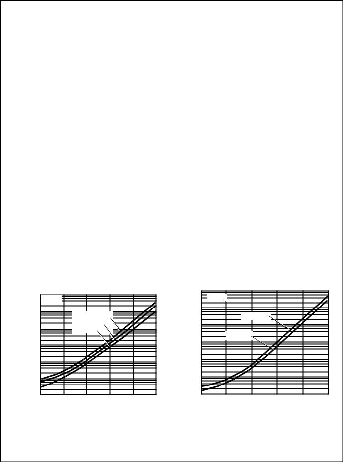
FIGURE 1. ICBO vs TEMPERATURE
|
103 |
IB = 0 |
|
|
|
|
(nA) |
|
|
|
|
|
|
102 |
|
|
|
|
|
|
CURRENT |
|
|
VCE = 10V |
|
|
|
10 |
|
|
|
|
|
|
|
|
VCE = 5V |
|
|
|
|
CUTOFF |
|
|
|
|
|
|
1 |
|
|
|
|
|
|
|
|
|
|
|
|
|
COLLECTOR |
10-1 |
|
|
|
|
|
10-2 |
|
|
|
|
|
|
|
|
|
|
|
|
|
|
10-3 |
|
|
|
|
|
|
0 |
25 |
50 |
75 |
100 |
125 |
AMBIENT TEMPERATURE (oC)
FIGURE 2. ICEO vs TEMPERATURE
6-30
CA3086
Typical Static Characteristics for Each Transistor (Continued)
120 |
|
|
|
|
|
VCE = 3V |
|
||||
|
|
||||
|
T |
= +25oC |
|
||
|
|
||||
110 |
A |
|
|
|
hFE |
|
|
|
|
||
FORWARDSTATICCURRENT TRANSFERRATIO (h |
|
) |
|
FE |
100 |
90
80
70
60
50
0.01 |
0.1 |
1 |
10 |
EMITTER CURRENT (mA)
|
|
|
|
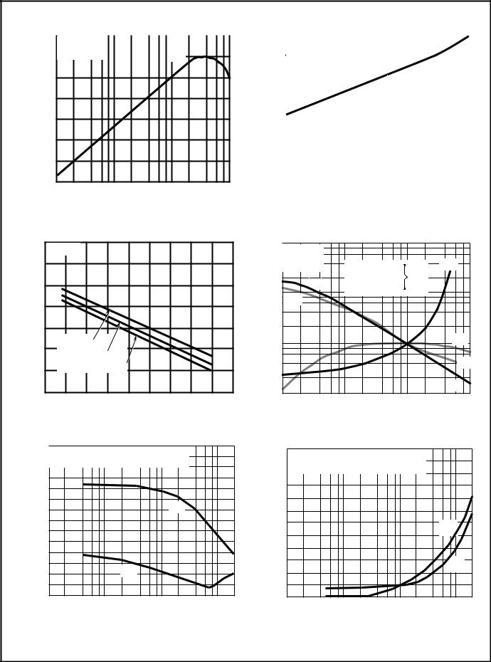
FIGURE 3. hFE vs IE |
|
|
|
||
|
VCB = 3V |
|
|
|
|
|
|
||
(V) |
|
|
|
|
|
|
|
|
|
VOLTAGE |
0.9 |
|
|
|
|
|
|
|
|
0.8 |
|
|
|
|
|
|
|
|
|
-EMITTER |
|
|
|
|
|
|
|
|
|
0.7 |
|
|
|
|
|
|
|
|
|
|
IE = 3mA |
|
|
|
|
|
|
||
-TO |
0.6 |
|
|
|
|
|
|
||
|
IE = 1mA |
|
|
|
|
|
|||
BASE |
|
|
|
|
|
|
|
||
0.5 |
|
|
IE = 0.5mA |
|
|
|
|
|
|
|
|
|
|
|
|
|
|
|
|
|
0.4 |
|
|
|
|
|
|
|
|
|
-75 |
-50 |
-25 |
0 |
25 |
50 |
75 |
100 |
125 |
|
|
|
AMBIENT TEMPERATURE (oC) |
|
|||||
FIGURE 5. VBE vs TEMPERATURE
) |
|
|
COMMON EMITTER CIRCUIT, BASE INPUT |
|
|||||
FE |
|
|
|
||||||
|
|
T |
= +25oC, V |
|
= 3V, I |
|
= 1mA |
|
|
(g |
|
|
CE |
C |
|
||||
(mmhos) |
40 |
A |
|
|
|
|
|||
|
|
|
|
|
|
|
|||
30 |
|
|
|
|
|
|
|
||
FORWARD TRANSFERCONDUCTANCE |
) |
|
|
|
|
|
|
|
|
FE |
|
|
|
|
|
|
gFE |
|
|
AND SUSCEPTANCE (b |
20 |
|
|
|
|
|
|
||
10 |
|
|
|
|
|
|
|
||
0 |
|
|
|
bFE |
|
||||
-10 |
|
|
|
|
|||||
-20 |
|
|
|
|
|
|
|
||
|
|
|
|
|
|
|
|
|
|
|
|
|
0.1 |
|
1 |
|
10 |
100 |
|
FREQUENCY (MHz)
FIGURE 7. yFE vs FREQUENCY
|
0.8 |
|
|
|
|
|
|
|
|
|
|
|
|
|
|
|
|
|
|
VCE = 3V |
|
|
|
|
|
|
|
|
|
|
|
|
|
||||
|
|
|
|
|
|
|
|
|
|
|
|
|
|
|
||||
|
|
TA = +25oC |
|
|
|
|
|
|
|
|
|
|
|
|
|
|||
(V) |
|
|
|
|
|
|
|
|
|
|
|
|
|
|
|
|
|
|
VOLTAGE |
0.7 |
|
|
|
|
|
|
|
|
|
|
|
|
|
|
|
|
|
|
|
|
|
|
|
|
|
|
|
|
|
|
|
|
|
|
|
|
|
|
|
|
|
|
|
|
|
|
VBE |
|
|
|
|
|
|||
EMITTER-TO- |
0.6 |
|
|
|
|
|
|
|
|
|
|
|
|
|
|
|
|
|
|
|
|
|
|
|
|
|
|
|
|
|
|
|
|
|
|
|
|
BASE |
0.5 |
|
|
|
|
|
|
|
|
|
|
|
|
|
|
|
|
|
|
|
|
|
|
|
|
|
|
|
|
|
|
|
|
|
|
||
|
|
|
|
|
|
|
|
|
|
|
|
|
|
|
|
|
|
|
|
0.4 |
|
|
|
|
|
|
|
|
|
|
|
|
|
|
|
|
|
|
|
|
|
|
|
|
|
|
|
|
|
|
|
|
|
|
|
|
|
0.01 |
|
|
|
0.1 |
1.0 |
10 |
|||||||||||
EMITTER CURRENT (mA)
FIGURE 4. VBE vs IE
|
100 |
VCE = 3V |
|
|
|
|
|
|
|
|
|
|
|
f = 1kHz |
|
|
|
PARAMETERSh |
|
TA = +25oC |
hFE = 100 |
|
hOE |
|
|
hIE = 3.5kΩ |
AT |
|
|
|
|
hIE |
hRE = 1.88 x 10⁻⁴ |
1mA |
|
|
10 |
hRE |
hOE = 15.6μmho |
|
|
|
|
|
|
||
NORMALIZED |
|
|
|
|
|
|
|
|
|
hRE |
|
|
1.0 |
|
|
|
hFE |
|
|
|
|
|
|
|
0.1 |
|
|
|
hIE |
|
0.01 |
0.1 |
1.0 |
10 |
|
|
|
|
COLLECTOR CURRENT (mA) |
|
|
|
|
FIGURE 6. NORMALIZED hFE, hIE, hRE, hOE vs IC |
|||||
|
|
6 |
COMMON EMITTER CIRCUIT, BASE INPUT |
||||
|
|
|
|||||
|
|
|
T |
= +25oC, V |
= 3V, I |
C |
= 1mA |
|
(mmhos) |
5 |
A |
CE |
|
|
|
) |
|
|
|
|
|
||
|
|
|
|
|
|
||
IE |
|
|
|
|
|
|
|
(g |
|
|
|
|
|
|
|
INPUT CONDUCTANCE |
) |
4 |
|
|
|
|
|
IE |
|
|
|
|
|
||
|
|
|
|
|
|
||
AND SUSCEPTANCE (b |
3 |
|
|
|
|
bIE |
|
|
|
|
|
|
|||
2 |
|
|
|
|
|
||
1 |
|
|
|
|
gIE |
||
|
|
|
|
|
|||
|
|
|
|
|
|
||
|
|
0 |
|
|
|
|
|
0.1 |
1 |
10 |
100 |
|
|
FREQUENCY (MHz) |
|
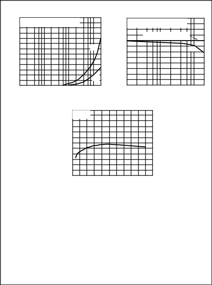
FIGURE 8. yIE vs FREQUENCY
6-31
CA3086
Typical Static Characteristics for Each Transistor (Continued)
|
|
COMMON EMITTER CIRCUIT, BASE INPUT |
|
|||||
|
|
6 |
= +25oC, V |
|
= 3V, I |
|
= 1mA |
|
|
|
T |
CE |
C |
|
|||
|
|
A |
|
|
|
|
||
) |
(mmhos) |
|
|
|
|
|
|
|
OE |
5 |
|
|
|
|
|
|
|
(g |
|
|
|
|
|
|
|
|
OUTPUT CONDUCTANCE |
) |
|
|
|
|
|
|
|
OE |
4 |
|
|
|
|
|
|
|
AND SUSCEPTANCE (b |
|
|
|
|
|
|
||
|
|
|
|
|
|
bOE |
||
3 |
|
|
|
|
|
|
||
2 |
|
|
|
|
|
|
||
1 |
|
|
|
|
|
gOE |
||
|
|
|
|
|
|
|
|
|
|
|
0 |
|
|
|
|
|
|
|
|
0.1 |
|
|
1 |
|
10 |
100 |
|
|
|
|
|
FREQUENCY (MHz) |
|
||
FIGURE 9. yOE vs FREQUENCY
) |
|
COMMON EMITTER CIRCUIT, BASE INPUT |
|
||||
RE |
|
T |
= +25oC, V |
= 3V, I |
C |
= 1m |
|
(g |
(mmhos) |
A |
CE |
|
|
|
|
|
gRE IS SMALL AT FREQUENCIES |
|
|||||
|
|
|
|
LESS THAN 500MHz |
|
||
REVERSE TRANSFERCONDUCTANCE |
) |
0 |
|
|
|
|
|
RE |
|
|
|
|
|
||
|
|
|
|
|
|
||
AND SUSCEPTANCE (b |
-0.5 |
|
|
|
|
bRE |
|
|
|
|
|
|
|||
-1.0 |
|
|
|
|
|
||
-1.5 |
|
|
|
|
|
||
-2.0 |
|
|
|
|
|
||
|
|
|
|
|
|
|
|
|
|
1 |
|
|
10 |
100 |
|
|
|
|
|
FREQUENCY (MHz) |
|
||
FIGURE 10. yRE vs FREQUENCY
GAIN BANDWIDTH PRODUCT (MHz)
VCE = 3V TA = +25oC
1000
900
800
700
600
500
400
300
200
100
0
0 |
1 |
2 |
3 |
4 |
5 |
6 |
7 |
8 |
9 |
10 |
COLLECTOR CURRENT (mA)
FIGURE 11. fT vs IC
6-32