
Курсовая / ICL7106, ICL7107
.pdf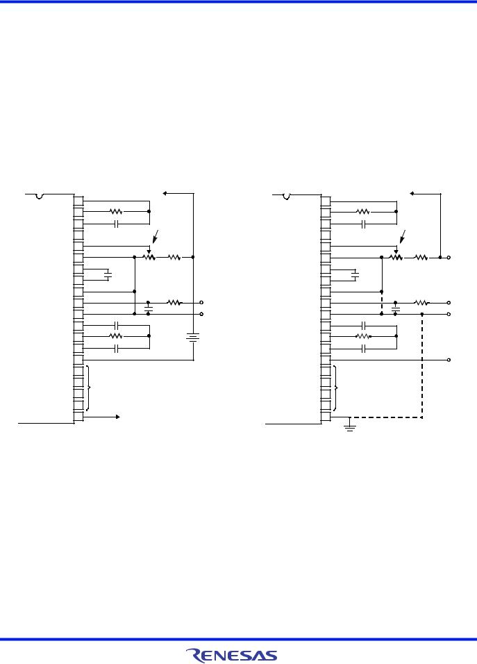
ICL7106, ICL7107, ICL7107S
Typical Applications
The ICL7106 and ICL7107 may be used in a wide variety of configurations. The circuits which follow show some of the possibilities, and serve to illustrate the exceptional versatility of these A/D converters.
The following application notes contain very useful information on understanding and applying this part and are available from Intersil Corporation.
Typical Applications
OSC 1 |
40 |
TO PIN 1 |
|
|
100kΩ |
|
|
||
OSC 2 |
39 |
|
|
|
|
|
|
||
OSC 3 |
38 |
100pF |
SET VREF |
|
TEST |
37 |
|
||
= 100mV |
|
|||
|
|
|||
REF HI |
36 |
|
|
|
REF LO |
35 |
1kΩ |
22kΩ |
|
CREF |
34 |
|
||
0.1µF |
|
|
||
CREF |
33 |
|
|
|
|
|
|
||
COMMON |
32 |
|
1MΩ |
+ |
IN HI |
31 |
|
0.01µF |
IN |
IN LO |
30 |
|
||
0.47µF |
|
- |
||
A-Z |
29 |
|
||
47kΩ |
|
+ |
||
BUFF |
28 |
|
||
|
-9V |
|||
|
|
|||
INT |
27 |
0.22µF |
|
|
V - |
26 |
|
|
|
|
|
|
||
G2 |
25 |
|
|
|
C3 |
24 |
TO DISPLAY |
|
|
A3 |
23 |
|
|
|
|
|
|
||
G3 |
22 |
|
|
|
BP |
21 |
TO BACKPLANE |
|
|
Values shown are for 200mV full scale, 3 readings/sec., floating supply voltage (9V battery).
FIGURE 11. ICL7106 USING THE INTERNAL REFERENCE
Application Notes
NOTE # |
DESCRIPTION |
|
|
AN016 |
“Selecting A/D Converters” |
|
|
AN017 |
“The Integrating A/D Converter” |
|
|
AN018 |
“Do’s and Don’ts of Applying A/D Converters” |
|
|
AN023 |
“Low Cost Digital Panel Meter Designs” |
|
|
AN046 |
“Building a Battery-Operated Auto Ranging DVM with the ICL7106” |
|
|
AN052 |
“Tips for Using Single Chip 31/2 Digit A/D Converters” |
AN9609 |
“Overcoming Common Mode Range Issues When Using Intersil |
|
Integrating Converters” |
|
|
OSC 1 |
40 |
TO PIN 1 |
|
|
100kΩ |
|
|
||
OSC 2 |
39 |
|
|
|
|
|
|
||
OSC 3 |
38 |
100pF |
SET VREF |
|
TEST |
37 |
|
||
= 100mV |
|
|||
|
|
|||
REF HI |
36 |
|
|
|
REF LO |
35 |
1kΩ |
22kΩ |
+5V |
CREF |
34 |
|
||
0.1µF |
|
|
||
CREF |
33 |
|
|
|
|
|
|
||
COMMON |
32 |
|
1MΩ |
+ |
IN HI |
31 |
|
0.01µF |
IN |
IN LO |
30 |
|
||
0.47µF |
|
- |
||
A-Z |
29 |
|
||
47kΩ |
|
|
||
BUFF |
28 |
|
|
|
|
|
|
||
INT |
27 |
0.22µF |
|
|
V - |
26 |
|
-5V |
|
|
|
|||
G2 |
25 |
|
|
|
C3 |
24 |
TO DISPLAY |
|
|
A3 |
23 |
|
|
|
|
|
|
||
G3 |
22 |
|
|
|
GND |
21 |
|
|
|
Values shown are for 200mV full scale, 3 readings/sec. IN LO may be tied to either COMMON for inputs floating with respect to supplies, or GND for single ended inputs. (See discussion in “Analog COMMON” on page 7.)
FIGURE 12. ICL7107 USING THE INTERNAL REFERENCE
FN3082 |
Rev 9.00 |
|
Page 11 of 17 |
October 24, 2014 |
|
|
|
|
|
||
|
|
||
ICL7106, ICL7107, ICL7107S |
|
|
|
|
|
|
|
||
Typical Applications (Continued) |
|
|
|
|
|
||||
OSC 1 |
40 |
TO PIN 1 |
|
OSC 1 |
40 |
TO PIN 1 |
|
||
100kΩ |
|
|
100kΩ |
|
|
||||
OSC 2 |
39 |
|
|
OSC 2 |
39 |
|
|
||
|
|
|
|
|
|
||||
OSC 3 |
38 |
100pF |
SET VREF |
OSC 3 |
38 |
100pF |
SET VREF |
|
|
TEST |
37 |
= 100mV |
|
TEST |
37 |
= 100mV |
|
||
|
|
|
|
||||||
REF HI |
36 |
|
|
|
REF HI |
36 |
|
|
|
REF LO |
35 |
|
|
V + |
REF LO |
35 |
|
|
+5V |
CREF |
34 |
1kΩ |
10kΩ |
10kΩ |
CREF |
34 |
1kΩ |
100kΩ |
|
0.1µF |
|
|
0.1µF |
|
6.8V |
||||
CREF |
33 |
1.2V (ICL8069) |
CREF |
33 |
|
||||
|
|
|
|
||||||
COMMON |
32 |
|
1MΩ |
+ |
COMMON |
32 |
|
1MΩ |
+ |
IN HI |
31 |
|
0.01µF |
IN |
IN HI |
31 |
|
0.01µF |
IN |
IN LO |
30 |
0.47µF |
IN LO |
30 |
|
||||
|
- |
0.47µF |
|
- |
|||||
A-Z |
29 |
|
A-Z |
29 |
|
||||
47kΩ |
|
|
47kΩ |
|
|
||||
BUFF |
28 |
|
|
BUFF |
28 |
|
|
||
|
|
|
|
|
|
||||
INT |
27 |
0.22µF |
V - |
INT |
27 |
0.22µF |
|
|
V - |
26 |
V - |
26 |
-5V |
||||
|
||||||||
G2 |
25 |
|
|
G2 |
25 |
|
|
C3 |
|
|
|
|
|
|
|
|
|
|
|
|
|
|
|
|
|
|
|
|
|
|
|
|
|
|
|
|
C3 |
|
|
|
|
|
|
|
|
|
|
24 |
|
TO DISPLAY |
|
|
|
|
|
|
|
|
|
|
|
24 |
|
TO DISPLAY |
|||||||||||||||||||||||
A3 |
23 |
|
|
|
|
|
|
|
|
|
|
|
|
|
|
|
|
|
|
|
|
|
|
|
|
|
|
|
A3 |
23 |
|
|
|
|
|
|
|
|
|
G3 |
|
|
|
|
|
|
|
|
|
|
|
|
|
|
|
|
|
|
|
|
|
|
|
|
|
|
|
|
G3 |
|
|
|
|
|
|
|
|
|
|
22 |
|
|
|
|
|
|
|
|
|
|
|
|
|
|
|
|
|
|
|
|
|
|
|
|
|
|
|
22 |
|
|
|
|
|
|
|
|
|
||
GND |
21 |
|
|
|
|
|
|
|
|
|
|
|
|
|
|
|
|
|
|
|
|
|
|
|
|
|
|
|
GND |
21 |
|
|
|
|
|
|
|
|
|
|
|
|
|
|
|
|
|
|
|
|
|
|
|
|
|
|
|
|
|
|
|
|
|
|
|
|
|
|
|
|
|
|
|
|
|
|
|
|
|
|
|
|
|
|
|
|
|
|
|
|
|
|
|
|
|
|
|
|
|
|
|
|
|
|
|
|
|
|
|
|
|
|
|
|
|
|
|
|
|
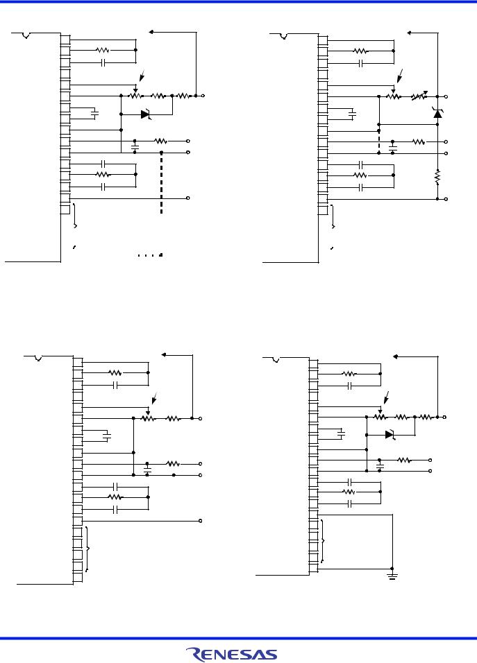
IN LO is tied to supply COMMON establishing the correct common mode voltage. If COMMON is not shorted to GND, the input voltage may float with respect to the power supply and COMMON acts as a pre-regulator for the reference. If COMMON is shorted to GND, the input is single ended (referred to supply GND) and the preregulator is overridden.
FIGURE 13. ICL7107 WITH AN EXTERNAL BAND-GAP REFERENCE (1.2V TYPE)
Since low TC zeners have breakdown voltages ~ 6.8V, diode must be placed across the total supply (10V). As in the case of Figure 12, IN LO may be tied to either COMMON or GND.
FIGURE 14. ICL7107 WITH ZENER DIODE REFERENCE
OSC 1 |
40 |
TO PIN 1 |
|
|
OSC 1 |
40 |
TO PIN 1 |
|
|
100kΩ |
|
|
100kΩ |
|
|
||||
OSC 2 |
39 |
|
|
OSC 2 |
39 |
|
|
||
|
|
|
|
|
|
||||
OSC 3 |
38 |
100pF |
SET VREF |
|
OSC 3 |
38 |
100pF |
SET VREF |
|
|
|
|
|
|
|||||
TEST |
37 |
= 1V |
|
TEST |
37 |
= 100mV |
|
||
|
|
|
|
||||||
REF HI |
36 |
|
|
|
REF HI |
36 |
|
|
|
REF LO |
35 |
|
|
V+ |
REF LO |
35 |
1kΩ |
10kΩ |
+5V |
CREF |
34 |
25kΩ |
24kΩ |
|
CREF |
34 |
15kΩ |
||
|
0.1µF |
|
|
||||||
CREF |
33 |
0.1µF |
|
|
CREF |
33 |
1.2V (ICL8069) |
||
|
|
|
|
||||||
COMMON |
32 |
|
1MΩ |
+ |
COMMON 32 |
|
1MΩ |
+ |
|
|
IN HI |
31 |
|
|
|||||
IN HI |
31 |
|
|
|
|
0.01µF |
IN |
||
0.01µF |
IN |
IN LO |
30 |
|
|||||
IN LO |
30 |
0.47µF |
|
- |
|||||
0.047µF |
|
- |
A-Z |
29 |
|
||||
A-Z |
29 |
|
47kΩ |
|
|
||||
470kΩ |
|
|
BUFF |
28 |
|
|
|||
BUFF |
28 |
|
|
|
|
|
|||
|
|
|
INT |
27 |
|
|
|
||
INT |
27 |
|
|
|
0.22µF |
|
|
||
0.22µF |
|
|
V - |
26 |
|
|
|||
V - |
26 |
|
V- |
|
|
|
|||
|
G2 |
25 |
|
|
|
||||
|
|
|
|
|
|||||
G2 |
25 |
|
|
|
|
|
|
||
|
|
|
C3 |
24 |
|
|
|
||
C3 |
24 |
|
|
|
TO DISPLAY |
|
|
||
TO DISPLAY |
|
|
A3 |
23 |
|
|
|||
A3 |
23 |
|
|
|
|
|
|||
|
|
G3 |
22 |
|
|
|
|||
|
|
|
|
|
|
||||
G3 |
22 |
|
|
|
|
|
|
||
|
|
|
GND |
21 |
|
|
|
||
BP/GND |
21 |
|
|
|
|
|
|
|
|
An external reference must be used in this application, since the voltage between V+ and V- is insufficient for correct operation of the internal reference.
FIGURE 15. ICL7106 AND ICL7107: RECOMMENDED COMPONENT |
FIGURE 16. ICL7107 OPERATED FROM SINGLE +5V |
VALUES FOR 2V FULL SCALE |
|
FN3082 |
Rev 9.00 |
|
Page 12 of 17 |
October 24, 2014 |
|
|
|
|
|
||
|
|
||
ICL7106, ICL7107, ICL7107S |
|
|
|
|
|
|
|
||
Typical Applications (Continued) |
|
|
|
|
|
|
|||
OSC 1 |
40 |
TO PIN 1 |
V+ |
OSC 1 |
40 |
|
TO PIN 1 |
|
|
100kΩ |
|
|
100kΩ |
|
|
||||
OSC 2 |
39 |
|
OSC 2 |
39 |
|
|
|
||
|
|
|
|
|
|
||||
OSC 3 |
38 |
100pF |
|
OSC 3 |
38 |
|
100pF |
SCALE |
|
TEST |
37 |
|
TEST |
37 |
|
|
|||
|
|
FACTOR |
|
||||||
REF HI |
36 |
|
|
REF HI |
36 |
|
|
ADJUST |
|
|
|
|
|
|
|
||||
REF LO |
35 |
|
|
REF LO |
35 |
|
100kΩ 1MΩ |
22kΩ |
|
CREF |
34 |
|
|
CREF |
34 |
|
|||
0.1µF |
|
0.1µF |
|
||||||
|
100kΩ220kΩ |
|
|||||||
CREF |
33 |
|
CREF |
33 |
|
||||
COMMON 32 |
|
|
COMMON |
32 |
|
|
|
|
|
IN HI |
31 |
|
IN HI |
31 |
0.01µF |
ZERO |
SILICON NPN |
IN LO |
30 |
|
IN LO |
30 |
ADJUST |
MPS 3704 OR |
|
0.47µF |
0.47µF |
|
SIMILAR |
||||
A-Z |
29 |
A-Z |
29 |
|
|||
47kΩ |
47kΩ |
|
|
||||
BUFF |
28 |
BUFF |
28 |
|
9V |
||
|
|
|
|||||
INT |
27 |
0.22µF |
INT |
27 |
0.22µF |
|
|
V - |
26 |
V - |
26 |
|
|
||
|
|
|
|
||||
G2 |
25 |
|
G2 |
25 |
|
|
|
C3 |
24 |
|
TO DISPLAY |
C3 |
24 |
|
TO DISPLAY |
|
A3 |
|
|
A3 |
|
|
|||
23 |
|
23 |
|
|||||
G3 |
|
|
|
G3 |
|
|
|
|
22 |
|
|
22 |
|
|
|
||
GND |
|
|
|
BP |
|
|
|
TO BACKPLANE |
21 |
|
|
21 |
|
|
|||
|
|
|
|
|||||
|
|
|
|
|
|
|
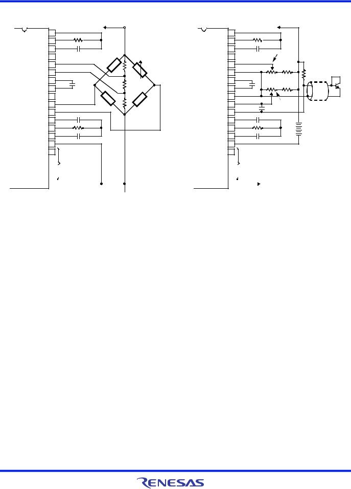
A silicon diode-connected transistor has a temperature coefficient of |
|
|
|
|
|
|
|
|
||
|
|
|
|
|
|
|
||
|
|
|
|
|
|
|
||
The resistor values within the bridge are determined by the desired |
about -2mV/°C. Calibration is achieved by placing the sensing |
|||||||
transistor in ice water and adjusting the zeroing potentiometer for a |
||||||||
sensitivity. |
||||||||
000.0 reading. The sensor should then be placed in boiling water and |
||||||||
|
|
|
|
|
|
|
||
|
|
|
|
|
|
|
the scale-factor potentiometer adjusted for a 100.0 reading. |
|
FIGURE 17. ICL7107 MEASURING RATIOMETRIC VALUES OF QUAD |
FIGURE 18. ICL7106 USED AS A DIGITAL CENTIGRADE |
|||||||
LOAD CELL |
THERMOMETER |
|||||||
FN3082 |
Rev 9.00 |
|
Page 13 of 17 |
October 24, 2014 |
|
|
|
|
|
||
|
|
||
ICL7106, ICL7107, ICL7107S |
|
|
|
|
|
|
|
|
|
|
|||
Typical Applications (Continued) |
|
|
|
|
|
|
|
|
|
||||
|
V+ |
|
|
|
|
|
|
|
+5V |
|
|
|
|
|
|
1 |
V+ |
OSC 1 |
40 |
|
|
|
1 |
V+ |
OSC 1 |
40 |
|
|
TO LOGIC |
2 |
D1 |
OSC 2 |
39 |
|
|
|
2 |
D1 |
OSC 2 |
39 |
|
|
3 |
C1 |
OSC 3 |
38 |
|
|
|
3 |
C1 |
OSC 3 |
38 |
|
|
|
VCC |
|
|
|
|
||||||||
|
4 |
B1 |
TEST |
37 |
|
|
|
4 |
B1 |
TEST |
37 |
|
|
|
|
|
|
|
|
||||||||
|
|
5 |
A1 |
REF HI |
36 |
|
|
|
5 |
A1 |
REF HI |
36 |
|
|
|
6 |
F1 |
REF LO |
35 |
TO |
|
TO LOGIC |
6 |
F1 |
REF LO |
35 |
|
|
|
7 |
G1 |
CREF |
34 |
LOGIC |
|
7 |
G1 |
CREF |
34 |
|
|
|
|
|
VCC |
|
|||||||||
|
|
GND |
|
|
|||||||||
|
|
8 |
E1 |
CREF |
33 |
|
|
|
8 |
E1 |
CREF |
33 |
|
|
|
9 |
D2 |
COMMON |
32 |
|
|
12kΩ |
9 |
D2 |
COMMON |
32 |
|
|
|
10 |
C2 |
IN HI |
31 |
|
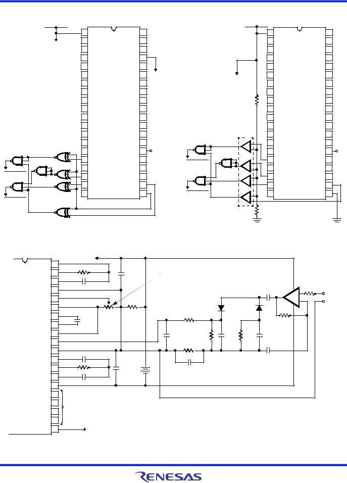
The LM339 is required to |
10 |
C2 |
IN HI |
31 |
|
|
|
|
11 |
B2 |
IN LO |
30 |
|
ensure logic compatibility |
11 |
B2 |
IN LO |
30 |
|
|
|
|
12 |
A2 |
A-Z |
29 |
|
with heavy display loading. |
12 |
A2 |
A-Z |
29 |
|
|
|
|
|
|
|
|
||||||||
|
|
13 |
F2 |
BUFF |
28 |
|
|
LM339 |
13 |
F2 |
BUFF |
28 |
|
|
|
14 |
E2 |
INT |
27 |
|
|
+- |
14 |
E2 |
INT |
27 |
|
|
|
15 |
D3 |
V- |
26 |
V- |
|
15 |
D3 |
V- |
26 |
V- |
|
|
|
|
|
||||||||||
|
|
16 |
B3 |
G2 |
25 |
|
O/RANGE |
+- |
16 |
B3 |
G2 |
25 |
|
|
|
17 |
F3 |
C3 |
24 |
|
17 |
F3 |
C3 |
24 |
|
||
O/RANGE |
|
|
|
|
|||||||||
|
18 |
E3 |
A3 |
23 |
|
|
+- |
18 |
E3 |
A3 |
23 |
|
|
|
|
19 |
AB4 |
G3 |
22 |
|
|
19 |
AB4 |
G3 |
22 |
|
|
|
|
|
|
|
|
||||||||
|
|
20 |
POL |
BP |
21 |
|
U/RANGE |
+- |
20 |
POL |
BP |
21 |
|
U/RANGE |
|
|
|
|
|
|
CD4023 OR |
|
|
|
|
|
|
|
|
|
|
|
|
|
74C10 |
|
33kΩ |
|
|
|
|
CD4023 OR |
|
|
|
|
|
|
|
|
|
|
|
|
|
CD4077 |
|
|
|
|
|
|
|
|
|
|
|
|
|
74C10 |
|
|
|
|
|
|
|
|
|
|
|
|
|
FIGURE 19. CIRCUIT FOR DEVELOPING UNDERRANGE AND OVERRANGE SIGNAL FROM ICL7106 OUTPUTS
FIGURE 20. CIRCUIT FOR DEVELOPING UNDERRANGE AND OVERRANGE SIGNALS FROM ICL7107 OUTPUT
OSC 1 |
40 |
TO PIN 1 |
|
|
|
|
|
|
|
|
|
|
100kΩ |
|
|
|
|
|
|
|
|
|
|
||
OSC 2 |
39 |
10µF |
|
|
|
|
|
|
|
|
|
|
|
|
SCALE FACTOR ADJUST |
|
|
|
|
|
|
||||
OSC 3 |
38 |
100pF |
|
|
(VREF = 100mV FOR AC TO RMS) |
|
|
CA3140 |
|
100kΩ |
||
TEST |
37 |
|
|
|
|
|
|
5µF |
+ |
|||
|
|
|
|
|
|
|
|
|
||||
REF HI |
36 |
|
|
|
|
|
|
|
|
|
AC IN |
|
|
|
|
|
|
|
|
|
|
- |
|||
|
|
|
|
|
|
|
|
|
|
|||
REF LO |
35 |
1kΩ |
22kΩ |
|
|
|
1N914 |
|
|
|
|
|
CREF |
34 |
|
|
470kΩ |
|
|
|
|
|
|
||
0.1µF |
|
|
|
|
|
|
2.2MΩ |
|
|
|||
CREF |
33 |
|
|
|
|
|
|
|
|
|
||
|
|
|
|
|
|
|
|
|
|
|
||
COMMON |
32 |
|
|
|
1µF |
10kΩ |
1µF |
10kΩ |
1µF |
|
|
|
IN HI |
31 |
|
|
|
|
|
|
|||||
|
|
|
|
4.3kΩ |
|
|
|
|
|
|
||
IN LO |
30 |
|
|
|
|
|
|
|
|
|
|
|
0.47µF |
|
|
|
|
|
|
0.22µF |
|
|
|||
A-Z |
29 |
|
|
|
|
|
|
|
|
|||
|
|
+ |
|
|
|
|
|
|
||||
47kΩ |
|
|
|
|
|
|
|
|
|
|||
BUFF |
28 |
10µF |
|
|
|
|
|
|
|
|
||
|
9V |
|
100pF |
|
|
|
|
|
|
|||
INT |
27 |
0.22µF |
|
- |
(FOR OPTIMUM BANDWIDTH) |
|
|
|
|
|
||
V - |
26 |
|
|
|
|
|
|
|
|
|
|
|
|
|
|
|
|
|
|
|
|
|
|
||
G2 |
25 |
|
|
|
|
|
|
|
|
|
|
|
C3 |
24 |
TO DISPLAY |
|
|
|
|
|
|
|
|
|
|
A3 |
23 |
|
|
|
|
|
|
|
|
|
|
|
|
|
|
|
|
|
|
|
|
|
|
||
G3 |
22 |
|
|
|
|
|
|
|
|
|
|
|
BP |
21 |
TO BACKPLANE |
|
|
|
|
|
|
|
|
|
|
Test is used as a common-mode reference level to ensure compatibility with most op amps.
FIGURE 21. AC TO DC CONVERTER WITH ICL7106
FN3082 |
Rev 9.00 |
|
Page 14 of 17 |
October 24, 2014 |
|
|
|
|
|
||
|
|
||
ICL7106, ICL7107, ICL7107S |
|
Typical Applications (Continued) |
|
+5V |
|
DM7407 |
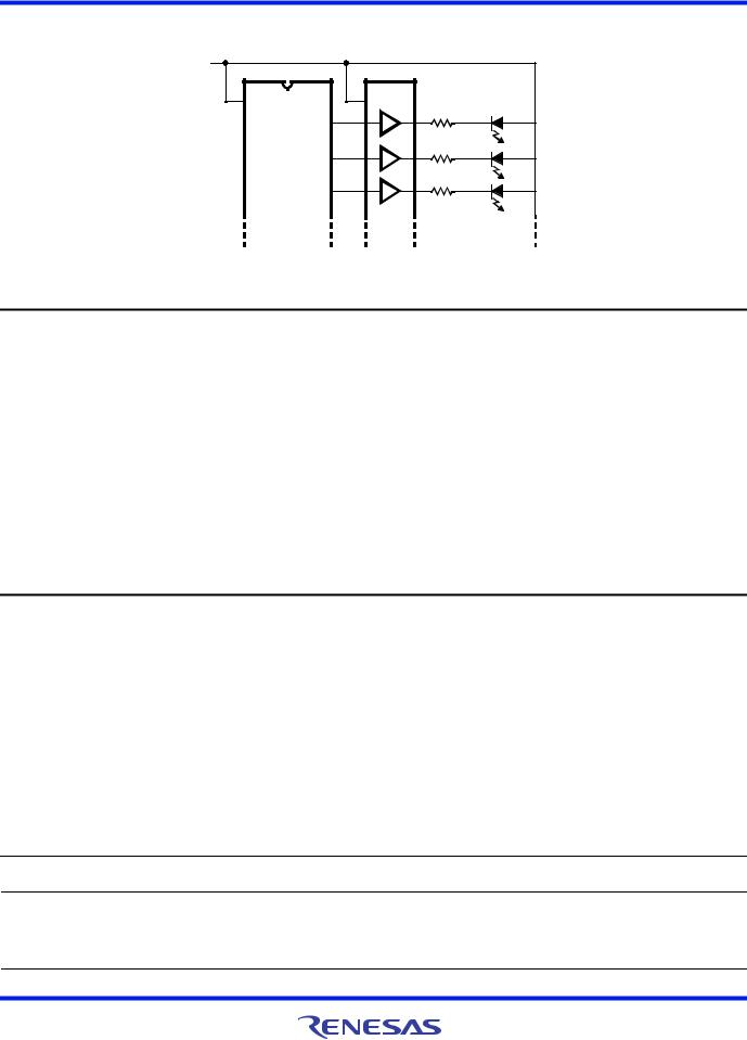
LED |
|
SEGMENTS |
ICL7107 |
130Ω |
|
130Ω |
|
130Ω |
FIGURE 22. DISPLAY BUFFERING FOR INCREASED DRIVE CURRENT
Revision History
The revision history provided is for informational purposes only and is believed to be accurate, but not warranted. Please go to the web to make sure that you have the latest revision.
DATE |
REVISION |
CHANGE |
|
|
|
October 24, 2014 |
FN3082.9 |
Updated to the newest template. |
|
|
Page 1: |
|
|
Updated copyright area. |
|
|
Ordering Information table - removed all non Pb-free parts (all obsolete: ICL7106CPL, ICL7106CM44, ICL7107CPL, |
|
|
ICL7107RCPL, ICL7107RCPLZ, ICL7107SCPL, ICL7107CM44, ICL7107CM44T) and removed ICL7107RCPLZ (obsolete). |
|
|
Page 2, Removed the PDIP pinout for the ICL7107R, as it is obsolete. |
|
|
Page 4, Reworded Electrical Spec Note 9 (formerly note 5) from: "Not tested, guaranteed by design." to: "Limit is not |
|
|
production tested. The maximum was established via characterization and/or design simulations." |
|
|
Page 15, Added Revision History and About Intersil verbiage. |
|
|
|
About Intersil
Intersil Corporation is a leading provider of innovative power management and precision analog solutions. The company's products address some of the largest markets within the industrial and infrastructure, mobile computing and high-end consumer markets.
For the most updated datasheet, application notes, related documentation and related parts, please see the respective product information page found at www.intersil.com.
You may report errors or suggestions for improving this datasheet by visiting www.intersil.com/ask. Reliability reports are also available from our website at www.intersil.com/support
© Copyright Intersil Americas LLC 2002-2014. All Rights Reserved.
All trademarks and registered trademarks are the property of their respective owners.
For additional products, see www.intersil.com/en/products.html
Intersil products are manufactured, assembled and tested utilizing ISO9001 quality systems as noted in the quality certifications found at www.intersil.com/en/support/qualandreliability.html
Intersil products are sold by description only. Intersil may modify the circuit design and/or specifications of products at any time without notice, provided that such modification does not, in Intersil's sole judgment, affect the form, fit or function of the product. Accordingly, the reader is cautioned to verify that datasheets are current before placing orders. Information furnished by Intersil is believed to be accurate and reliable. However, no responsibility is assumed by Intersil or its subsidiaries for its use; nor for any infringements of patents or other rights of third parties which may result from its use. No license is granted by implication or otherwise under any patent or patent rights of Intersil or its subsidiaries.
For information regarding Intersil Corporation and its products, see www.intersil.com
FN3082 |
Rev 9.00 |
|
Page 15 of 17 |
October 24, 2014 |
|
|
|
|
|
||
|
|
||
ICL7106, ICL7107, ICL7107S
Dual-In-Line Plastic Packages (PDIP)
|
|
|
|
|
|
|
|
|
|
|
|
|
|
|
|
|
|
|
|
|
|
|
|
|
|
|
|
|
|
|
|
|
|
|
|
|
|
|
|
|
|
|
|
|
|
|
|
|
|
|
|
|
|
|
|
|
|
|
|
|
|
|
|
|
|
|
|
|
|
|
|
|
N |
|
|
|
|
|
|
|
|
|
|
|
|
|
|
|
|
|
|
|
|
|
|
|
|
|
|
|
|
|
|
|
|
|
|
|
|
|
|||||||||||||
INDEX |
|
|
|
|
|
|
|
|
|
|
|
|
|
|
|
|
|
|
|
|
|
|
|
|
|
|
E1 |
|
|
|
|
|
|
|
|
|
|
|
|
|
|
|
|
|
|
|
|
|
|
|
|
||||||||||
|
1 2 3 |
|
|
|
|
|
|
|
|
|
|
|
N/2 |
|
|
|
|
|
|
|
|
|
|
|
|
|
|
|
|
|
|
|
|
|
|
|
|
|
|
|
|
|
|
||||||||||||||||||
|
|
|
|
|
|
|
|
|
|
|
|
|
|
|
|
|
|
|
|
|
|
|
|
|
|
|
|
|
|
|
|
|
|
|
|
|
|
|
|
|
|
||||||||||||||||||||
AREA |
|
|
|
|
|
|
|
|
|
|
|
|
|
|
|
|
|
|
|
|
|
|
|
|
|
|
|
|
|
|
|
|
|
|
|
|
|
|
|
|
|
|
|||||||||||||||||||
|
|
|
|
|
|
|
|
|
|
|
|
|
|
|
|
|
|
|
|
|
|
|
|
|
|
|
|
|
|
|
|
|
|
|
|
|
|
|
|
|
|
|
|
|
|
|
|
|
|
|
|
|
|
|
|
|
|
|
|
|
|
|
|
|
|
|
|
|
|
|
|
|
|
|
|
|
|
|
|
|
|
|
|
|
|
|
|
|
|
|
|
|
|
|
|
-B- |
|
|
|
|
|
|
|
|
|
|
|
|
|
|
|
|
|
|
|
|
|
|
|
|
|||
|
|
|
|
|
|
|
|
|
|
|
|
|
|
|
|
|
|
|
|
|
|
|
|
|
|
|
|
|
|
|
|
|
|
|
|
|
|
|
|
|
|
|
|
|
|
|
|
|
|
|
|
|
|
|
|
||||||
|
|
|
-A- |
|
|
|
|
|
|
|
|
|
|
|
D |
|
|
|
|
|
|
|
|
|
|
|
|
|
|
|
|
|
|
|
|
|
|
|
|
|
|
|
|
|
|
|
|
E |
|
|
|
|
|
||||||||
BASE |
|
|
|
|
|
|
|
|
|
|
|
|
|
|
|
|
|
|
|
|
|
|
|
|
|
|
|
|
|
|
|
|
|
|
|
|
|
|
|
|
|
|
|
|
|
|
|
|
|||||||||||||
|
|
|
|
|
|
|
|
|
|
|
|
|
|
|
|
|
|
|
|
|
|
|
|
|
|
|
|
|
|
|
|
|
|
|
|
|
|
|
|
|
|
|
|||||||||||||||||||
|
|
|
|
|
|
|
|
|
|
|
|
|
|
|
|
|
|
|
|
|
|
|
|
|
|
|
|
|
|
|
|
|
|
|
|
|
|
|
|
|
|
|
|
|
|
|
|
|
|
|
|
||||||||||
PLANE |
|
|
|
|
|
|
|
|
|
|
|
|
|
|
|
|
|
|
|
|
|
|
|
|
|
|
|
|
|
|
|
|
A2 |
|
A |
|
|
|
|
|
|
|
|
|
|
|
|||||||||||||||
SEATING |
|
|
|
|
|
|
|
|
|
|
|
|
|
|
|
|
|
|
|
|
|
|
|
|
|
|
|
|
-C- |
|
|
|
|
|
|
|
|
|
|
|
|
|
|
|
|
|
|
|
|
|
|
|
|
||||||||
PLANE |
|
|
|
|
|
|
|
|
|
|
|
|
|
|
|
|
|
|
|
|
|
|
|
|
|
|
|
|
|
|
|
|
|
|
|
|
|
|
|
L |
|
|
|
|
C |
||||||||||||||||
D1 |
|
|
|
|
|
|
|
|
|
|
|
|
|
|
|
|
|
|
|
|
|
|
|
|
|
|
|
|
|
|
|
|
|
|
|
|
|
|
|
|
|
|
|
|
|
|
|
|
|
|
|
|
L |
|
|||||||
|
|
|
|
|
|
|
|
|
|
|
|
|
|
|
|
|
|
|
|
|
|
|
|
|
|
|
|
|
|
A1 |
|
|
|
|
|
|
|
|
|
|
eA |
|
|
|
|||||||||||||||||
B1 |
|
|
|
|
|
|
|
|
|
|
|
|
|
|
|
|
|
|
|
|
|
|
|
e |
|
|
|
D1 |
|
|
|
|
|
|
|
|
|
|
eC |
|
|
|
|
|
|
|
|
|
|
|
|
|
|
|
|||||||
|
|
|
|
|
|
|
|
|
|
|
|
|
|
|
|
|
|
|
|
|
|
|
|
|
|
|
|
|
|
|
|
|
|
|
|
|
|
|
|
|
|
C |
|
|
|
|
|||||||||||||||
|
|
|
|
|
|
|
|
|
|
|
|
|
|
|
|
|
|
|
|
|
|
|
|
|
|
|
|
|
|
|
|
|
|
|
|
|
|
|
|
|
|
|
|
|
|
|
|
|
|||||||||||||
|
|
|
|
|
|
|
|
|
|
|
|
B |
|
|
|
|
|
|
|
|
|
|
|
|
|
|
|
|
|
|
|
|
|
|
|
|
|
|
|
|
|
|
|
|
|
|
|
|
|
|
|
|
|
|
|||||||
|
|
|
|
|
|
|
|
|
|
|
|
|
|
|
|
|
|
|
|
|
|
|
|
|
|
|
|
|
|
|
|
|
|
|
|
|
|
|
|
|
|
|
|
|
|
|
|
|
|
|
|
eB |
|
|
|
||||||
|
|
|
|
|
|
|
|
|
|
|
|
|
|
|
|
|
|
|
|
|
0.010 (0.25) |
|
|
|
C |
A |
B |
|
|
|
|
|
|
|
|
|
|
|
|
|
|
|
|
|
|
||||||||||||||||
|
|
|
|
|
|
|
|
|
|
|
|
|
|
|
|
|
|
|
|
|
|
|
|
|
|
|
|
|
|
|
|
|
|
|
|
|
|
|
|
|
|
||||||||||||||||||||
|
|
|
|
|
|
|
|
|
|
|
|
|
|
|
|
|
|
|
|
|
|
|
|
|
|
|
|
|
|
|
|
|
|
|
|
|
|
|
|
|
|
|
|
|
|
|
|
|
|
|
|
|
|
|
|
|
|
|
|
|
|
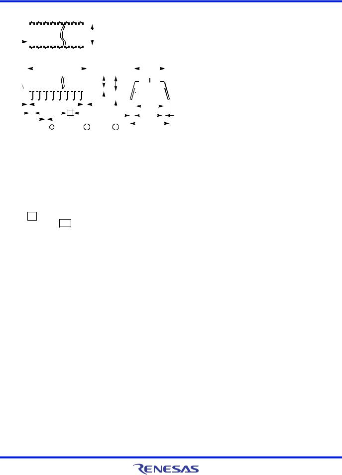
NOTES:
1.Controlling Dimensions: INCH. In case of conflict between English and Metric dimensions, the inch dimensions control.
2.Dimensioning and tolerancing per ANSI Y14.5M-1982.
3.Symbols are defined in the “MO Series Symbol List” in Section 2.2 of Publication No. 95.
4.Dimensions A, A1 and L are measured with the package seated in JEDEC seating plane gauge GS-3.
5.D, D1, and E1 dimensions do not include mold flash or protrusions. Mold flash or protrusions shall not exceed 0.010 inch (0.25mm).
6. E and eA are measured with the leads constrained to be perpendicular to datum -C- .
7.eB and eC are measured at the lead tips with the leads unconstrained. eC must be zero or greater.
8.B1 maximum dimensions do not include dambar protrusions. Dambar protrusions shall not exceed 0.010 inch (0.25mm).
9.N is the maximum number of terminal positions.
10.Corner leads (1, N, N/2 and N/2 + 1) for E8.3, E16.3, E18.3, E28.3, E42.6 will have a B1 dimension of 0.030 - 0.045 inch (0.76 - 1.14mm).
E40.6 (JEDEC MS-011-AC ISSUE B)
40 LEAD DUAL-IN-LINE PLASTIC PACKAGE
|
INCHES |
MILLIMETERS |
|
||||
SYMBOL |
|
|
|
|
|
|
NOTES |
MIN |
|
MAX |
MIN |
|
MAX |
||
|
|
|
|
|
|
|
|
A |
- |
|
0.250 |
- |
|
6.35 |
4 |
|
|
|
|
|
|
|
|
A1 |
0.015 |
|
- |
0.39 |
|
- |
4 |
|
|
|
|
|
|
|
|
A2 |
0.125 |
|
0.195 |
3.18 |
|
4.95 |
- |
|
|
|
|
|
|
|
|
B |
0.014 |
|
0.022 |
0.356 |
|
0.558 |
- |
|
|
|
|
|
|
|
|
B1 |
0.030 |
|
0.070 |
0.77 |
|
1.77 |
8 |
|
|
|
|
|
|
|
|
C |
0.008 |
|
0.015 |
0.204 |
|
0.381 |
- |
|
|
|
|
|
|
|
|
D |
1.980 |
|
2.095 |
50.3 |
|
53.2 |
5 |
|
|
|
|
|
|
|
|
D1 |
0.005 |
|
- |
0.13 |
|
- |
5 |
|
|
|
|
|
|
|
|
E |
0.600 |
|
0.625 |
15.24 |
|
15.87 |
6 |
|
|
|
|
|
|
|
|
E1 |
0.485 |
|
0.580 |
12.32 |
|
14.73 |
5 |
|
|
|
|
|
|
||
e |
0.100 BSC |
2.54 BSC |
- |
||||
|
|
|
|
||||
eA |
0.600 BSC |
15.24 BSC |
6 |
||||
eB |
- |
|
0.700 |
- |
|
17.78 |
7 |
L |
0.115 |
|
0.200 |
2.93 |
|
5.08 |
4 |
|
|
|
|
|
|
|
|
N |
|
40 |
|
40 |
9 |
||
|
|
|
|
|
|
|
|
Rev. 0 12/93
FN3082 |
Rev 9.00 |
|
Page 16 of 17 |
October 24, 2014 |
|
|
|
|
|
||
|
|
||
ICL7106, ICL7107, ICL7107S
Metric Plastic Quad Flatpack Packages (MQFP)
D |
|
|
|
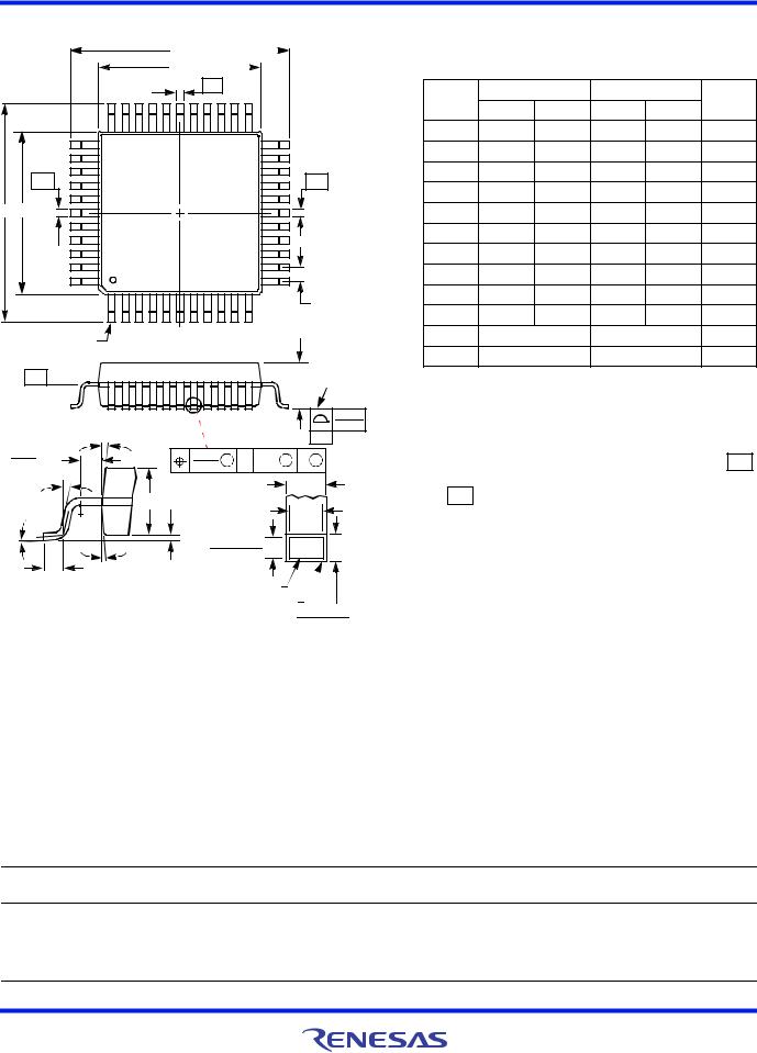
Q44.10x10 (JEDEC MS-022AB ISSUE B) |
|
|
|
||
D1 |
|
|
|
44 LEAD METRIC PLASTIC QUAD FLATPACK PACKAGE |
|
|
|
|
|
-D- |
|
|
INCHES |
MILLIMETERS |
|
||
|
|
|
|
SYMBOL |
MIN |
MAX |
MIN |
MAX |
NOTES |
|
|
|
|
A |
- |
0.096 |
- |
2.45 |
- |
|
|
|
|
A1 |
0.004 |
0.010 |
0.10 |
0.25 |
- |
|
-A- |
|
-B- |
A2 |
0.077 |
0.083 |
1.95 |
2.10 |
- |
|
|
b |
0.012 |
0.018 |
0.30 |
0.45 |
6 |
||
|
|
|
|
||||||
E |
E1 |
|
|
b1 |
0.012 |
0.016 |
0.30 |
0.40 |
- |
|
|
|
|
D |
0.515 |
0.524 |
13.08 |
13.32 |
3 |
|
|
|
|
D1 |
0.389 |
0.399 |
9.88 |
10.12 |
4, 5 |
|
|
|
|
E |
0.516 |
0.523 |
13.10 |
13.30 |
3 |
|
|
|
e |
E1 |
0.390 |
0.398 |
9.90 |
10.10 |
4, 5 |
|
|
|
L |
0.029 |
0.040 |
0.73 |
1.03 |
- |
|
|
|
|
|
||||||
|
|
PIN 1 |
|
N |
|
44 |
|
44 |
7 |
|
|
|
|
|
|
|
|
|
|
|
|
|
|
e |
0.032 BSC |
0.80 BSC |
- |
||
|
-H- |
|
SEATING |
|
|
|
|
|
Rev. 2 4/99 |
|
A |
PLANE |
|
|
|
|
|
||
|
NOTES: |
|
|
|
|
|
|||
|
|
|
|
|
|
|
|
|
|
|
|
|
|
0.076 |
|
|
|
|
0.003 |
0.40 |
|
12o-16o |
|
-C- |
MIN |
|
0.20 |
D S |
|
0.016 |
|
0.008 M C A-B S |
||
0o MIN |
|
|
b |
|
|
|
A2 |
|
|
0o-7o |
|
A1 |
b1 |
|
|
|
|
||
|
|
|
0.13/0.17 |
|
|
L |
12o-16o |
0.005/0.007 |
|
|
|
|
||
|
|
|
|
|
|
|
|
BASE METAL |
|
|
|
|
WITH PLATING |
0.13/0.23 |
|
|
|
|
0.005/0.009 |
1.Controlling dimension: MILLIMETER. Converted inch dimensions are not necessarily exact.
2.All dimensions and tolerances per ANSI Y14.5M-1982.
3. Dimensions D and E to be determined at seating plane -C- .
4.Dimensions D1 and E1 to be determined at datum plane -H- .
5.Dimensions D1 and E1 do not include mold protrusion. Allowable protrusion is 0.25mm (0.010 inch) per side.
6.Dimension b does not include dambar protrusion. Allowable dambar protrusion shall be 0.08mm (0.003 inch) total.
7.“N” is the number of terminal positions.
© Copyright Intersil Americas LLC 2002-2014. All Rights Reserved.
All trademarks and registered trademarks are the property of their respective owners.
For additional products, see www.intersil.com/en/products.html
Intersil products are manufactured, assembled and tested utilizing ISO9001 quality systems as noted in the quality certifications found at www.intersil.com/en/support/qualandreliability.html
Intersil products are sold by description only. Intersil may modify the circuit design and/or specifications of products at any time without notice, provided that such modification does not, in Intersil's sole judgment, affect the form, fit or function of the product. Accordingly, the reader is cautioned to verify that datasheets are current before placing orders. Information furnished by Intersil is believed to be accurate and reliable. However, no responsibility is assumed by Intersil or its subsidiaries for its use; nor for any infringements of patents or other rights of third parties which may result from its use. No license is granted by implication or otherwise under any patent or patent rights of Intersil or its subsidiaries.
For information regarding Intersil Corporation and its products, see www.intersil.com
FN3082 |
Rev 9.00 |
|
Page 17 of 17 |
October 24, 2014 |
|
|
|
|
|
||
|
|
||

Mouser Electronics
Authorized Distributor
Click to View Pricing, Inventory, Delivery & Lifecycle Information:
Renesas Electronics:
ICL7106CM44Z ICL7106CM44ZT ICL7106CPLZ ICL7107CM44Z ICL7107CM44ZT ICL7107CPLZ
