

Материалы к лабораторным работам / Даташиты / sn74hc161
.pdfSN54HC161, SN74HC161 4 BIT SYNCHRONOUS BINARY COUNTERS
|
|
SCLS297D − JANUARY 1996 − REVISED SEPTEMBER 2003 |
|
|
|
D Wide Operating Voltage Range of 2 V to 6 V |
D Low Input Current of 1 A Max |
|
D Outputs Can Drive Up To 10 LSTTL Loads |
D Internal Look-Ahead for Fast Counting |
|
D Low Power Consumption, 80- A Max ICC |
D Carry Output for n-Bit Cascading |
|
D Typical tpd = 14 ns |
D |
Synchronous Counting |
D ±4-mA Output Drive at 5 V |
D |
Synchronously Programmable |
SN54HC161 . . . J OR W PACKAGE |
|
SN54HC161 . . . FK PACKAGE |
SN74HC161 . . . D, N, NS, OR PW PACKAGE |
|
(TOP VIEW) |
|
(TOP VIEW) |
|
|
CLK |
CLR |
NC |
V |
RCO |
|
|
|
|
|
|
|
|
|
|
CC |
|
|
CLR |
1 |
16 |
VCC |
|
|
|
|
|
|
|
CLK |
2 |
15 |
RCO |
A |
3 |
2 |
1 |
20 19 |
QA |
|
A |
3 |
14 |
QA |
4 |
|
|
|
18 |
||
B |
4 |
13 |
QB |
B |
5 |
|
|
|
17 |
QB |
C |
5 |
12 |
QC |
NC |
6 |
|
|
|
16 |
NC |
C |
7 |
|
|
|
15 |
QC |
||||
D |
6 |
11 |
QD |
|
|
|
||||
|
|
|
14 |
|||||||
ENP |
7 |
10 |
ENT |
D |
8 |
|
|
|
QD |
|
GND |
8 |
9 |
LOAD |
|
9 |
10 11 12 13 |
|
|||
|
ENP |
GND |
NC |
LOAD |
ENT |
|
||||
|
|
|
|
|
|
|||||
|
|
|
|
NC − No internal connection |
|
|||||
description/ordering information
These synchronous, presettable counters feature an internal carry look-ahead for application in high-speed counting designs. The ’HC161 devices are 4-bit binary counters. Synchronous operation is provided by having all flip-flops clocked simultaneously so that the outputs change coincident with each other when so instructed by the count-enable (ENP, ENT) inputs and internal gating. This mode of operation eliminates the output counting spikes that are normally associated with synchronous (ripple-clock) counters. A buffered clock (CLK) input triggers the four flip-flops on the rising (positive-going) edge of the clock waveform.
ORDERING INFORMATION
T |
PACKAGE† |
ORDERABLE |
TOP-SIDE |
||
|
|
||||
A |
|
|
PART NUMBER |
MARKING |
|
|
|
|
|||
|
PDIP − N |
Tube of 25 |
SN74HC161N |
SN74HC161N |
|
|
|
|
|
|
|
|
|
Tube of 40 |
SN74HC161D |
|
|
|
|
|
|
|
|
|
SOIC − D |
Reel of 2500 |
SN74HC161DR |
HC161 |
|
−40 °C to 85°C |
|
Reel of 250 |
SN74HC161DT |
|
|
|
|
|
|
||
SOP − NS |
Reel of 2000 |
SN74HC161NSR |
HC161 |
||
|
|||||
|
|
|
|
|
|
|
|
Tube of 90 |
SN74HC161PW |
|
|
|
|
|
|
|
|
|
TSSOP − PW |
Reel of 2000 |
SN74HC161PWR |
HC161 |
|
|
|
Reel of 250 |
SN74HC161PWT |
|
|
|
|
|
|
|
|
|
CDIP − J |
Tube of 25 |
SNJ54HC161J |
SNJ54HC161J |
|
−55 °C to 125°C |
|
|
|
|
|
CFP − W |
Tube of 150 |
SNJ54HC161W |
SNJ54HC161W |
||
|
|
|
|
|
|
|
LCCC − FK |
Tube of 55 |
SNJ54HC161FK |
SNJ54HC161FK |
|
|
|
|
|
|
|
†Package drawings, standard packing quantities, thermal data, symbolization, and PCB design guidelines are available at www.ti.com/sc/package.
Please be aware that an important notice concerning availability, standard warranty, and use in critical applications of Texas Instruments semiconductor products and disclaimers thereto appears at the end of this data sheet.
PRODUCTION DATA information is current as of publication date. Products conform to specifications per the terms of Texas Instruments standard warranty. Production processing does not necessarily include testing of all parameters.
Copyright 2003, Texas Instruments Incorporated
On products compliant to MIL PRF 38535, all parameters are tested unless otherwise noted. On all other products, production processing does not necessarily include testing of all parameters.
POST OFFICE BOX 655303 • DALLAS, TEXAS 75265 |
1 |
SN54HC161, SN74HC161
4 BIT SYNCHRONOUS BINARY COUNTERS
SCLS297D − JANUARY 1996 − REVISED SEPTEMBER 2003
description/ordering information (continued)
These counters are fully programmable; that is, they can be preset to any number between 0 and 9 or 15. As presetting is synchronous, setting up a low level at the load input disables the counter and causes the outputs to agree with the setup data after the next clock pulse, regardless of the levels of the enable inputs.
The clear function for the ’HC161 devices is asynchronous. A low level at the clear (CLR) input sets all four of the flip-flop outputs low, regardless of the levels of the CLK, load (LOAD), or enable inputs.
The carry look-ahead circuitry provides for cascading counters for n-bit synchronous applications without additional gating. Instrumental in accomplishing this function are ENP, ENT, and a ripple-carry output (RCO). Both ENP and ENT must be high to count, and ENT is fed forward to enable RCO. Enabling RCO produces a high-level pulse while the count is maximum (9 or 15 with QA high). This high-level overflow ripple-carry pulse can be used to enable successive cascaded stages. Transitions at ENP or ENT are allowed, regardless of the level of CLK.
These counters feature a fully independent clock circuit. Changes at control inputs (ENP, ENT, or LOAD) that modify the operating mode have no effect on the contents of the counter until clocking occurs. The function of the counter (whether enabled, disabled, loading, or counting) is dictated solely by the conditions meeting the stable setup and hold times.
2 |
POST OFFICE BOX 655303 • DALLAS, TEXAS 75265 |
|
|
|
|
SN54HC161, SN74HC161 |
|
|
|
4 BIT SYNCHRONOUS BINARY COUNTERS |
|
|
|
|
SCLS297D − JANUARY 1996 − REVISED SEPTEMBER 2003 |
|
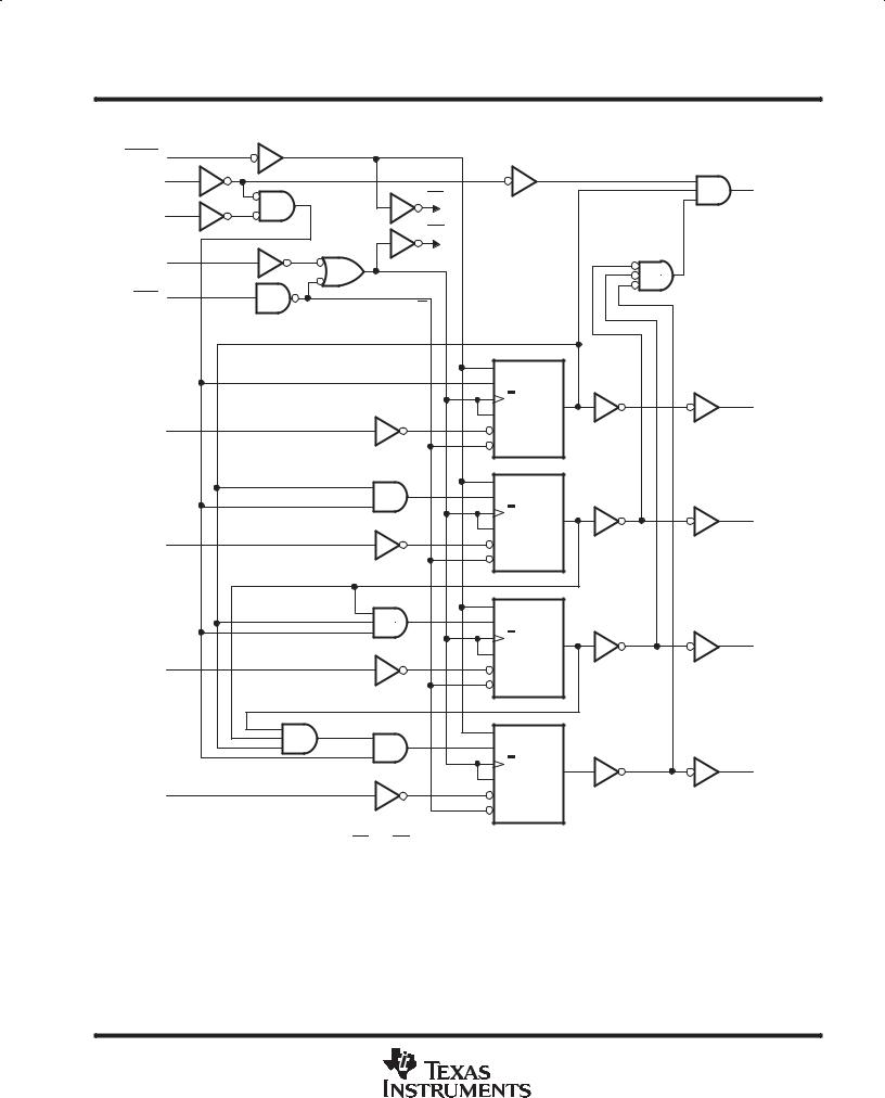
logic diagram (positive logic) |
|
|
|
|
LOAD |
9 |
|
|
|
|
|
|
|
|
ENT |
10 |
|
|
15 |
|
|
|
||
|
|
LD† |
|
RCO |
|
7 |
|
|
|
ENP |
|
|
|
|
|
|
|
|
|
|
|
CK† |
|
|
CLK |
2 |
|
|
|
|
|
|
|
|
|
1 |
CK |
LD |
|
CLR |
|
|
|
|
|
R |
|
|
|
|
|
|
|
|
|
|
|
M1 |
|
|
|
|
G2 |
|
|
|
|
1, 2T/1C3 |
14 |
|
3 |
|
G4 |
QA |
A |
|
3D |
|
|
|
|
|
||
|
|
|
4R |
|
|
|
|
M1 |
|
|
|
|
G2 |
|
|
|
|
1, 2T/1C3 |
13 |
|
4 |
|
G4 |
QB |
B |
|
3D |
|
|
|
|
|
||
|
|
|
4R |
|
|
|
|
M1 |
|
|
|
|
G2 |
|
|
|
|
1, 2T/1C3 |
12 |
|
5 |
|
G4 |
QC |
C |
|
3D |
|
|
|
|
|
||
|
|
|
4R |
|
|
|
|
M1 |
|
|
|
|
G2 |
|
|
|
|
1, 2T/1C3 |
11 |
|
6 |
|
G4 |
QD |
D |
|
3D |
|
|
|
|
|
||
|
|
|
4R |
|
†For simplicity, routing of complementary signals LD and CK is not shown on this overall logic diagram. The uses of these signals are shown on the logic diagram of the D/T flip-flops.
Pin numbers shown are for the D, J, N, NS, PW, and W packages.
POST OFFICE BOX 655303 • DALLAS, TEXAS 75265 |
3 |
SN54HC161, SN74HC161
4 BIT SYNCHRONOUS BINARY COUNTERS
SCLS297D − JANUARY 1996 − REVISED SEPTEMBER 2003
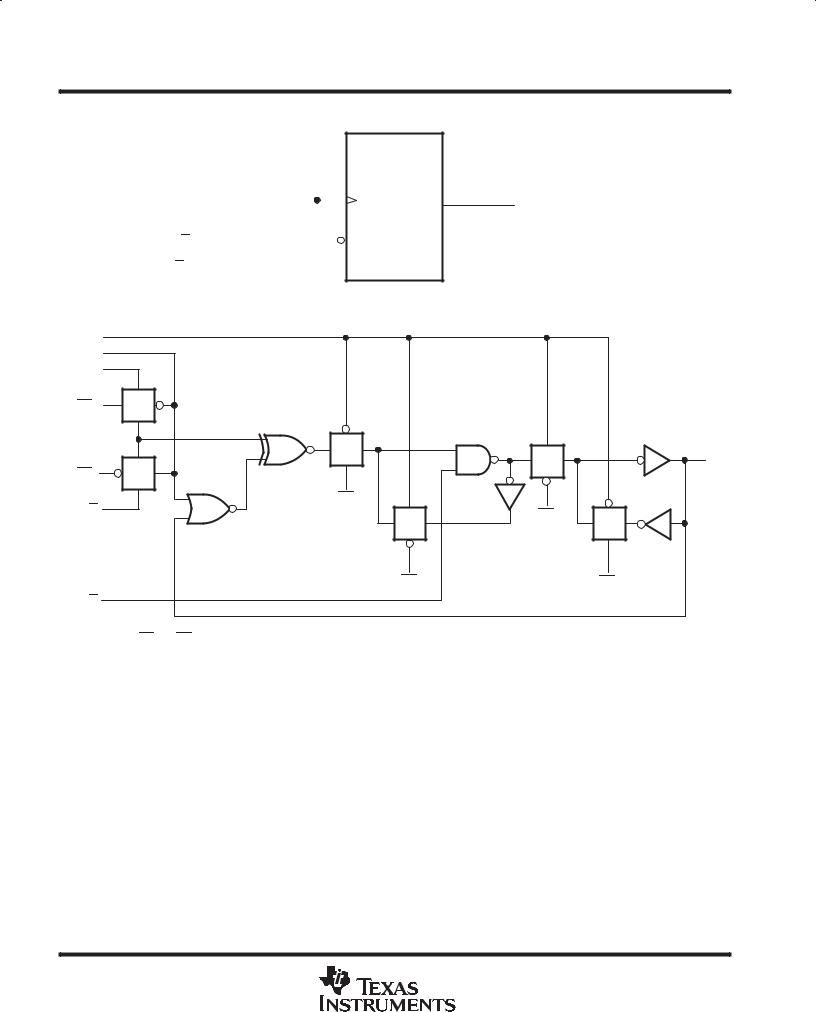
logic symbol, each D/T flip-flop
LD (Load) |
|
|
M1 |
|
||
|
|
|
||||
TE (Toggle Enable) |
|
|
G2 |
|
||
|
|
|
||||
CK (Clock) |
|
|
|
|
|
|
|
|
|
1, 2T/1C3 |
Q (Output) |
||
|
|
|||||
|
|
|
G4 |
|||
|
|
|
|
|||
|
|
|
|
|||
D (Inverted Data)  3D
3D
R (Inverted Reset)  4R
4R
logic diagram, each D/T flip-flop (positive logic)
CK |
|
LD |
|
TE |
|
LD† |
TG |
LD† |
TG |
D |
|
R
TG |
CK†
TG |
CK†
TG |
Q |
CK† |
TG |
|
|
|
CK† |
†The origins of LD and CK are shown in the logic diagram of the overall device.
4 |
POST OFFICE BOX 655303 • DALLAS, TEXAS 75265 |
SN54HC161, SN74HC161 4 BIT SYNCHRONOUS BINARY COUNTERS
SCLS297D − JANUARY 1996 − REVISED SEPTEMBER 2003
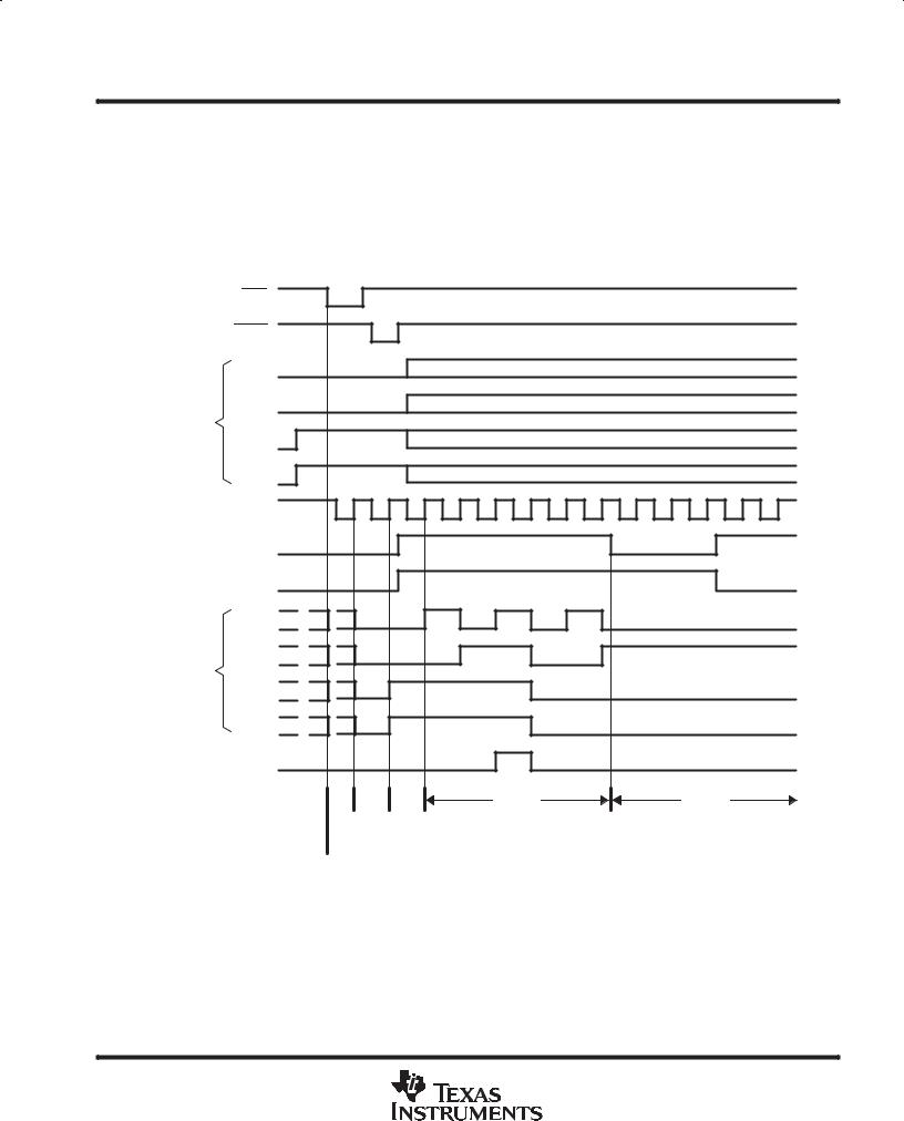
typical clear, preset, count, and inhibit sequence
The following sequence is illustrated below:
1.Clear outputs to zero (asynchronous)
2.Preset to binary 12
3.Count to 13, 14, 15, 0, 1, and 2
4.Inhibit
CLR
LOAD
A
B
Data
Inputs
C
D
CLK
ENP
ENT
QA
Data QB
Outputs
QC
QD
RCO
12 |
13 |
14 |
15 |
0 |
1 |
2 |
|
|
|
Count |
|
Inhibit |
|
Sync Preset |
|
|
|
|
|
|
Clear |
|
|
|
|
|
|
Async |
|
|
|
|
|
|
Clear |
|
|
|
|
|
|
POST OFFICE BOX 655303 • DALLAS, TEXAS 75265 |
5 |

SN54HC161, SN74HC161
4 BIT SYNCHRONOUS BINARY COUNTERS
SCLS297D − JANUARY 1996 − REVISED SEPTEMBER 2003
absolute maximum ratings over operating free-air temperature range (unless otherwise noted)†
Supply voltage range, VCC . . . . . . . . . . . . . . . . . . . . . . . . . . . . . . . . . . . . . . . . . . . . . . . . . . . . . . . . . |
. −0.5 V to 7 V |
Input clamp current, IIK (VI < 0 or VI > VCC) (see Note 1) . . . . . . . . . . . . . . . . . . . . . . . . . . . . . . |
. . . . . . ±20 mA |
Output clamp current, IOK (VO < 0 or VO > VCC) (see Note 1) . . . . . . . . . . . . . . . . . . . . . . . . . . |
. . . . . . ±20 mA |
Continuous output current, IO (VO = 0 to VCC) . . . . . . . . . . . . . . . . . . . . . . . . . . . . . . . . . . . . . . . . |
. . . . . . ±25 mA |
Continuous current through VCC or GND . . . . . . . . . . . . . . . . . . . . . . . . . . . . . . . . . . . . . . . . . . . . . |
. . . . . . ±50 mA |
Package thermal impedance, θJA (see Note 2): D package . . . . . . . . . . . . . . . . . . . . . . . . . . . . . |
. . . . . . 73°C/W |
N package . . . . . . . . . . . . . . . . . . . . . . . . . . . . . |
. . . . . . 67°C/W |
NS package . . . . . . . . . . . . . . . . . . . . . . . . . . . |
. . . . . . 64°C/W |
PW package . . . . . . . . . . . . . . . . . . . . . . . . . . . |
. . . . . 108°C/W |
Storage temperature range, Tstg . . . . . . . . . . . . . . . . . . . . . . . . . . . . . . . . . . . . . . . . . . . . . . . . . . . |
−65 °C to 150°C |
†Stresses beyond those listed under “absolute maximum ratings” may cause permanent damage to the device. These are stress ratings only, and functional operation of the device at these or any other conditions beyond those indicated under “recommended operating conditions” is not implied. Exposure to absolute-maximum-rated conditions for extended periods may affect device reliability.
NOTES: 1. The input and output voltage ratings may be exceeded if the input and output current ratings are observed. 2. The package thermal impedance is calculated in accordance with JESD 51-7.
recommended operating conditions (see Note 3)
|
|
|
|
|
|
SN54HC161 |
|
SN74HC161 |
|
UNIT |
||
|
|
|
|
|
|
|
|
|
|
|
|
|
|
|
|
|
|
|
MIN |
NOM |
MAX |
MIN |
NOM |
MAX |
|
|
|
|
|
|
|
|
||||||
|
|
|
|
|
|
|
|
|
|
|
|
|
VCC |
|
Supply voltage |
|
|
|
2 |
5 |
6 |
2 |
5 |
6 |
V |
|
|
|
VCC |
= 2 V |
1.5 |
|
|
1.5 |
|
|
|
|
VIH |
|
High-level input voltage |
VCC |
= 4.5 V |
3.15 |
|
|
3.15 |
|
|
V |
|
|
|
|
VCC |
= 6 V |
4.2 |
|
|
4.2 |
|
|
|
|
|
|
|
VCC |
= 2 V |
|
|
0.5 |
|
|
0.5 |
|
|
VIL |
|
Low-level input voltage |
VCC |
= 4.5 V |
|
|
1.35 |
|
|
1.35 |
V |
|
|
|
|
VCC |
= 6 V |
|
|
1.8 |
|
|
1.8 |
|
|
VI |
|
Input voltage |
|
|
|
0 |
|
VCC |
0 |
|
VCC |
V |
VO |
|
Output voltage |
|
|
|
0 |
|
VCC |
0 |
|
VCC |
V |
|
|
|
VCC |
= 2 V |
|
|
1000 |
|
|
1000 |
|
|
∆ ∆ |
‡ |
Input transition rise/fall time |
V |
CC |
= 4.5 V |
|
|
500 |
|
|
500 |
ns |
t/ v |
|
|
|
|
|
|
|
|
||||
|
|
|
VCC = 6 V |
|
|
400 |
|
|
400 |
|
||
TA |
|
Operating free-air temperature |
|
|
|
−55 |
|
125 |
−40 |
|
85 |
°C |
NOTE 3: All unused inputs of the device must be held at VCC or GND to ensure proper device operation. Refer to the TI application report,
Implications of Slow or Floating CMOS Inputs, literature number SCBA004.
‡If this device is used in the threshold region (from VILmax = 0.5 V to VIHmin = 1.5 V), there is a potential to go into the wrong state from induced grounding, causing double clocking. Operating with the inputs at tt = 1000 ns and VCC = 2 V does not damage the device; however, functionally, the CLK inputs are not ensured while in the shift, count, or toggle operating modes.
6 |
POST OFFICE BOX 655303 • DALLAS, TEXAS 75265 |

SN54HC161, SN74HC161 4 BIT SYNCHRONOUS BINARY COUNTERS
SCLS297D − JANUARY 1996 − REVISED SEPTEMBER 2003
electrical characteristics over recommended operating free-air temperature range (unless otherwise noted)
PARAMETER |
TEST CONDITIONS |
VCC |
|
TA = 25°C |
|
SN54HC161 |
SN74HC161 |
UNIT |
||
MIN |
TYP |
MAX |
MIN MAX |
MIN MAX |
||||||
|
|
|
|
|
||||||
|
|
|
|
|
|
|
|
|
|
|
|
|
|
2 V |
1.9 |
1.998 |
|
1.9 |
1.9 |
|
|
|
|
|
|
|
|
|
|
|
|
|
|
|
IOH = −20 µA |
4.5 V |
4.4 |
4.499 |
|
4.4 |
4.4 |
|
|
VOH |
VI = VIH or VIL |
|
6 V |
5.9 |
5.999 |
|
5.9 |
5.9 |
V |
|
|
|
IOH = −4 mA |
4.5 V |
3.98 |
4.3 |
|
3.7 |
3.84 |
|
|
|
|
IOH = −5.2 mA |
6 V |
5.48 |
5.8 |
|
5.2 |
5.34 |
|
|
|
|
|
2 V |
|
0.002 |
0.1 |
0.1 |
0.1 |
|
|
|
|
|
|
|
|
|
|
|
|
|
|
|
IOL = 20 µA |
4.5 V |
|
0.001 |
0.1 |
0.1 |
0.1 |
|
|
VOL |
VI = VIH or VIL |
|
6 V |
|
0.001 |
0.1 |
0.1 |
0.1 |
V |
|
|
|
IOL = 4 mA |
4.5 V |
|
0.17 |
0.26 |
0.4 |
0.33 |
|
|
|
|
IOL = 5.2 mA |
6 V |
|
0.15 |
0.26 |
0.4 |
0.33 |
|
|
II |
VI = VCC or 0 |
6 V |
|
±0.1 |
±100 |
±1000 |
±1000 |
nA |
||
ICC |
VI = VCC or 0, IO = 0 |
6 V |
|
|
8 |
160 |
80 |
µA |
||
Ci |
|
|
2 V to 6 V |
|
3 |
10 |
10 |
10 |
pF |
|
timing requirements over recommended operating free-air temperature range (unless otherwise noted)
|
|
|
|
|
|
VCC |
TA = 25°C |
SN54HC161 |
SN74HC161 |
UNIT |
|
|
|
|
|
|
|
MIN MAX |
MIN MAX |
MIN MAX |
|
||
|
|
|
|
|
|
|
|
|
|||
|
|
|
|
|
|
|
|
|
|
|
|
|
|
|
|
|
|
2 V |
6 |
4.2 |
5 |
|
|
|
|
|
|
|
|
|
|
|
|
|
|
fclock |
Clock frequency |
4.5 V |
31 |
21 |
25 |
MHz |
|
||||
|
|
|
|
|
|
6 V |
36 |
25 |
29 |
|
|
|
|
|
|
|
|
|
|
|
|
|
|
|
|
|
|
|
|
2 V |
80 |
120 |
100 |
|
|
|
|
|
|
|
|
|
|
|
|
|
|
|
|
CLK high or low |
4.5 V |
16 |
24 |
20 |
|
|
|||
tw |
Pulse duration |
|
|
|
|
6 V |
14 |
20 |
17 |
ns |
|
|
|
|
|
|
|
|
|
|
|||
|
|
|
|
2 V |
80 |
120 |
100 |
|
|||
|
|
|
|
|
|
|
|
||||
|
|
|
|
|
|
|
|
|
|
||
|
|
|
|
low |
4.5 V |
16 |
24 |
20 |
|
|
|
|
|
|
CLR |
|
|
||||||
|
|
|
|
|
|
6 V |
14 |
20 |
17 |
|
|
|
|
|
|
|
|
|
|
|
|
|
|
|
|
|
|
|
|
2 V |
150 |
225 |
190 |
|
|
|
|
|
|
|
|
|
|
|
|
||
|
|
A, B, C, or D |
4.5 V |
30 |
45 |
38 |
|
|
|||
|
|
|
|
|
|
6 V |
26 |
38 |
32 |
|
|
|
|
|
|
|
|
|
|
|
|
|
|
|
|
|
|
|
|
2 V |
135 |
205 |
170 |
|
|
|
|
|
|
|
|
|
|
|
|||
|
|
|
|
|
low |
4.5 V |
27 |
41 |
34 |
|
|
|
|
|
LOAD |
|
|
||||||
tsu |
Setup time before CLK↑ |
|
|
|
|
6 V |
23 |
35 |
29 |
ns |
|
|
|
|
|
|
|
|
|||||
|
|
|
|
2 V |
170 |
255 |
215 |
|
|||
|
|
|
|
|
|
|
|
||||
|
|
|
|
|
|
|
|
|
|||
|
|
ENP, ENT |
4.5 V |
34 |
51 |
43 |
|
|
|||
|
|
|
|
|
|
6 V |
29 |
43 |
37 |
|
|
|
|
|
|
|
|
|
|
|
|
|
|
|
|
|
|
|
|
2 V |
125 |
190 |
155 |
|
|
|
|
|
|
|
|
|
|
|
|||
|
|
|
|
inactive |
4.5 V |
25 |
38 |
31 |
|
|
|
|
|
|
CLR |
|
|
||||||
|
|
|
|
|
|
6 V |
21 |
32 |
26 |
|
|
|
|
|
|
|
|
|
|
|
|
|
|
|
|
|
|
|
|
2 V |
0 |
0 |
0 |
|
|
th |
Hold time, all synchronous inputs after CLK↑ |
|
|
|
|
ns |
|
||||
4.5 V |
0 |
0 |
0 |
|
|||||||
|
|
|
|
|
|
6 V |
0 |
0 |
0 |
|
|
|
|
|
|
|
|
|
|
|
|
|
|
|
|
|
|
|
|
|
|
|
|
|
|
|
|
|
|
|
|
|
|
|
|
|
|
POST OFFICE BOX 655303 • DALLAS, TEXAS 75265 |
7 |

SN54HC161, SN74HC161
4 BIT SYNCHRONOUS BINARY COUNTERS
SCLS297D − JANUARY 1996 − REVISED SEPTEMBER 2003
switching characteristics over recommended operating free-air temperature range, CL = 50 pF (unless otherwise noted) (see Figure 1)
PARAMETER |
FROM |
TO |
VCC |
|
TA = 25°C |
|
SN54HC161 |
SN74HC161 |
UNIT |
||
(INPUT) |
(OUTPUT) |
MIN |
TYP |
MAX |
MIN MAX |
MIN MAX |
|||||
|
|
|
|
|
2 V |
6 |
14 |
|
4.2 |
5 |
|
|
|
|
|
|
|
|
|
|
|
|
|
fmax |
|
|
|
|
4.5 V |
31 |
40 |
|
21 |
25 |
MHz |
|
|
|
|
|
6 V |
36 |
44 |
|
25 |
29 |
|
|
|
|
|
|
|
|
|
|
|
|
|
|
|
|
|
|
2 V |
|
83 |
215 |
325 |
270 |
|
|
|
|
|
|
|
|
|
|
|
|
|
|
|
|
|
RCO |
4.5 V |
|
24 |
43 |
65 |
54 |
|
|
|
CLK |
|
6 V |
|
20 |
37 |
55 |
46 |
|
|
|
|
|
|
|
|
|
|
|
|
||
|
|
2 V |
|
80 |
205 |
310 |
255 |
|
|||
|
|
|
|
|
|
|
|||||
|
|
|
|
|
|
|
|
|
|
|
|
tpd |
|
|
|
Any Q |
4.5 V |
|
25 |
41 |
62 |
51 |
ns |
|
|
|
|
|
6 V |
|
21 |
35 |
53 |
43 |
|
|
|
|
|
|
|
|
|
|
|
|
|
|
|
|
|
|
2 V |
|
62 |
195 |
295 |
245 |
|
|
|
|
|
|
|
|
|
|
|
|
|
|
ENT |
RCO |
4.5 V |
|
17 |
39 |
59 |
49 |
|
||
|
|
|
|
|
6 V |
|
14 |
33 |
50 |
42 |
|
|
|
|
|
|
|
|
|
|
|
|
|
|
|
|
|
|
2 V |
|
105 |
210 |
315 |
265 |
|
|
|
|
|
|
|
|
|
|
|
|
|
|
|
|
|
Any Q |
4.5 V |
|
21 |
42 |
63 |
53 |
|
tPHL |
|
|
|
|
6 V |
|
18 |
36 |
54 |
45 |
ns |
|
CLR |
|
|
|
|
|
|
|
|
||
|
|
|
2 V |
|
110 |
220 |
330 |
275 |
|||
|
|
|
|
|
|
|
|||||
|
|
|
|
|
|
|
|
|
|
|
|
|
|
|
|
RCO |
4.5 V |
|
22 |
44 |
66 |
55 |
|
|
|
|
|
|
6 V |
|
19 |
37 |
56 |
47 |
|
|
|
|
|
|
|
|
|
|
|
|
|
|
|
|
|
|
2 V |
|
38 |
75 |
110 |
95 |
|
tt |
|
|
|
Any |
|
|
|
|
|
|
ns |
|
|
|
4.5 V |
|
8 |
15 |
22 |
19 |
|||
|
|
|
|
|
6 V |
|
6 |
13 |
19 |
16 |
|
|
|
|
|
|
|
|
|
|
|
|
|
operating characteristics, TA = 25°C
|
PARAMETER |
TEST CONDITIONS |
TYP |
UNIT |
|
|
|
|
|
Cpd |
Power dissipation capacitance |
No load |
60 |
pF |
8 |
POST OFFICE BOX 655303 • DALLAS, TEXAS 75265 |
SN54HC161, SN74HC161 4 BIT SYNCHRONOUS BINARY COUNTERS
SCLS297D − JANUARY 1996 − REVISED SEPTEMBER 2003
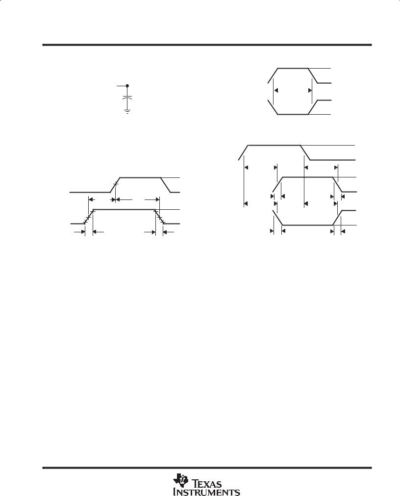
PARAMETER MEASUREMENT INFORMATION
From Output |
Test |
Under Test |
Point |
|
CL = 50 pF |
|
(see Note A) |
LOAD CIRCUIT
Reference |
|
|
50% |
VCC |
|
|
|
|
|||
Input |
|
|
|
||
|
|
|
0 V |
||
|
|
|
|
||
|
|
tsu |
th |
|
|
Data |
|
90% |
90% |
VCC |
|
Input |
50% |
50% |
|||
|
|
||||
|
10% |
|
|
10% 0 V |
|
|
|
tr |
|
tf |
VOLTAGE WAVEFORMS
SETUP AND HOLD AND INPUT RISE AND FALL TIMES
NOTES: A. CL includes probe and test-fixture capacitance.
High-Level |
|
|
|
|
|
|
|
|
50% |
|
|
|
|
|
|
|
|
|
50% |
|
|
|
VCC |
|||||||||||||||||||||||||||
|
|
|
|
|
|
|
|
|
|
|
|
|
|
|
|
|
|
|
|
|
|
|
|
|
|
|
|
|
||||||||||||||||||||||
|
|
|
|
Pulse |
|
|
|
|
|
|
|
|
|
|
|
|
|
|
|
|
|
|
|
|
0 V |
|||||||||||||||||||||||||
|
|
|
|
|
|
|
|
|
|
|
|
|
|
|
|
|
|
|
|
|
|
|
|
|
|
|
|
|
|
|
|
|
|
|||||||||||||||||
|
|
|
|
|
|
|
|
|
|
|
|
|
|
|
|
|
|
|
|
|
|
|
|
|
|
|
|
|
|
|
|
|
|
|
|
|
|
|
|
|
|
|||||||||
|
|
|
|
|
|
|
|
|
|
|
|
|
|
|
|
|
|
|
|
|
|
|
|
|
|
|
|
|
|
|
|
|
|
|
|
|
|
|
|
|
|
|||||||||
|
|
|
|
|
|
|
|
|
|
|
|
|
|
|
|
|
|
|
|
|
|
|
|
|
|
|
|
|
|
|
|
|
|
|
|
|
|
|
|
|
|
|
|
|
|
|
|
|
|
|
Low-Level |
|
|
|
|
|
|
|
|
|
|
|
|
|
|
|
tw |
|
|
|
|
|
|
|
|
|
|
|
|
|
VCC |
||||||||||||||||||||
|
|
|
|
|
|
|
|
|
|
|
|
|
|
|
|
|
|
|
|
|
|
|
|
|
|
|
|
|||||||||||||||||||||||
|
|
|
|
|
|
|
|
50% |
|
|
|
|
|
|
|
|
|
50% |
|
|
|
|||||||||||||||||||||||||||||
|
|
|
|
|
|
|
|
|
|
|
|
|
|
|
|
|
|
|
|
|||||||||||||||||||||||||||||||
|
|
|
|
Pulse |
|
|
|
|
|
|
|
|
|
|
|
|
|
|
|
|
|
|
|
|
0 V |
|||||||||||||||||||||||||
|
|
|
|
|
|
|
|
|
|
|
|
|
|
|
|
|
|
|
|
|
|
|
|
|
|
|
|
|
|
|
|
|
|
|
|
|
|
|
|
|
|
|||||||||
|
|
|
|
|
|
|
|
|
|
|
|
|
|
VOLTAGE WAVEFORMS |
|
|
|
|
|
|
|
|
|
|||||||||||||||||||||||||||
|
|
|
|
|
|
|
|
|
|
|
|
|
|
|
PULSE DURATIONS |
|
|
|
|
|
|
|
|
|
||||||||||||||||||||||||||
Input |
|
|
|
|
50% |
|
|
|
|
|
|
|
|
|
|
|
|
|
|
|
|
|
|
|
50% |
|
|
|
|
|
|
|
|
|
|
|
|
VCC |
||||||||||||
|
|
|
|
|
|
|
|
|
|
|
|
|
|
|
|
|
|
|
|
|
|
|
|
|
|
|
|
|
|
|
|
|
|
|
|
|
|
|
|
|
|
|
|
|
|
|
|
|
|
0 V |
|
|
|
|
|
|
|
|
|
|
|
|
|
|
|
|
|
|
|
|
|
|
|
|
|
|
|
|
|
|
|
|
|
|
|
|
|
|
|
|
|
|
|||||||||
|
|
|
|
|
|
|
|
|
|
|
|
|
|
|
|
|
|
|
|
|
|
|
|
|
|
|
|
|
|
|
|
|
|
|
|
|
|
|
|
|
|
|
|
|
|
|
||||
In-Phase |
|
|
|
|
|
|
|
|
|
tPLH |
|
|
|
|
|
|
|
|
|
|
|
|
|
|
|
|
|
|
|
|
tPHL |
|
|
|
|
|
|
|
|
|
|
VOH |
||||||||
|
|
|
|
|
|
|
|
|
|
|
|
|
|
|
|
|
|
|
|
|
|
|
|
|
|
|
|
|
|
|
|
|
|
|
|
|
|
|||||||||||||
|
|
|
|
|
|
|
|
|
|
|
|
|
|
|
|
|
|
|
|
|
|
|
|
|
|
|
|
|
|
|
|
|
|
|
|
|
|
|
|
|
|
|
|
|
|
|||||
|
|
|
|
|
|
|
|
|
|
|
|
|
|
|
|
|
|
|
|
|
|
|
|
|
|
|
|
|
|
|
|
|
|
|
|
|
|
|
|
|
||||||||||
Output |
|
|
|
|
|
|
|
|
50% |
|
|
|
|
|
90% |
90% |
|
|
|
|
|
50% |
||||||||||||||||||||||||||||
|
|
|
|
|
|
|
|
|
|
|
|
|
|
|
||||||||||||||||||||||||||||||||||||
|
|
|
|
|
|
|
|
|
|
|
|
|
|
|
|
|
|
|
|
|
|
|
|
|
|
|
|
|
|
|
|
|
|
|
||||||||||||||||
|
|
|
|
|
|
|
|
|
|
|
|
10% |
|
|
|
|
|
|
|
|
|
|
|
|
|
|
|
|
|
|
|
|
|
|
|
|
|
|
|
|
|
|
|
|
10% V |
|||||
|
|
|
|
|
|
|
|
|
|
|
|
|
|
|
|
|
|
|
|
|
|
|
|
|
|
|
|
|
|
|
|
|
|
|
|
|
|
|
|
|
|
|
|
|||||||
|
|
|
|
|
|
|
|
|
|
|
|
|
|
|
|
|
|
|
|
|
|
|
|
|
|
|
|
tr |
|
|
|
|
|
|
|
|
|
|
|
|
|
|
|
|
|
|
|
|
|
OL |
|
|
|
|
|
|
|
|
|
|
|
|
|
|
|
|
|
|
|
|
|
|
|
|
|
|
|
|
|
|
|
|
|
|
|
|
|
|
|
|
|
|
|
|
|
|
|
|
|
tf |
|
|
|
|
|
|
|
|
|
|
|
|
|
|
|
|
|
|
|
|
|
|
|
|
|
|
|
|
|
|
|
|
|
|
|
|
|
|
|
|
|
|
|
|
|
|
|
|
|
|||
|
|
|
|
|
|
|
|
|
|
|
|
tPHL |
|
|
|
|
|
|
|
|
|
|
|
|
|
|
|
|
|
|
|
|
|
tPLH |
|
|
|
|
|
|
|
|
|
VOH |
||||||
|
|
|
|
|
|
|
|
|
|
|
|
|
|
|
|
|
|
|
|
|
|
|
|
|
|
|
|
|
|
|
|
|
|
|
|
|
|
|||||||||||||
|
|
|
|
|
|
|
|
|
|
|
|
|
|
|
|
|
|
|
|
|
|
|
|
|
|
|
|
|
|
|
|
|
|
|
|
|
|
|
|
|
|
|
|
|
|
|
|
|
|
|
Out-of-Phase |
|
|
|
|
|
|
|
|
90% |
|
|
|
|
|
|
|
50% |
|
50% |
|
|
|
|
|
90% |
|||||||||||||||||||||||||
|
|
|
|
|
|
|
|
|
|
|
|
|
|
|
|
|
|
|
|
|
|
|
|
|
|
|
|
|
||||||||||||||||||||||
Output |
|
|
|
|
|
|
|
|
|
|
|
|
|
|
|
|
|
|
|
|
10% |
10% |
|
|
|
|
|
|
|
|
|
|
VOL |
|||||||||||||||||
|
|
|
|
|
|
|
|
|
|
|
|
|
|
|
|
|
|
|
|
|
|
|
|
|
|
|
|
|||||||||||||||||||||||
|
|
|
|
|
|
|
|
|
|
|
|
|
|
|
|
|
|
|
|
|
|
|
|
|
|
|
|
|
|
|
|
|||||||||||||||||||
|
|
|
|
|
|
|
|
|
|
|
|
|
|
|
|
|
|
|
|
|
|
|
|
|
|
|
|
|
|
|
|
|
|
|
|
|
|
|
|
|
|
|
|
|
|
|
|
|
|
|
|
|
|
|
|
|
|
|
|
|
|
|
|
|
|
|
|
|
|
|
|
|
|
|
|
|
|
|
tf |
|
|
|
|
|
|
|
|
|
|
|
|
|
|
|
|
|
|
|
|
|
tr |
|
|
|
|
|
|
|
|
|
|
|
|
|
|
|
|
|
|
|
|
|
|
|
|
|
|
|
|
|
|
|
|
|
|
|
|
|
|
|
|
|
|
|
|
|
|
|
|
|
||
VOLTAGE WAVEFORMS
PROPAGATION DELAY AND OUTPUT TRANSITION TIMES
B.Phase relationships between waveforms were chosen arbitrarily. All input pulses are supplied by generators having the following characteristics: PRR ≤ 1 MHz, ZO = 50 Ω, tr = 6 ns, tf = 6 ns.
C.For clock inputs, fmax is measured when the input duty cycle is 50%.
D.The outputs are measured one at a time with one input transition per measurement.
E.tPLH and tPHL are the same as tpd.
Figure 1. Load Circuit and Voltage Waveforms
POST OFFICE BOX 655303 • DALLAS, TEXAS 75265 |
9 |

SN54HC161, SN74HC161
4 BIT SYNCHRONOUS BINARY COUNTERS
SCLS297D − JANUARY 1996 − REVISED SEPTEMBER 2003
APPLICATION INFORMATION
n-bit synchronous counters
This application demonstrates how the look-ahead carry circuit can be used to implement a high-speed n-bit counter. The ’HC161 devices count in binary. Virtually any count mode (modulo-N, N1-to-N2, N1-to-maximum) can be used with this fast look-ahead circuit.
The application circuit shown in Figure 2 is not valid for clock frequencies above 18 MHz (at 25°C and 4.5-V VCC). The reason for this is that there is a glitch that is produced on the second stage’s RCO and every succeeding stage’s RCO. This glitch is common to all HC vendors that Texas Instruments has evaluated, in addition to the bipolar equivalents (LS, ALS, AS).
10 |
POST OFFICE BOX 655303 • DALLAS, TEXAS 75265 |