

PIC18F8722 FAMILY
1.3Details on Individual Family Members
Devices in the PIC18F8722 family are available in 64-pin and 80-pin packages. Block diagrams for the two groups are shown in Figure 1-1 and Figure 1-2.
The devices are differentiated from each other in five ways:
1.Flash program memory (48 Kbytes for PIC18F6527/8527 devices, 64 Kbytes for PIC18F6622/8622 devices, 96 Kbytes for PIC18F6627/8627 devices and 128 Kbytes for PIC18F6722/8722).
2.A/D channels (12 for 64-pin devices, 16 for 80-pin devices).
3.I/O ports (7 bidirectional ports on 64-pin devices, 9 bidirectional ports on 80-pin devices).
4.External Memory Bus, configurable for 8 and 16-bit operation, is available on PIC18F8527/ 8622/8627/8722 devices.
All other features for devices in this family are identical. These are summarized in Table 1-2 and Table 1-2.
The pinouts for all devices are listed in Table 1-3 and Table 1-4.
Like all Microchip PIC18 devices, members of the PIC18F8722 family are available as both standard and low-voltage devices. Standard devices with Enhanced Flash memory, designated with an “F” in the part number (such as PIC18F6627), accommodate an operating VDD range of 4.2V to 5.5V. Low-voltage parts, designated by “LF” (such as PIC18LF6627), function over an extended VDD range of 2.0V to 5.5V.
TABLE 1-1: |
DEVICE FEATURES (PIC18F6527/6622/6627/6722) |
|
|||
Features |
|
PIC18F6527 |
PIC18F6622 |
PIC18F6627 |
PIC18F6722 |
|
|
|
|
|
|
|
|
|
|
|
|
Operating Frequency |
DC – 40 MHz |
DC – 40 MHz |
DC – 40 MHz |
DC – 40 MHz |
|
|
|
|
|
|
|
Program Memory (Bytes) |
48K |
64K |
96K |
128K |
|
|
|
|
|
|
|
Program Memory (Instructions) |
24576 |
32768 |
49152 |
65536 |
|
|
|
|
|
|
|
Data Memory (Bytes) |
3936 |
3936 |
3936 |
3936 |
|
|
|
|
|
|
|
Data EEPROM Memory (Bytes) |
1024 |
1024 |
1024 |
1024 |
|
|
|
|
|
|
|
Interrupt Sources |
|
28 |
28 |
28 |
28 |
|
|
|
|
|
|
I/O Ports |
|
Ports A, B, C, D, E, F, G |
Ports A, B, C, D, E, F, G |
Ports A, B, C, D, E, F, G |
Ports A, B, C, D, E, F, G |
|
|
|
|
|
|
Timers |
|
5 |
5 |
5 |
5 |
|
|
|
|
|
|
Capture/Compare/PWM |
2 |
2 |
2 |
2 |
|
Modules |
|
|
|
|
|
|
|
|
|
|
|
Enhanced Capture/Compare/ |
3 |
3 |
3 |
3 |
|
PWM Modules |
|
|
|
|
|
|
|
|
|
|
|
Enhanced USART |
|
2 |
2 |
2 |
2 |
|
|
|
|
|
|
Serial Communications |
MSSP, |
MSSP, |
MSSP, |
MSSP, |
|
|
|
Enhanced USART |
Enhanced USART |
Enhanced USART |
Enhanced USART |
|
|
|
|
|
|
Parallel Communications (PSP) |
Yes |
Yes |
Yes |
Yes |
|
|
|
|
|
|
|
10-bit Analog-to-Digital Module |
12 Input Channels |
12 Input Channels |
12 Input Channels |
12 Input Channels |
|
|
|
|
|
|
|
Resets (and Delays) |
|
POR, BOR, |
POR, BOR, |
POR, BOR, |
POR, BOR, |
|
|
RESET Instruction, |
RESET Instruction, |
RESET Instruction, |
RESET Instruction, |
|
|
Stack Full, Stack |
Stack Full, Stack |
Stack Full, Stack |
Stack Full, Stack |
|
|
Underflow (PWRT, OST), |
Underflow (PWRT, OST), |
Underflow (PWRT, OST), |
Underflow (PWRT, OST), |
|
|
MCLR (optional), WDT |
MCLR (optional), WDT |
MCLR (optional), WDT |
MCLR (optional), WDT |
|
|
|
|
|
|
Programmable |
|
Yes |
Yes |
Yes |
Yes |
High/Low-Voltage Detect |
|
|
|
|
|
|
|
|
|
|
|
Programmable Brown-out |
Yes |
Yes |
Yes |
Yes |
|
Reset |
|
|
|
|
|
|
|
|
|
|
|
Instruction Set |
|
75 Instructions; |
75 Instructions; |
75 Instructions; |
75 Instructions; |
|
|
83 with Extended |
83 with Extended |
83 with Extended |
83 with Extended |
|
|
Instruction Set enabled |
Instruction Set enabled |
Instruction Set enabled |
Instruction Set enabled |
|
|
|
|
|
|
Packages |
|
64-pin TQFP |
64-pin TQFP |
64-pin TQFP |
64-pin TQFP |
|
|
|
|
|
|
2004 Microchip Technology Inc.
Preliminary
DS39646B-page 9

PIC18F8722 FAMILY
TABLE 1-2: |
DEVICE FEATURES (PIC18F8527/8622/8627/8722) |
|
|||
Features |
|
PIC18F8527 |
PIC18F8622 |
PIC18F8627 |
PIC18F8722 |
|
|
|
|
|
|
|
|
|
|
|
|
Operating Frequency |
DC – 40 MHz |
DC – 40 MHz |
DC – 40 MHz |
DC – 40 MHz |
|
|
|
|
|
|
|
Program Memory (Bytes) |
48K |
64K |
96K |
128K |
|
|
|
|
|
|
|
Program Memory (Instructions) |
24576 |
32768 |
49152 |
65536 |
|
|
|
|
|
|
|
Data Memory (Bytes) |
3936 |
3936 |
3936 |
3936 |
|
|
|
|
|
|
|
Data EEPROM Memory (Bytes) |
1024 |
1024 |
1024 |
1024 |
|
|
|
|
|
|
|
Interrupt Sources |
|
29 |
29 |
29 |
29 |
|
|
|
|
|
|
I/O Ports |
|
Ports A, B, C, D, E, |
Ports A, B, C, D, E, |
Ports A, B, C, D, E, |
Ports A, B, C, D, E, |
|
|
F, G, H, J |
F, G, H, J |
F, G, H, J |
F, G, H, J |
|
|
|
|
|
|
Timers |
|
5 |
5 |
5 |
5 |
|
|
|
|
|
|
Capture/Compare/PWM |
2 |
2 |
2 |
2 |
|
Modules |
|
|
|
|
|
|
|
|
|
|
|
Enhanced Capture/Compare/ |
3 |
3 |
3 |
3 |
|
PWM Modules |
|
|
|
|
|
|
|
|
|
|
|
Enhanced USART |
|
2 |
2 |
2 |
2 |
|
|
|
|
|
|
Serial Communications |
MSSP, |
MSSP, |
MSSP, |
MSSP, |
|
|
|
Enhanced USART |
Enhanced USART |
Enhanced USART |
Enhanced USART |
|
|
|
|
|
|
Parallel Communications |
Yes |
Yes |
Yes |
Yes |
|
(PSP) |
|
|
|
|
|
|
|
|
|
|
|
10-bit Analog-to-Digital Module |
16 Input Channels |
16 Input Channels |
16 Input Channels |
16 Input Channels |
|
|
|
|
|
|
|
Resets (and Delays) |
|
POR, BOR, |
POR, BOR, |
POR, BOR, |
POR, BOR, |
|
|
RESET Instruction, |
RESET Instruction, |
RESET Instruction, |
RESET Instruction, |
|
|
Stack Full, Stack |
Stack Full, Stack |
Stack Full, Stack |
Stack Full, Stack |
|
|
Underflow (PWRT, OST), |
Underflow (PWRT, OST), |
Underflow (PWRT, OST), |
Underflow (PWRT, OST), |
|
|
MCLR (optional), WDT |
MCLR (optional), WDT |
MCLR (optional), WDT |
MCLR (optional), WDT |
|
|
|
|
|
|
Programmable |
|
Yes |
Yes |
Yes |
Yes |
High/Low-Voltage Detect |
|
|
|
|
|
|
|
|
|
|
|
Programmable Brown-out |
Yes |
Yes |
Yes |
Yes |
|
Reset |
|
|
|
|
|
|
|
|
|
|
|
Instruction Set |
|
75 Instructions; |
75 Instructions; |
75 Instructions; |
75 Instructions; |
|
|
83 with Extended |
83 with Extended |
83 with Extended |
83 with Extended |
|
|
Instruction Set enabled |
Instruction Set enabled |
Instruction Set enabled |
Instruction Set enabled |
|
|
|
|
|
|
Packages |
|
80-pin TQFP |
80-pin TQFP |
80-pin TQFP |
80-pin TQFP |
|
|
|
|
|
|
DS39646B-page 10 |
Preliminary |
2004 Microchip Technology Inc. |
PIC18F8722 FAMILY
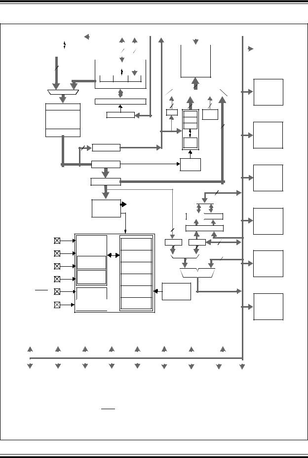
FIGURE 1-1: PIC18F6527/6622/6627/6722 (64-PIN) BLOCK DIAGRAM
|
|
|
|
|
|
|
|
|
|
|
|
Data Bus<8> |
|
|
|
|
|
|
|
|
||||||
|
Table Pointer<21> |
|
|
|
|
|
|
|
|
|
|
|
|
|
|
|
|
|
|
|
|
|
|
|
|
PORTA |
|
|
|
|
|
|
|
|
|
|
|
|
|
|
|
|
|
|
|
|
|
|
|
|
|
|
|
|
inc/dec logic |
|
|
|
|
|
|
|
8 |
|
|
8 |
|
|
|
|
Data Latch |
|
|
|
RA0:RA7(1) |
|||||
|
|
|
|
|
|
|
|
|
|
|
Data Memory |
|||||||||||||||
|
|
|
|
|
|
|
|
|
|
|
|
|
|
|
|
|
|
|
|
|||||||
|
|
|
|
|
|
|
|
|
|
|
|
|
|
|
|
|
|
|
|
|||||||
|
|
|
|
|
|
|
|
|
|
|
|
|
|
|
|
|
|
|
(3.9 Kbytes) |
|
||||||
|
|
|
|
|
|
|
|
|
|
|
|
|
|
|
|
|
|
|
|
|||||||
21 |
|
|
|
|
PCLATU |
PCLATH |
|
|
|
|
|
|
|
|
|
|||||||||||
|
|
|
|
|
|
|
|
|
|
|
|
|
|
|
|
|
|
|
|
|||||||
|
|
|
|
|
|
|
|
|
|
|
|
|
|
|
|
|
|
|
|
|
|
|
|
|
|
|
20 |
|
|
|
|
|
|
|
|
|
|
|
|
|
|
|
|
Address Latch |
|||||||||
|
|
|
|
|
|
|
|
|
|
|
|
|
|
|
|
|||||||||||
|
PCU |
PCH |
PCL |
|
|
|
|
|
|
Program Counter |
|
|
12 |
|
PORTB |
||
|
|
|
|
Data Address<12> |
|
RB0:RB7(1) |
||
|
|
|
|
|
|
|
|
|
|
31 Level Stack |
4 |
12 |
4 |
|
|
||
Address Latch |
|
|
|
|
||||
Program Memory |
STKPTR |
BSR |
FSR0 |
Access |
|
|
||
|
Bank |
|
|
|||||
(48/64/96/128 |
|
|
|
|
FSR1 |
|
|
|
|
|
|
|
|
|
|
||
Kbytes) |
|
|
|
|
FSR2 |
12 |
|
PORTC |
Data Latch |
|
|
|
|
|
|
||
|
|
|
|
|
|
|
||
|
|
|
|
|
|
|
|
|
|
8 |
|
|
|
inc/dec |
|
|
RC0:RC7(1) |
|
|
|
|
logic |
|
|
|
|
|
Table Latch |
|
|
|
|
|
|
|
|
ROM Latch |
|
|
Address |
|
|
|
|
|
|
|
Decode |
|
|
|
||
Instruction Bus <16> |
|
|
|
|
|
PORTD |
||
|
|
|
|
|
|
|
|
|
|
IR |
|
|
|
|
|
|
RD0:RD7(1) |
|
|
|
State Machine |
|
|
8 |
|
|
|
Instruction |
|
|
|
|
|
||
|
Control Signals |
|
|
|
|
|
||
|
Decode and |
|
|
|
|
|
||
|
Control |
|
|
PRODH PRODL |
PORTE |
|||
|
|
|
|
|
||||
|
|
|
|
|
8 x 8 Multiply |
|
RE0:RE7(1) |
|
|
|
|
|
3 |
|
|
||
|
|
|
|
|
|
|
8 |
|
|
|
|
|
|
|
|
|
|
OSC1(3) |
Internal |
|
Power-up |
BITOP |
W |
|
|
|
|
Oscillator |
|
Timer |
8 |
|
8 |
8 |
|
|
Block |
|
|
|
||||
OSC2(3) |
|
Oscillator |
|
|
|
|||
|
|
|
|
|
|
|
||
|
INTRC |
Start-up Timer |
|
8 |
|
8 |
PORTF |
|
|
Oscillator |
|
Power-on |
|
|
|
||
T1OSI |
|
|
|
|
RF0:RF7(1) |
|||
|
|
|
|
|
||||
|
|
Reset |
|
|
|
|
||
|
8 MHz |
|
|
ALU<8> |
|
|
||
|
|
Watchdog |
|
|
|
|||
T1OSO |
Oscillator |
|
|
|
|
|
|
|
|
Timer |
|
|
8 |
|
|
||
|
|
|
Precision |
|
|
|||
|
|
|
Brown-out |
|
|
|||
|
Single-Supply |
|
|
|
|
|||
MCLR(2) |
|
Band Gap |
|
|
|
|||
|
Reset |
|
|
|
||||
|
Programming |
|
Reference |
|
|
|
||
|
|
Fail-Safe |
|
|
PORTG |
|||
VDD, VSS |
In-Circuit |
|
|
|
|
|
||
Debugger |
Clock Monitor |
|
|
|
|
RG0:RG5(1) |
||
|
|
|
|
|
|
|
||
|
|
|
|
|
|
|
|
|
BOR |
|
ADC |
|
Timer0 |
|
Timer1 |
|
Timer2 |
|
Timer3 |
|
Timer4 |
|
Comparators |
|
|
|||||||||||||||||||||||||
HLVD |
|
10-bit |
|
|
|
|
|
|
|
|
|||||||||||||||||||||||||||||||
|
|
|
|
|
|
|
|
|
|
|
|
|
|
|
|
|
|
|
|
|
|
|
|
|
|
|
|
|
|
|
|
|
|
|
|
|
|
|
|
|
|
|
|
|
|
|
|
|
|
|
|
|
|
|
|
|
|
|
|
|
|
|
|
|
|
|
|
|
|
|
|
|
|
|
|
|
|
|
|
|
|
|
|
|
|
|
|
|
|
|
|
|
|
|
|
|
|
|
|
|
|
|
|
|
|
|
|
|
|
|
|
|
|
|
|
|
|
|
|
|
|
|
|
|
|
|
|
|
|
|
|
|
|
|
|
|
|
|
|
|
|
|
|
|
|
|
|
|
|
|
|
|
|
|
|
|
|
|
|
|
|
|
|
|
|
|
|
|
ECCP1 |
|
|
ECCP2 |
|
ECCP3 |
|
CCP4 |
|
|
CCP5 |
|
EUSART1 |
|
EUSART2 |
|
MSSP1 |
|
MSSP2 |
|
|
|
|
|
|
|
|
|
|
|
|
|
|
|
|
|
|
|
|
Note 1: |
See Table 1-3 for I/O port pin descriptions. |
|
|
|
|
|
|
|
|
|
|||||||||
2:RG5 is only available when MCLR functionality is disabled.
3:OSC1/CLKI and OSC2/CLKO are only available in select oscillator modes and when these pins are not being used as digital I/O. Refer to Section 2.0 “Oscillator Configurations” for additional information.
2004 Microchip Technology Inc.
Preliminary
DS39646B-page 11
PIC18F8722 FAMILY
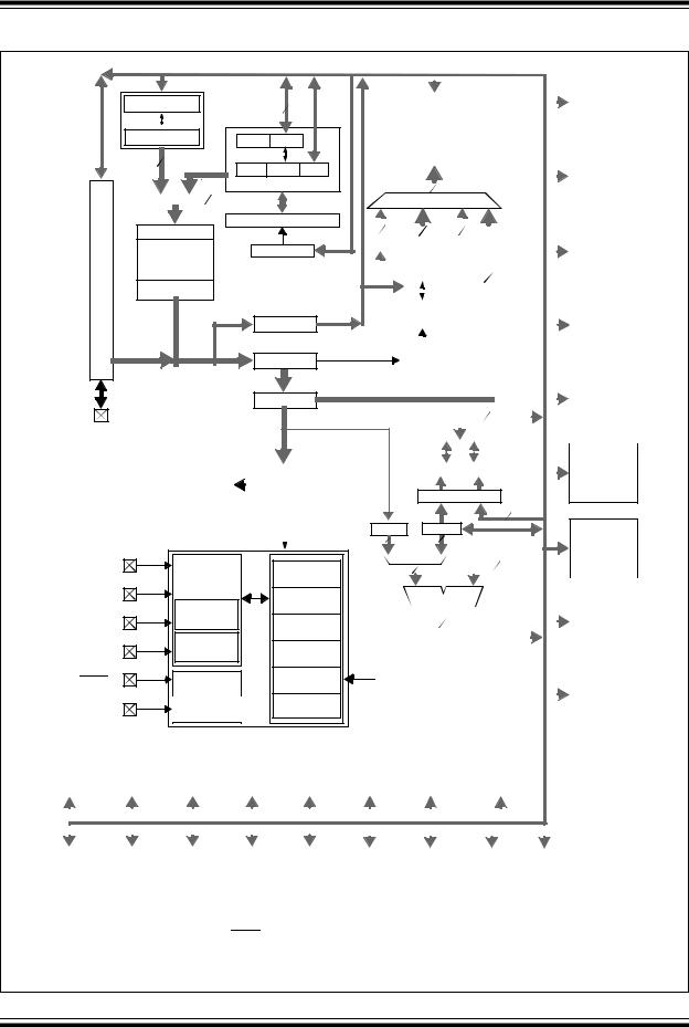
FIGURE 1-2: PIC18F8527/8622/8627/8722 (80-PIN) BLOCK DIAGRAM
Data Bus<8>
|
Table Pointer<21> |
|
8 |
8 |
|
|
|
||
|
inc/dec logic |
PCLATU PCLATH |
|
|
|
|
|
||
|
21 |
20 |
|
|
|
|
PCU |
PCH |
PCL |
|
|
Program Counter |
||
|
|
31 Level Stack |
||
Interface |
Address Latch |
|
|
|
Program Memory |
STKPTR |
|
||
|
|
|||
|
(48/64/96/128 |
|
||
|
|
|
||
Bus |
Kbytes) |
|
|
|
Data Latch |
|
|
|
|
System |
|
|
|
|
|
8 |
Table Latch |
||
|
|
|
|
|
|
|
|
ROM Latch |
|
|
Instruction Bus <16> |
|
|
|
|
|
|
IR |
|
|
AD15:AD0, A19:A16 |
|
|
|
|
(Multiplexed with PORTD, |
|
|
|
|
PORTE and PORTH) |
|
|
|
State Machine |
|
|
Instruction |
||
Control Signals |
|
Decode & |
|||
Control |
|||||
|
|
|
|||
|
|
|
|
|
|
|
|
|
|
|
|
OSC1(3) |
Internal |
Power-up |
|
|
Oscillator |
Timer |
|
OSC2(3) |
Block |
Oscillator |
|
|
|||
|
INTRC |
Start-up Timer |
|
T1OSI |
Oscillator |
Power-on |
|
|
Reset |
||
|
8 MHz |
||
|
Watchdog |
||
T1OSO |
Oscillator |
||
Timer |
|||
|
|
||
MCLR(2) |
Single-Supply |
Brown-out |
|
Reset |
|||
|
Programming |
||
|
Fail-Safe |
||
VDD, VSS |
In-Circuit |
||
Clock Monitor |
|||
Debugger |
|||
|
|
|
|
|
|
|
|
|
|
|
|
|
|
|
|
|
|
|
|
|
|
|
|
|
|
|
|
|
|
|
PORTA |
|
|
|
|
|
|
|
|
|
|
|
|
|
|
|
|
|
|
|
|
|
|
|
|
|
|
|
|
|
|
|
|
|
|
|
Data Latch |
|
|
|
|
|
|
|
|
|
|
|
|
|
RA0:RA7(1) |
||||||||||
|
|
|
|
Data Memory |
|
|
|
|
|
|
|
|
|
|
|
|
|
||||||||||||
|
|
|
|
|
|
|
|
|
|
|
|
|
|
|
|
|
|
||||||||||||
|
|
|
|
|
(3.9 Kbytes) |
|
|
|
|
|
|
|
|
|
|
|
|
|
|
||||||||||
|
|
|
|
|
|
|
|
|
|
|
|
|
|
|
|
|
|
|
|||||||||||
|
|
|
|
|
|
|
|
|
|
|
|
|
|
|
|
|
|
|
|
|
|
|
|
|
|
|
|
||
|
|
|
|
Address Latch |
|
|
|
|
|
|
|
|
|
|
|
|
|
PORTB |
|||||||||||
|
|
|
|
|
|
|
|
|
|
|
|
|
|
|
|
|
|
|
|
|
|
|
|
|
|
|
|
|
|
|
|
|
|
|
|
|
|
|
|
|
12 |
|
|
|
|
|
|
|
|
|
|
|
|
|
|
|
|
RB0:RB7(1) |
|
|
|
|
|
|
|
|
|
|
|
|
|
|
|
|
|
|
|
|
|
|
|
|
|
|
|
|
|||
|
|
Data Address<12> |
|
|
|
|
|
|
|||||||||||||||||||||
|
|
|
|
|
|
|
|
|
|
|
|
|
|
|
|
|
|
|
|
|
|
|
|
|
|
|
|
|
|
|
4 |
|
|
|
12 |
|
|
|
|
|
4 |
|
|
|
|
|
|
|
|
|
|
|
PORTC |
||||||
BSR |
|
|
|
FSR0 |
|
|
Access |
|
|
|
|
|
|
|
|
|
|
||||||||||||
|
|
|
|
|
|
|
|
|
|
|
|
|
Bank |
|
|
|
|
|
|
|
|
|
|
RC0:RC7(1) |
|||||
|
|
|
|
|
FSR1 |
|
|
|
|
|
|
|
|
|
|
|
|
|
|||||||||||
|
|
|
|
|
|
|
|
|
|
|
|
|
|
|
|
|
|
|
|
|
|
|
|
||||||
|
|
|
|
|
FSR2 |
|
|
|
|
|
|
12 |
|
|
|
|
|
|
|
|
|
||||||||
|
|
|
|
|
|
|
|
|
|
|
|
|
|
|
|
|
|
|
|
|
|
|
|
|
|||||
|
|
|
|
|
|
|
|
|
|
|
|
|
|
|
|
|
|
|
|
|
|
|
|
|
|
|
|
|
|
|
|
|
|
|
|
|
|
|
|
|
|
|
|
|
|
|
|
|
|
|
|
|
|
|
|
|
|
|
|
|
|
|
|
|
inc/dec |
|
|
|
|
|
|
|
|
|
|
|
|
|
|
|
|
|
|
|
PORTD |
||||
|
|
|
|
|
logic |
|
|
|
|
|
|
|
|
|
|
|
|
|
|
|
|
|
|
|
|||||
|
|
|
|
|
|
|
|
|
|
|
|
|
|
|
|
|
|
|
|
|
|
|
|
|
|
|
|
|
RD0:RD7(1) |
|
|
|
|
|
|
|
|
|
|
|
|
|
|
|
|
|
|
|
|
|
|
|
|
|
|
|
|
|
|
|
|
|
|
|
|
|
|
|
|
|
|
|
|
|
|
|
|
|
|
|
|
|
|
|
|
||||
|
|
|
|
|
|
|
|
|
|
|
|
|
|
|
|
|
|
|
|
|
|
|
|
|
|
||||
|
|
|
|
Address |
|
|
|
|
|
|
|
|
|
|
|
|
|
|
|
|
|||||||||
|
|
|
|
|
|
|
|
|
|
|
|
|
|
|
|
|
|
|
|
|
|
||||||||
|
|
|
|
|
Decode |
|
|
|
|
|
|
|
|
|
|
|
|
|
|
|
|
|
|
|
|||||
|
|
|
|
|
|
|
|
|
|
|
|
|
|
|
|
|
|
|
|
|
|
|
|
|
|
|
|
|
PORTE |
|
|
|
|
|
|
|
|
|
|
|
|
|
|
|
|
|
|
|
|
|
|
|
|
|
|
|
|
|
RE0:RE7(1) |
|
|
|
|
|
|
|
|
|
|
|
|
|
|
|
|
8 |
|
|
|
|
|
|
|
|
|||||
|
|
|
|
|
|
|
|
|
|
|
|
|
|
|
|
|
|
|
|
|
|
|
|
|
|
|
|
|
|
|
|
|
|
|
|
|
|
|
|
|
|
|
|
|
|
|
|
|
|
|
|
|
|
|
|
|
|
|
|
|
|
|
|
|
|
|
|
|
|
|
|
|
|
|
|
|
|
|
|
|
|
|
|
|
|
|
|
|
PORTF |
|
|
|
|
|
|
|
|
|
|
|
|
|
|
|
|
|
|
|
|
|
|
|
|
|
|
|
|
|
|
|
|
|
|
|
|
|
|
|
|
|
|
|
|
|
|
|
|
|
|
|
|
|
|
|
|
|
|
|
|
|
|
|
|
|
|
PRODH |
|
PRODL |
|||||||||||||||||||||
|
|
|
|
|
|
|
|
|
|
|
|
|
|
|
|
|
|
|
|
|
|
|
|
|
|
|
|
|
|
|
8 x 8 Multiply |
|
RF0:RF7(1) |
|
3 |
|
|
||
|
|
8 |
||
|
|
|
||
BITOP |
W |
8 |
PORTG |
|
8 |
8 |
|||
|
||||
|
|
|
RG0:RG5(1) |
|
|
8 |
|
|
|
8 |
|
|
|
|
|
|
|
|
|
|
|
|
|
|
|
||
|
|
ALU<8> |
|
|
|
|
|
|
|
||
|
|
|
|
|
|
|
|
PORTH |
|||
|
|
|
|
8 |
|
|
|
|
|
|
|
|
|
|
|
|
|
|
|||||
|
|
|
|
|
|
|
|
|
|
RH0:RH7(1) |
|
|
|
|
|
|
|
|
|
|
|
|
|
|
|
|
|
|
|
|
|
|
|||
|
|
|
|
|
|
|
|
|
|
|
|
Precision |
|
|
|
|
|
|
|
|
|
||
Band Gap |
|
|
|
|
|
|
|
PORTJ |
|||
Reference |
|
|
|
|
|
|
|
RJ0:RJ7(1) |
|||
|
|
|
|
|
|
|
|
|
|
|
|
|
|
|
|
|
|
|
|
|
|
|
|
|
|
|
|
|
|
|
|
|
|
|
|
BOR |
|
ADC |
|
Timer0 |
|
Timer1 |
|
Timer2 |
|
Timer3 |
|
Timer4 |
|
Comparators |
|
|
|||||||||||||||||||||||||
HLVD |
|
10-bit |
|
|
|
|
|
|
|
|
|||||||||||||||||||||||||||||||
|
|
|
|
|
|
|
|
|
|
|
|
|
|
|
|
|
|
|
|
|
|
|
|
|
|
|
|
|
|
|
|
|
|
|
|
|
|
|
|
|
|
|
|
|
|
|
|
|
|
|
|
|
|
|
|
|
|
|
|
|
|
|
|
|
|
|
|
|
|
|
|
|
|
|
|
|
|
|
|
|
|
|
|
|
|
|
|
|
|
|
|
|
|
|
|
|
|
|
|
|
|
|
|
|
|
|
|
|
|
|
|
|
|
|
|
|
|
|
|
|
|
|
|
|
|
|
|
|
|
|
|
|
|
|
|
|
|
|
|
|
|
|
|
|
|
|
|
|
|
|
|
|
|
|
|
|
|
|
|
|
|
|
|
|
|
|
|
|
ECCP1 |
|
|
ECCP2 |
|
ECCP3 |
|
CCP4 |
|
CCP5 |
|
EUSART1 |
|
EUSART2 |
|
MSSP1 |
|
MSSP2 |
|
|
|
|
|
|
|
|
|
|
|
|
|
|
|
|
|
|
|
Note 1: |
See Table 1-4 for I/O port pin descriptions. |
|
|
|
|
|
|
|
||||||||||
2:RG5 is only available when MCLR functionality is disabled.
3:OSC1/CLKI and OSC2/CLKO are only available in select oscillator modes and when these pins are not being used as digital I/O. Refer to Section 2.0 “Oscillator Configurations” for additional information.
DS39646B-page 12 |
Preliminary |
2004 Microchip Technology Inc. |

|
|
|
|
|
|
|
|
|
|
|
PIC18F8722 FAMILY |
|||
|
|
|
|
|
|
|
|
|
|
|
|
|
|
|
TABLE 1-3: |
PIC18F6527/6622/6627/6722 PINOUT I/O DESCRIPTIONS |
|||||||||||||
|
|
Pin Name |
|
Pin Number |
Pin |
Buffer |
|
|
Description |
|||||
|
|
|
|
|
|
|||||||||
|
|
|
TQFP |
Type |
Type |
|
|
|||||||
|
|
|
|
|
|
|
|
|
|
|
|
|||
|
|
|
|
|
|
|
|
|
|
|
|
|
|
|
|
|
|
|
|
|
|
|
|||||||
|
|
|
|
|
|
|
|
|
|
|
|
|
|
|
|
|
|
|
|
PP |
|
7 |
|
|
Master Clear (input) or programming voltage (input). |
||||
RG5/MCLR/V |
|
|
|
|||||||||||
|
RG5 |
|
|
|
|
|
I |
ST |
Digital input. |
|
|
|||
|
MCLR |
|
|
|
|
|
|
I |
ST |
Master Clear (Reset) input. This pin is an active-low |
||||
|
|
|
|
|
|
|
|
|
|
|
Reset to the device. |
|||
|
VPP |
|
|
|
|
|
P |
|
Programming voltage input. |
|||||
|
|
|
|
|
|
|||||||||
OSC1/CLKI/RA7 |
|
39 |
|
|
Oscillator crystal or external clock input. |
|||||||||
|
OSC1 |
|
|
|
|
|
I |
ST |
Oscillator crystal input or external clock source input. |
|||||
|
|
|
|
|
|
|
|
|
|
|
ST buffer when configured in RC mode, CMOS |
|||
|
|
|
|
|
|
|
|
|
|
|
otherwise. |
|
|
|
|
CLKI |
|
|
|
|
|
I |
CMOS |
External clock source input. Always associated |
|||||
|
|
|
|
|
|
|
|
|
|
|
with pin function OSC1. (See related OSC1/CLKI, |
|||
|
|
|
|
|
|
|
|
|
|
|
OSC2/CLKO pins.) |
|||
|
RA7 |
|
|
|
|
|
I/O |
TTL |
General purpose I/O pin. |
|||||
|
|
|
|
|
|
|||||||||
OSC2/CLKO/RA6 |
|
40 |
|
|
Oscillator crystal or clock output. |
|||||||||
|
OSC2 |
|
|
|
|
|
O |
— |
Oscillator crystal output. Connects to crystal or |
|||||
|
|
|
|
|
|
|
|
|
|
|
resonator in Crystal Oscillator mode. |
|||
|
CLKO |
|
|
|
|
|
O |
— |
In RC mode, OSC2 pin outputs CLKO, which has |
|||||
|
|
|
|
|
|
|
|
|
|
|
1/4 the frequency of OSC1 and denotes the |
|||
|
|
|
|
|
|
|
|
|
|
|
instruction cycle rate. |
|||
|
RA6 |
|
|
|
|
|
I/O |
TTL |
General purpose I/O pin. |
|||||
|
|
|
|
|
|
|
||||||||
Legend: |
TTL = TTL compatible input |
|
|
CMOS |
= CMOS compatible input or output |
|||||||||
|
|
|
|
ST |
= |
Schmitt Trigger input with CMOS levels |
Analog |
= |
Analog input |
|||||
|
|
|
|
I |
= |
Input |
|
|
O |
= |
Output |
|||
|
|
|
|
P |
= Power |
|
|
I2C™ |
= I2C/SMBus input buffer |
|||||
Note 1: |
Default assignment for ECCP2 when configuration bit CCP2MX is set. |
|||||||||||||
2:Alternate assignment for ECCP2 when configuration bit CCP2MX is cleared.
2004 Microchip Technology Inc.
Preliminary
DS39646B-page 13

PIC18F8722 FAMILY
TABLE 1-3: |
PIC18F6527/6622/6627/6722 PINOUT I/O DESCRIPTIONS (CONTINUED) |
||||
Pin Name |
|
Pin Number |
Pin |
Buffer |
Description |
|
|
||||
|
TQFP |
Type |
Type |
||
|
|
|
|||
|
|
|
|
|
|
|
|
|
|
|
|
|
|
|
|
|
|
|
|
|
|
|
PORTA is a bidirectional I/O port. |
RA0/AN0 |
|
24 |
|
|
|
RA0 |
|
|
I/O |
TTL |
Digital I/O. |
AN0 |
|
|
I |
Analog |
Analog input 0. |
RA1/AN1 |
|
23 |
|
|
|
RA1 |
|
|
I/O |
TTL |
Digital I/O. |
AN1 |
|
|
I |
Analog |
Analog input 1. |
RA2/AN2/VREF- |
|
22 |
|
|
|
RA2 |
|
|
I/O |
TTL |
Digital I/O. |
AN2 |
|
|
I |
Analog |
Analog input 2. |
VREF- |
|
|
I |
Analog |
A/D reference voltage (low) input. |
RA3/AN3/VREF+ |
|
21 |
|
|
|
RA3 |
|
|
I/O |
TTL |
Digital I/O. |
AN3 |
|
|
I |
Analog |
Analog input 3. |
VREF+ |
|
|
I |
Analog |
A/D reference voltage (high) input. |
RA4/T0CKI |
|
28 |
|
|
|
RA4 |
|
|
I/O |
ST |
Digital I/O. |
T0CKI |
|
|
I |
ST |
Timer0 external clock input. |
RA5/AN4/HLVDIN |
27 |
|
|
|
|
RA5 |
|
|
I/O |
TTL |
Digital I/O. |
AN4 |
|
|
I |
Analog |
Analog input 4. |
HLVDIN |
|
|
I |
Analog |
High/Low-Voltage Detect input. |
RA6 |
|
|
|
|
See the OSC2/CLKO/RA6 pin. |
RA7 |
|
|
|
|
See the OSC1/CLKI/RA7 pin. |
|
|
|
|
|
|
Legend: |
TTL |
= TTL compatible input |
CMOS |
= CMOS compatible input or output |
||
|
ST |
= |
Schmitt Trigger input with CMOS levels |
Analog |
= |
Analog input |
|
I |
= |
Input |
O |
= |
Output |
|
P |
= Power |
I2C™ |
= I2C/SMBus input buffer |
||
Note 1: |
Default assignment for ECCP2 when configuration bit CCP2MX is set. |
|||||
2:Alternate assignment for ECCP2 when configuration bit CCP2MX is cleared.
DS39646B-page 14 |
Preliminary |
2004 Microchip Technology Inc. |

PIC18F8722 FAMILY
TABLE 1-3: PIC18F6527/6622/6627/6722 PINOUT I/O DESCRIPTIONS (CONTINUED)
Pin Name |
Pin Number |
Pin |
Buffer |
Description |
|
|
|||||
TQFP |
Type |
Type |
|||
|
|
||||
|
|
|
|
||
|
|
|
|
|
|
|
|
|
|
|
|
|
|
|
|
PORTB is a bidirectional I/O port. PORTB can be software |
|
|
|
|
|
programmed for internal weak pull-ups on all inputs. |
|
RB0/INT0/FLT0 |
48 |
|
|
|
|
RB0 |
|
I/O |
TTL |
Digital I/O. |
|
INT0 |
|
I |
ST |
External interrupt 0. |
|
FLT0 |
|
I |
ST |
PWM Fault input for ECCPx. |
|
RB1/INT1 |
47 |
|
|
|
|
RB1 |
|
I/O |
TTL |
Digital I/O. |
|
INT1 |
|
I |
ST |
External interrupt 1. |
|
RB2/INT2 |
46 |
|
|
|
|
RB2 |
|
I/O |
TTL |
Digital I/O. |
|
INT2 |
|
I |
ST |
External interrupt 2. |
|
RB3/INT3 |
45 |
|
|
|
|
RB3 |
|
I/O |
TTL |
Digital I/O. |
|
INT3 |
|
I |
ST |
External interrupt 3. |
|
RB4/KBI0 |
44 |
|
|
|
|
RB4 |
|
I/O |
TTL |
Digital I/O. |
|
KBI0 |
|
I |
TTL |
Interrupt-on-change pin. |
|
RB5/KBI1/PGM |
43 |
|
|
|
|
RB5 |
|
I/O |
TTL |
Digital I/O. |
|
KBI1 |
|
I |
TTL |
Interrupt-on-change pin. |
|
PGM |
|
I/O |
ST |
Low-Voltage ICSP™ Programming enable pin. |
|
RB6/KBI2/PGC |
42 |
|
|
|
|
RB6 |
|
I/O |
TTL |
Digital I/O. |
|
KBI2 |
|
I |
TTL |
Interrupt-on-change pin. |
|
PGC |
|
I/O |
ST |
In-Circuit Debugger and ICSP programming clock pin. |
|
RB7/KBI3/PGD |
37 |
|
|
|
|
RB7 |
|
I/O |
TTL |
Digital I/O. |
|
KBI3 |
|
I |
TTL |
Interrupt-on-change pin. |
|
PGD |
|
I/O |
ST |
In-Circuit Debugger and ICSP programming data pin. |
|
|
|
|
|
|
Legend: |
TTL |
= TTL compatible input |
CMOS |
= CMOS compatible input or output |
||
|
ST |
= |
Schmitt Trigger input with CMOS levels |
Analog |
= |
Analog input |
|
I |
= |
Input |
O |
= |
Output |
|
P |
= Power |
I2C™ |
= I2C/SMBus input buffer |
||
Note 1: |
Default assignment for ECCP2 when configuration bit CCP2MX is set. |
|||||
2:Alternate assignment for ECCP2 when configuration bit CCP2MX is cleared.
2004 Microchip Technology Inc.
Preliminary
DS39646B-page 15

PIC18F8722 FAMILY
TABLE 1-3: PIC18F6527/6622/6627/6722 PINOUT I/O DESCRIPTIONS (CONTINUED)
Pin Name |
Pin Number |
Pin |
Buffer |
Description |
|
|
|||||
TQFP |
Type |
Type |
|||
|
|
||||
|
|
|
|
||
|
|
|
|
|
|
|
|
|
|
|
|
|
|
|
|
PORTC is a bidirectional I/O port. |
|
RC0/T1OSO/T13CKI |
30 |
|
|
|
|
RC0 |
|
I/O |
ST |
Digital I/O. |
|
T1OSO |
|
O |
— |
Timer1 oscillator output. |
|
T13CKI |
|
I |
ST |
Timer1/Timer3 external clock input. |
|
RC1/T1OSI/ECCP2/P2A |
29 |
|
|
|
|
RC1 |
|
I/O |
ST |
Digital I/O. |
|
T1OSI |
|
I |
CMOS |
Timer1 oscillator input. |
|
ECCP2(1) |
|
I/O |
ST |
Enhanced Capture 2 input/Compare 2 output/ |
|
P2A(1) |
|
|
|
PWM 2 output. |
|
|
O |
— |
ECCP2 PWM output A. |
||
RC2/ECCP1/P1A |
33 |
|
|
|
|
RC2 |
|
I/O |
ST |
Digital I/O. |
|
ECCP1 |
|
I/O |
ST |
Enhanced Capture 1 input/Compare 1 output/ |
|
|
|
|
|
PWM 1 output. |
|
P1A |
|
O |
— |
ECCP1 PWM output A. |
|
RC3/SCK1/SCL1 |
34 |
|
|
|
|
RC3 |
|
I/O |
ST |
Digital I/O. |
|
SCK1 |
|
I/O |
ST |
Synchronous serial clock input/output for SPI™ mode. |
|
SCL1 |
|
I/O |
ST |
Synchronous serial clock input/output for I2C™ mode. |
|
RC4/SDI1/SDA1 |
35 |
|
|
|
|
RC4 |
|
I/O |
ST |
Digital I/O. |
|
SDI1 |
|
I |
ST |
SPI data in. |
|
SDA1 |
|
I/O |
ST |
I2C data I/O. |
|
RC5/SDO1 |
36 |
|
|
|
|
RC5 |
|
I/O |
ST |
Digital I/O. |
|
SDO1 |
|
O |
— |
SPI data out. |
|
RC6/TX1/CK1 |
31 |
|
|
|
|
RC6 |
|
I/O |
ST |
Digital I/O. |
|
TX1 |
|
O |
— |
EUSART1 asynchronous transmit. |
|
CK1 |
|
I/O |
ST |
EUSART1 synchronous clock (see related RX1/DT1). |
|
RC7/RX1/DT1 |
32 |
|
|
|
|
RC7 |
|
I/O |
ST |
Digital I/O. |
|
RX1 |
|
I |
ST |
EUSART1 asynchronous receive. |
|
DT1 |
|
I/O |
ST |
EUSART1 synchronous data (see related TX1/CK1). |
|
|
|
|
|
|
Legend: |
TTL |
= TTL compatible input |
CMOS |
= CMOS compatible input or output |
||
|
ST |
= |
Schmitt Trigger input with CMOS levels |
Analog |
= |
Analog input |
|
I |
= |
Input |
O |
= |
Output |
|
P |
= Power |
I2C™ |
= I2C/SMBus input buffer |
||
Note 1: |
Default assignment for ECCP2 when configuration bit CCP2MX is set. |
|||||
2:Alternate assignment for ECCP2 when configuration bit CCP2MX is cleared.
DS39646B-page 16 |
Preliminary |
2004 Microchip Technology Inc. |

PIC18F8722 FAMILY
TABLE 1-3: PIC18F6527/6622/6627/6722 PINOUT I/O DESCRIPTIONS (CONTINUED)
Pin Name |
Pin Number |
Pin |
Buffer |
Description |
|||
|
|||||||
TQFP |
Type |
Type |
|||||
|
|
|
|
||||
|
|
|
|
|
|
||
|
|
|
|
|
|
|
|
|
|
|
|
|
|
|
|
|
|
|
|
|
|
PORTD is a bidirectional I/O port. |
|
RD0/PSP0 |
58 |
|
|
|
|||
RD0 |
|
I/O |
ST |
Digital I/O. |
|||
PSP0 |
|
I/O |
TTL |
Parallel Slave Port data. |
|||
RD1/PSP1 |
55 |
|
|
|
|||
RD1 |
|
I/O |
ST |
Digital I/O. |
|||
PSP1 |
|
I/O |
TTL |
Parallel Slave Port data. |
|||
RD2/PSP2 |
54 |
|
|
|
|||
RD2 |
|
I/O |
ST |
Digital I/O. |
|||
PSP2 |
|
I/O |
TTL |
Parallel Slave Port data. |
|||
RD3/PSP3 |
53 |
|
|
|
|||
RD3 |
|
I/O |
ST |
Digital I/O. |
|||
PSP3 |
|
I/O |
TTL |
Parallel Slave Port data. |
|||
RD4/PSP4/SDO2 |
52 |
|
|
|
|||
RD4 |
|
I/O |
ST |
Digital I/O. |
|||
PSP4 |
|
I/O |
TTL |
Parallel Slave Port data. |
|||
SDO2 |
|
O |
— |
SPI data out. |
|||
RD5/PSP5/SDI2/SDA2 |
51 |
|
|
|
|||
RD5 |
|
I/O |
ST |
Digital I/O. |
|||
PSP5 |
|
I/O |
TTL |
Parallel Slave Port data. |
|||
SDI2 |
|
I |
ST |
SPI™ data in. |
|||
SDA2 |
|
I/O |
I2C/SMB |
I2C™ data I/O. |
|||
RD6/PSP6/SCK2/SCL2 |
50 |
|
|
|
|||
RD6 |
|
I/O |
ST |
Digital I/O. |
|||
PSP6 |
|
I/O |
TTL |
Parallel Slave Port data. |
|||
SCK2 |
|
I/O |
ST |
Synchronous serial clock input/output for SPI mode. |
|||
SCL2 |
|
I/O |
I2C/SMB |
Synchronous serial clock input/output for I2C mode. |
|||
|
|
|
49 |
|
|
|
|
RD7/PSP7/SS2 |
|
|
|
|
|||
RD7 |
|
I/O |
ST |
Digital I/O. |
|||
PSP7 |
|
I/O |
TTL |
Parallel Slave Port data. |
|||
SS2 |
|
I |
TTL |
SPI slave select input. |
|||
|
|
|
|
|
|
|
|
Legend: |
TTL |
= TTL compatible input |
CMOS |
= CMOS compatible input or output |
||
|
ST |
= |
Schmitt Trigger input with CMOS levels |
Analog |
= |
Analog input |
|
I |
= |
Input |
O |
= |
Output |
|
P |
= Power |
I2C™ |
= I2C/SMBus input buffer |
||
Note 1: |
Default assignment for ECCP2 when configuration bit CCP2MX is set. |
|||||
2:Alternate assignment for ECCP2 when configuration bit CCP2MX is cleared.
2004 Microchip Technology Inc.
Preliminary
DS39646B-page 17

PIC18F8722 FAMILY
TABLE 1-3: PIC18F6527/6622/6627/6722 PINOUT I/O DESCRIPTIONS (CONTINUED)
|
Pin Name |
|
Pin Number |
Pin |
Buffer |
|
|
Description |
|||||
|
|
|
|
|
|||||||||
|
|
TQFP |
Type |
Type |
|
|
|||||||
|
|
|
|
|
|
|
|
|
|
|
|||
|
|
|
|
|
|
|
|
|
|
|
|
|
|
|
|
|
|
|
|
|
|
|
|
|
|
||
|
|
|
|
|
|
|
|
|
|
|
|
||
|
|
|
|
|
|
|
|
|
|
|
PORTE is a bidirectional I/O port. |
||
|
|
|
|
|
|
|
2 |
|
|
|
|
|
|
RE0/RD/P2D |
|
|
|
|
|
|
|
||||||
RE0 |
|
|
|
|
I/O |
ST |
Digital I/O. |
|
|
||||
RD |
|
|
|
|
I |
TTL |
Read control for Parallel Slave Port. |
||||||
P2D |
|
|
|
|
O |
— |
ECCP2 PWM output D. |
||||||
|
|
|
|
|
|
1 |
|
|
|
|
|
||
RE1/WR/P2C |
|
|
|
|
|
|
|
||||||
RE1 |
|
|
|
|
I/O |
ST |
Digital I/O. |
|
|
||||
WR |
|
|
|
|
I |
TTL |
Write control for Parallel Slave Port. |
||||||
P2C |
|
|
|
|
O |
— |
ECCP2 PWM output C. |
||||||
|
|
|
|
|
64 |
|
|
|
|
|
|||
RE2/CS/P2B |
|
|
|
|
|
|
|
||||||
RE2 |
|
|
|
|
I/O |
ST |
Digital I/O. |
|
|
||||
CS |
|
|
|
|
I |
TTL |
Chip select control for Parallel Slave Port. |
||||||
P2B |
|
|
|
|
O |
— |
ECCP2 PWM output B. |
||||||
RE3/P3C |
|
|
|
63 |
|
|
|
|
|
||||
RE3 |
|
|
|
|
I/O |
ST |
Digital I/O. |
|
|
||||
P3C |
|
|
|
|
O |
— |
ECCP3 PWM output C. |
||||||
RE4/P3B |
|
|
|
62 |
|
|
|
|
|
||||
RE4 |
|
|
|
|
I/O |
ST |
Digital I/O. |
|
|
||||
P3B |
|
|
|
|
O |
— |
ECCP3 PWM output B. |
||||||
RE5/P1C |
|
|
|
61 |
|
|
|
|
|
||||
RE5 |
|
|
|
|
I/O |
ST |
Digital I/O. |
|
|
||||
P1C |
|
|
|
|
O |
— |
ECCP1 PWM output C. |
||||||
RE6/P1B |
|
|
|
60 |
|
|
|
|
|
||||
RE6 |
|
|
|
|
I/O |
ST |
Digital I/O. |
|
|
||||
P1B |
|
|
|
|
O |
— |
ECCP1 PWM output B. |
||||||
RE7/ECCP2/P2A |
|
59 |
|
|
|
|
|
||||||
RE7 |
|
|
|
|
I/O |
ST |
Digital I/O. |
|
|
||||
ECCP2(2) |
|
|
|
I/O |
ST |
Enhanced Capture 2 input/Compare 2 output/ |
|||||||
P2A(2) |
|
|
|
|
|
|
PWM 2 output. |
||||||
|
|
|
|
O |
— |
ECCP2 PWM output A. |
|||||||
Legend: |
TTL = TTL compatible input |
|
|
CMOS |
= CMOS compatible input or output |
||||||||
|
|
|
|
|
ST |
= |
Schmitt Trigger input with CMOS levels |
Analog |
= |
Analog input |
|||
|
|
|
|
|
I |
= |
Input |
|
|
|
O |
= |
Output |
|
|
|
|
|
P |
= Power |
|
|
|
I2C™ |
= I2C/SMBus input buffer |
||
Note 1: |
Default assignment for ECCP2 when configuration bit CCP2MX is set. |
||||||||||||
2:Alternate assignment for ECCP2 when configuration bit CCP2MX is cleared.
DS39646B-page 18 |
Preliminary |
2004 Microchip Technology Inc. |
|
|
|
|
|
|
|
PIC18F8722 FAMILY |
|
|
|
|
|
|
|
|
|
|
TABLE 1-3: |
PIC18F6527/6622/6627/6722 PINOUT I/O DESCRIPTIONS (CONTINUED) |
|||||||
|
Pin Name |
|
Pin Number |
Pin |
Buffer |
Description |
||
|
|
|
||||||
|
|
TQFP |
Type |
Type |
||||
|
|
|
|
|
|
|||
|
|
|
|
|
|
|
|
|
|
|
|
|
|
|
|
|
|
|
|
|
|
|
|
|
|
|
|
|
|
|
|
|
|
PORTF is a bidirectional I/O port. |
|
RF0/AN5 |
|
18 |
|
|
|
|
||
RF0 |
|
|
I/O |
ST |
Digital I/O. |
|||
AN5 |
|
|
I |
Analog |
Analog input 5. |
|||
RF1/AN6/C2OUT |
|
17 |
|
|
|
|
||
RF1 |
|
|
I/O |
ST |
Digital I/O. |
|||
AN6 |
|
|
I |
Analog |
Analog input 6. |
|||
C2OUT |
|
|
O |
— |
Comparator 2 output. |
|||
RF2/AN7/C1OUT |
|
16 |
|
|
|
|
||
RF2 |
|
|
I/O |
ST |
Digital I/O. |
|||
AN7 |
|
|
I |
Analog |
Analog input 7. |
|||
C1OUT |
|
|
O |
— |
Comparator 1 output. |
|||
RF3/AN8 |
|
15 |
|
|
|
|
||
RF3 |
|
|
I/O |
ST |
Digital I/O. |
|||
AN8 |
|
|
I |
Analog |
Analog input 8. |
|||
RF4/AN9 |
|
14 |
|
|
|
|
||
RF4 |
|
|
I/O |
ST |
Digital I/O. |
|||
AN9 |
|
|
I |
Analog |
Analog input 9. |
|||
RF5/AN10/CVREF |
13 |
|
|
|
|
|||
RF5 |
|
|
I/O |
ST |
Digital I/O. |
|||
AN10 |
|
|
I |
Analog |
Analog input 10. |
|||
CVREF |
|
|
O |
Analog |
Comparator reference voltage output. |
|||
RF6/AN11 |
|
12 |
|
|
|
|
||
RF6 |
|
|
I/O |
ST |
Digital I/O. |
|||
AN11 |
|
|
I |
Analog |
Analog input 11. |
|||
|
|
|
|
11 |
|
|
|
|
RF7/SS1 |
|
|
|
|
|
|
||
RF7 |
|
|
I/O |
ST |
Digital I/O. |
|||
SS1 |
|
|
I |
TTL |
SPI™ slave select input. |
|||
|
|
|
|
|
|
|
|
|
Legend: |
TTL |
= TTL compatible input |
CMOS |
= CMOS compatible input or output |
||
|
ST |
= |
Schmitt Trigger input with CMOS levels |
Analog |
= |
Analog input |
|
I |
= |
Input |
O |
= |
Output |
|
P |
= Power |
I2C™ |
= I2C/SMBus input buffer |
||
Note 1: |
Default assignment for ECCP2 when configuration bit CCP2MX is set. |
|||||
2:Alternate assignment for ECCP2 when configuration bit CCP2MX is cleared.
2004 Microchip Technology Inc.
Preliminary
DS39646B-page 19

PIC18F8722 FAMILY
TABLE 1-3: |
PIC18F6527/6622/6627/6722 PINOUT I/O DESCRIPTIONS (CONTINUED) |
||||||
Pin Name |
|
Pin Number |
Pin |
Buffer |
|
|
Description |
|
|
|
|
||||
|
TQFP |
Type |
Type |
|
|
||
|
|
|
|
|
|||
|
|
|
|
|
|
|
|
|
|
|
|
|
|
||
|
|
|
|
|
|
||
|
|
|
|
|
PORTG is a bidirectional I/O port. |
||
RG0/ECCP3/P3A |
3 |
|
|
|
|
|
|
RG0 |
|
|
I/O |
ST |
Digital I/O. |
||
ECCP3 |
|
|
I/O |
ST |
Enhanced Capture 3 input/Compare 3 output/ |
||
|
|
|
|
|
PWM 3 output. |
||
P3A |
|
|
O |
— |
ECCP3 PWM output A. |
||
RG1/TX2/CK2 |
|
4 |
|
|
|
|
|
RG1 |
|
|
I/O |
ST |
Digital I/O. |
||
TX2 |
|
|
O |
— |
EUSART2 asynchronous transmit. |
||
CK2 |
|
|
I/O |
ST |
EUSART2 synchronous clock (see related RX2/DT2). |
||
RG2/RX2/DT2 |
|
5 |
|
|
|
|
|
RG2 |
|
|
I/O |
ST |
Digital I/O. |
||
RX2 |
|
|
I |
ST |
EUSART2 asynchronous receive. |
||
DT2 |
|
|
I/O |
ST |
EUSART2 synchronous data (see related TX2/CK2). |
||
RG3/CCP4/P3D |
|
6 |
|
|
|
|
|
RG3 |
|
|
I/O |
ST |
Digital I/O. |
||
CCP4 |
|
|
I/O |
ST |
Capture 4 input/Compare 4 output/PWM 4 output. |
||
P3D |
|
|
O |
— |
ECCP3 PWM output D. |
||
RG4/CCP5/P1D |
|
8 |
|
|
|
|
|
RG4 |
|
|
I/O |
ST |
Digital I/O. |
||
CCP5 |
|
|
I/O |
ST |
Capture 5 input/Compare 5 output/PWM 5 output. |
||
P1D |
|
|
O |
— |
ECCP1 PWM output D. |
||
RG5 |
|
|
|
|
|
|
|
|
|
|
|
See RG5/MCLR/V |
PP pin. |
||
|
|
|
|
|
|
||
VSS |
|
9, 25, 41, 56 |
P |
— |
Ground reference for logic and I/O pins. |
||
|
|
|
|
|
|
||
VDD |
|
10, 26, 38, 57 |
P |
— |
Positive supply for logic and I/O pins. |
||
|
|
|
|
|
|
||
AVSS |
|
20 |
P |
— |
Ground reference for analog modules. |
||
|
|
|
|
|
|
||
AVDD |
|
19 |
P |
— |
Positive supply for analog modules. |
||
|
|
|
|
|
|
|
|
Legend: |
TTL |
= TTL compatible input |
CMOS |
= CMOS compatible input or output |
||
|
ST |
= |
Schmitt Trigger input with CMOS levels |
Analog |
= |
Analog input |
|
I |
= |
Input |
O |
= |
Output |
|
P |
= Power |
I2C™ |
= I2C/SMBus input buffer |
||
Note 1: |
Default assignment for ECCP2 when configuration bit CCP2MX is set. |
|||||
2:Alternate assignment for ECCP2 when configuration bit CCP2MX is cleared.
DS39646B-page 20 |
Preliminary |
2004 Microchip Technology Inc. |

|
|
|
|
|
|
|
|
|
PIC18F8722 FAMILY |
|
|
|
|
|
|
|
|
|
|
|
|
TABLE 1-4: |
PIC18F8527/8622/8627/8722 PINOUT I/O DESCRIPTIONS |
|||||||||
|
|
Pin Name |
|
Pin Number |
Pin |
Buffer |
Description |
|||
|
|
|
|
|||||||
|
|
|
TQFP |
Type |
Type |
|||||
|
|
|
|
|
|
|
|
|||
|
|
|
|
|
|
|
|
|
|
|
|
|
|
|
|
|
|
|
|||
|
|
|
|
|
|
|
|
|
|
|
|
|
|
|
|
|
9 |
|
|
Master Clear (input) or programming voltage (input). |
|
RG5/MCLR/V |
PP |
|
|
|
||||||
|
RG5 |
|
|
I |
ST |
Digital input. |
||||
|
MCLR |
|
|
|
I |
ST |
Master Clear (Reset) input. This pin is an active-low |
|||
|
|
|
|
|
|
|
|
|
Reset to the device. |
|
|
VPP |
|
|
P |
|
Programming voltage input. |
||||
|
|
|
|
|
|
|||||
OSC1/CLKI/RA7 |
|
49 |
|
|
Oscillator crystal or external clock input. |
|||||
|
OSC1 |
|
|
I |
ST |
Oscillator crystal input or external clock source input. |
||||
|
|
|
|
|
|
|
|
|
ST buffer when configured in RC mode, CMOS |
|
|
|
|
|
|
|
|
|
|
otherwise. |
|
|
CLKI |
|
|
I |
CMOS |
External clock source input. Always associated with |
||||
|
|
|
|
|
|
|
|
|
pin function OSC1. (See related OSC1/CLKI, |
|
|
|
|
|
|
|
|
|
|
OSC2/CLKO pins.) |
|
|
RA7 |
|
|
I/O |
TTL |
General purpose I/O pin. |
||||
|
|
|
|
|
||||||
OSC2/CLKO/RA6 |
50 |
|
|
Oscillator crystal or clock output. |
||||||
|
OSC2 |
|
|
O |
— |
Oscillator crystal output. Connects to crystal or |
||||
|
|
|
|
|
|
|
|
|
resonator in Crystal Oscillator mode. |
|
|
CLKO |
|
|
O |
— |
In RC mode, OSC2 pin outputs CLKO, which has 1/4 the |
||||
|
|
|
|
|
|
|
|
|
frequency of OSC1 and denotes the |
|
|
|
|
|
|
|
|
|
|
instruction cycle rate. |
|
|
RA6 |
|
|
I/O |
TTL |
General purpose I/O pin. |
||||
|
|
|
|
|
|
|
|
|
|
|
Legend: |
TTL |
= TTL compatible input |
CMOS |
= |
CMOS compatible input or output |
|
|
ST |
= |
Schmitt Trigger input with CMOS levels |
Analog |
= |
Analog input |
|
I |
= |
Input |
O |
= |
Output |
|
P |
= Power |
I2C™/SMB = |
I2C/SMBus input buffer |
||
Note 1: |
Alternate assignment for ECCP2 when configuration bit CCP2MX is cleared (all operating modes except |
|||||
|
Microcontroller mode). |
|
|
|
||
2:Default assignment for ECCP2 in all operating modes (CCP2MX is set).
3:Alternate assignment for ECCP2 when CCP2MX is cleared (Microcontroller mode only).
4:Default assignment for P1B/P1C/P3B/P3C (ECCPMX is set).
5:Alternate assignment for P1B/P1C/P3B/P3C (ECCPMX is clear).
2004 Microchip Technology Inc.
Preliminary
DS39646B-page 21

PIC18F8722 FAMILY
TABLE 1-4: |
|
PIC18F8527/8622/8627/8722 PINOUT I/O DESCRIPTIONS (CONTINUED) |
||||||||
Pin Name |
|
Pin Number |
Pin |
Buffer |
|
|
|
Description |
||
|
|
|
|
|
||||||
|
TQFP |
Type |
Type |
|
|
|
||||
|
|
|
|
|
|
|
|
|||
|
|
|
|
|
|
|
|
|
|
|
|
|
|
|
|
|
|
|
|
||
|
|
|
|
|
|
|
|
|
||
|
|
|
|
|
|
|
|
PORTA is a bidirectional I/O port. |
||
RA0/AN0 |
|
|
|
30 |
|
|
|
|
|
|
RA0 |
|
|
|
|
I/O |
TTL |
|
Digital I/O. |
|
|
AN0 |
|
|
|
|
I |
Analog |
|
Analog input 0. |
|
|
RA1/AN1 |
|
|
|
29 |
|
|
|
|
|
|
RA1 |
|
|
|
|
I/O |
TTL |
|
Digital I/O. |
|
|
AN1 |
|
|
|
|
I |
Analog |
|
Analog input 1. |
|
|
RA2/AN2/VREF- |
|
|
28 |
|
|
|
|
|
|
|
RA2 |
|
|
|
|
I/O |
TTL |
|
Digital I/O. |
|
|
AN2 |
|
|
|
|
I |
Analog |
|
Analog input 2. |
|
|
VREF- |
|
|
|
|
I |
Analog |
|
A/D reference voltage (low) input. |
||
RA3/AN3/VREF+ |
|
27 |
|
|
|
|
|
|
||
RA3 |
|
|
|
|
I/O |
TTL |
|
Digital I/O. |
|
|
AN3 |
|
|
|
|
I |
Analog |
|
Analog input 3. |
|
|
VREF+ |
|
|
|
|
I |
Analog |
|
A/D reference voltage (high) input. |
||
RA4/T0CKI |
|
|
34 |
|
|
|
|
|
|
|
RA4 |
|
|
|
|
I/O |
ST/OD |
|
Digital I/O. Open-drain when configured as output. |
||
T0CKI |
|
|
|
|
I |
ST |
|
Timer0 external clock input. |
||
RA5/AN4/HLVDIN |
|
33 |
|
|
|
|
|
|
||
RA5 |
|
|
|
|
I/O |
TTL |
|
Digital I/O. |
|
|
AN4 |
|
|
|
|
I |
Analog |
|
Analog input 4. |
|
|
HLVDIN |
|
|
|
I |
Analog |
|
High/Low-Voltage Detect input. |
|||
RA6 |
|
|
|
|
|
|
|
See the OSC2/CLKO/RA6 pin. |
||
RA7 |
|
|
|
|
|
|
|
See the OSC1/CLKI/RA7 pin. |
||
|
|
|
|
|
|
|
|
|||
Legend: |
TTL = TTL compatible input |
|
|
|
CMOS |
= CMOS compatible input or output |
||||
|
ST |
= |
Schmitt Trigger input with CMOS levels |
Analog |
= |
Analog input |
||||
|
I |
= |
Input |
|
|
|
O |
= |
Output |
|
|
P |
= Power |
|
|
|
I2C™/SMB = I2C/SMBus input buffer |
||||
Note 1: |
Alternate assignment for ECCP2 when configuration bit CCP2MX is cleared (all operating modes except |
|||||||||
|
Microcontroller mode). |
|
|
|
|
|
|
|||
2:Default assignment for ECCP2 in all operating modes (CCP2MX is set).
3:Alternate assignment for ECCP2 when CCP2MX is cleared (Microcontroller mode only).
4:Default assignment for P1B/P1C/P3B/P3C (ECCPMX is set).
5:Alternate assignment for P1B/P1C/P3B/P3C (ECCPMX is clear).
DS39646B-page 22 |
Preliminary |
2004 Microchip Technology Inc. |

PIC18F8722 FAMILY
TABLE 1-4: PIC18F8527/8622/8627/8722 PINOUT I/O DESCRIPTIONS (CONTINUED)
Pin Name |
Pin Number |
Pin |
Buffer |
Description |
|
|
|||||
TQFP |
Type |
Type |
|||
|
|
||||
|
|
|
|
||
|
|
|
|
|
|
|
|
|
|
|
|
|
|
|
|
PORTB is a bidirectional I/O port. PORTB can be software |
|
|
|
|
|
programmed for internal weak pull-ups on all inputs. |
|
RB0/INT0/FLT0 |
58 |
|
|
|
|
RB0 |
|
I/O |
TTL |
Digital I/O. |
|
INT0 |
|
I |
ST |
External interrupt 0. |
|
FLT0 |
|
I |
ST |
PWM Fault input for ECCPx. |
|
RB1/INT1 |
57 |
|
|
|
|
RB1 |
|
I/O |
TTL |
Digital I/O. |
|
INT1 |
|
I |
ST |
External interrupt 1. |
|
RB2/INT2 |
56 |
|
|
|
|
RB2 |
|
I/O |
TTL |
Digital I/O. |
|
INT2 |
|
I |
ST |
External interrupt 2. |
|
RB3/INT3/ECCP2/P2A |
55 |
|
|
|
|
RB3 |
|
I/O |
TTL |
Digital I/O. |
|
INT3 |
|
I |
ST |
External interrupt 3. |
|
ECCP2(1) |
|
O |
— |
Enhanced Capture 2 input/Compare 2 output/ |
|
P2A(1) |
|
|
|
PWM 2 output. |
|
|
O |
— |
ECCP2 PWM output A. |
||
RB4/KBI0 |
54 |
|
|
|
|
RB4 |
|
I/O |
TTL |
Digital I/O. |
|
KBI0 |
|
I |
TTL |
Interrupt-on-change pin. |
|
RB5/KBI1/PGM |
53 |
|
|
|
|
RB5 |
|
I/O |
TTL |
Digital I/O. |
|
KBI1 |
|
I |
TTL |
Interrupt-on-change pin. |
|
PGM |
|
I/O |
ST |
Low-Voltage ICSP™ Programming enable pin. |
|
RB6/KBI2/PGC |
52 |
|
|
|
|
RB6 |
|
I/O |
TTL |
Digital I/O. |
|
KBI2 |
|
I |
TTL |
Interrupt-on-change pin. |
|
PGC |
|
I/O |
ST |
In-Circuit Debugger and ICSP™ programming clock pin. |
|
RB7/KBI3/PGD |
47 |
|
|
|
|
RB7 |
|
I/O |
TTL |
Digital I/O. |
|
KBI3 |
|
I |
TTL |
Interrupt-on-change pin. |
|
PGD |
|
I/O |
ST |
In-Circuit Debugger and ICSP programming data pin. |
|
|
|
|
|
|
Legend: |
TTL |
= TTL compatible input |
CMOS |
= |
CMOS compatible input or output |
|
|
ST |
= |
Schmitt Trigger input with CMOS levels |
Analog |
= |
Analog input |
|
I |
= |
Input |
O |
= |
Output |
|
P |
= Power |
I2C™/SMB = |
I2C/SMBus input buffer |
||
Note 1: |
Alternate assignment for ECCP2 when configuration bit CCP2MX is cleared (all operating modes except |
|||||
|
Microcontroller mode). |
|
|
|
||
2:Default assignment for ECCP2 in all operating modes (CCP2MX is set).
3:Alternate assignment for ECCP2 when CCP2MX is cleared (Microcontroller mode only).
4:Default assignment for P1B/P1C/P3B/P3C (ECCPMX is set).
5:Alternate assignment for P1B/P1C/P3B/P3C (ECCPMX is clear).
2004 Microchip Technology Inc.
Preliminary
DS39646B-page 23

PIC18F8722 FAMILY
TABLE 1-4: PIC18F8527/8622/8627/8722 PINOUT I/O DESCRIPTIONS (CONTINUED)
Pin Name |
Pin Number |
Pin |
Buffer |
Description |
|
|
|||||
TQFP |
Type |
Type |
|||
|
|
||||
|
|
|
|
||
|
|
|
|
|
|
|
|
|
|
|
|
|
|
|
|
PORTC is a bidirectional I/O port. |
|
RC0/T1OSO/T13CKI |
36 |
|
|
|
|
RC0 |
|
I/O |
ST |
Digital I/O. |
|
T1OSO |
|
O |
— |
Timer1 oscillator output. |
|
T13CKI |
|
I |
ST |
Timer1/Timer3 external clock input. |
|
RC1/T1OSI/ECCP2/P2A |
35 |
|
|
|
|
RC1 |
|
I/O |
ST |
Digital I/O. |
|
T1OSI |
|
I |
CMOS |
Timer1 oscillator input. |
|
ECCP2(2) |
|
I/O |
ST |
Enhanced Capture 2 input/Compare 2 output/ |
|
P2A(2) |
|
|
|
PWM 2 output. |
|
|
O |
— |
ECCP2 PWM output A. |
||
RC2/ECCP1/P1A |
43 |
|
|
|
|
RC2 |
|
I/O |
ST |
Digital I/O. |
|
ECCP1 |
|
I/O |
ST |
Enhanced Capture 1 input/Compare 1 output/ |
|
|
|
|
|
PWM 1 output. |
|
P1A |
|
O |
— |
ECCP1 PWM output A. |
|
RC3/SCK1/SCL1 |
44 |
|
|
|
|
RC3 |
|
I/O |
ST |
Digital I/O. |
|
SCK1 |
|
I/O |
ST |
Synchronous serial clock input/output for SPI™ mode. |
|
SCL1 |
|
I/O |
ST |
Synchronous serial clock input/output for I2C™ mode. |
|
RC4/SDI1/SDA1 |
45 |
|
|
|
|
RC4 |
|
I/O |
ST |
Digital I/O. |
|
SDI1 |
|
I |
ST |
SPI data in. |
|
SDA1 |
|
I/O |
ST |
I2C data I/O. |
|
RC5/SDO1 |
46 |
|
|
|
|
RC5 |
|
I/O |
ST |
Digital I/O. |
|
SDO1 |
|
O |
— |
SPI data out. |
|
RC6/TX1/CK1 |
37 |
|
|
|
|
RC6 |
|
I/O |
ST |
Digital I/O. |
|
TX1 |
|
O |
— |
EUSART1 asynchronous transmit. |
|
CK1 |
|
I/O |
ST |
EUSART1 synchronous clock (see related RX1/DT1). |
|
RC7/RX1/DT1 |
38 |
|
|
|
|
RC7 |
|
I/O |
ST |
Digital I/O. |
|
RX1 |
|
I |
ST |
EUSART1 asynchronous receive. |
|
DT1 |
|
I/O |
ST |
EUSART1 synchronous data (see related TX1/CK1). |
|
|
|
|
|
|
Legend: |
TTL |
= TTL compatible input |
CMOS |
= |
CMOS compatible input or output |
|
|
ST |
= |
Schmitt Trigger input with CMOS levels |
Analog |
= |
Analog input |
|
I |
= |
Input |
O |
= |
Output |
|
P |
= Power |
I2C™/SMB = |
I2C/SMBus input buffer |
||
Note 1: |
Alternate assignment for ECCP2 when configuration bit CCP2MX is cleared (all operating modes except |
|||||
|
Microcontroller mode). |
|
|
|
||
2:Default assignment for ECCP2 in all operating modes (CCP2MX is set).
3:Alternate assignment for ECCP2 when CCP2MX is cleared (Microcontroller mode only).
4:Default assignment for P1B/P1C/P3B/P3C (ECCPMX is set).
5:Alternate assignment for P1B/P1C/P3B/P3C (ECCPMX is clear).
DS39646B-page 24 |
Preliminary |
2004 Microchip Technology Inc. |

PIC18F8722 FAMILY
TABLE 1-4: PIC18F8527/8622/8627/8722 PINOUT I/O DESCRIPTIONS (CONTINUED)
Pin Name |
Pin Number |
Pin |
Buffer |
Description |
|||
|
|||||||
TQFP |
Type |
Type |
|||||
|
|
|
|
||||
|
|
|
|
|
|
||
|
|
|
|
|
|
|
|
|
|
|
|
|
|
|
|
|
|
|
|
|
|
PORTD is a bidirectional I/O port. |
|
RD0/AD0/PSP0 |
72 |
|
|
|
|||
RD0 |
|
I/O |
ST |
Digital I/O. |
|||
AD0 |
|
I/O |
TTL |
External memory address/data 0. |
|||
PSP0 |
|
I/O |
TTL |
Parallel Slave Port data. |
|||
RD1/AD1/PSP1 |
69 |
|
|
|
|||
RD1 |
|
I/O |
ST |
Digital I/O. |
|||
AD1 |
|
I/O |
TTL |
External memory address/data 1. |
|||
PSP1 |
|
I/O |
TTL |
Parallel Slave Port data. |
|||
RD2/AD2/PSP2 |
68 |
|
|
|
|||
RD2 |
|
I/O |
ST |
Digital I/O. |
|||
AD2 |
|
I/O |
TTL |
External memory address/data 2. |
|||
PSP2 |
|
I/O |
TTL |
Parallel Slave Port data. |
|||
RD3/AD3/PSP3 |
67 |
|
|
|
|||
RD3 |
|
I/O |
ST |
Digital I/O. |
|||
AD3 |
|
I/O |
TTL |
External memory address/data 3. |
|||
PSP3 |
|
I/O |
TTL |
Parallel Slave Port data. |
|||
RD4/AD4/PSP4/SDO2 |
66 |
|
|
|
|||
RD4 |
|
I/O |
ST |
Digital I/O. |
|||
AD4 |
|
I/O |
TTL |
External memory address/data 4. |
|||
PSP4 |
|
I/O |
TTL |
Parallel Slave Port data. |
|||
SDO2 |
|
O |
— |
SPI™ data out. |
|||
RD5/AD5/PSP5/ |
65 |
|
|
|
|||
SDI2/SDA2 |
|
|
|
|
|||
RD5 |
|
I/O |
ST |
Digital I/O. |
|||
AD5 |
|
I/O |
TTL |
External memory address/data 5. |
|||
PSP5 |
|
I/O |
TTL |
Parallel Slave Port data. |
|||
SDI2 |
|
I |
ST |
SPI data in. |
|||
SDA2 |
|
I/O |
I2C/SMB |
I2C™ data I/O. |
|||
RD6/AD6/PSP6/ |
64 |
|
|
|
|||
SCK2/SCL2 |
|
|
|
|
|||
RD6 |
|
I/O |
ST |
Digital I/O. |
|||
AD6 |
|
I/O |
TTL |
External memory address/data 6. |
|||
PSP6 |
|
I/O |
TTL |
Parallel Slave Port data. |
|||
SCK2 |
|
I/O |
ST |
Synchronous serial clock input/output for SPI mode. |
|||
SCL2 |
|
I/O |
I2C/SMB |
Synchronous serial clock input/output for I2C mode. |
|||
|
|
|
|
|
|||
RD7/AD7/PSP7/SS2 |
|
|
63 |
|
|
|
|
RD7 |
|
I/O |
ST |
Digital I/O. |
|||
AD7 |
|
I/O |
TTL |
External memory address/data 7. |
|||
PSP7 |
|
I/O |
TTL |
Parallel Slave Port data. |
|||
SS2 |
|
I |
TTL |
SPI slave select input. |
|||
|
|
|
|
|
|
|
|
Legend: |
TTL |
= TTL compatible input |
CMOS |
= |
CMOS compatible input or output |
|
|
ST |
= |
Schmitt Trigger input with CMOS levels |
Analog |
= |
Analog input |
|
I |
= |
Input |
O |
= |
Output |
|
P |
= Power |
I2C™/SMB = |
I2C/SMBus input buffer |
||
Note 1: |
Alternate assignment for ECCP2 when configuration bit CCP2MX is cleared (all operating modes except |
|||||
|
Microcontroller mode). |
|
|
|
||
2:Default assignment for ECCP2 in all operating modes (CCP2MX is set).
3:Alternate assignment for ECCP2 when CCP2MX is cleared (Microcontroller mode only).
4:Default assignment for P1B/P1C/P3B/P3C (ECCPMX is set).
5:Alternate assignment for P1B/P1C/P3B/P3C (ECCPMX is clear).
2004 Microchip Technology Inc.
Preliminary
DS39646B-page 25

PIC18F8722 FAMILY
TABLE 1-4: PIC18F8527/8622/8627/8722 PINOUT I/O DESCRIPTIONS (CONTINUED)
Pin Name |
Pin Number |
Pin |
Buffer |
Description |
||||||
|
||||||||||
TQFP |
Type |
Type |
||||||||
|
|
|
|
|
|
|
||||
|
|
|
|
|
|
|
|
|
||
|
|
|
|
|
|
|
|
|
|
|
|
|
|
|
|
|
|
|
|
|
|
|
|
|
|
|
|
|
|
|
PORTE is a bidirectional I/O port. |
|
|
|
|
|
|
|
4 |
|
|
|
|
RE0/AD8/RD/P2D |
|
|
|
|||||||
RE0 |
|
I/O |
ST |
Digital I/O. |
||||||
AD8 |
|
I/O |
TTL |
External memory address/data 8. |
||||||
RD |
|
I |
TTL |
Read control for Parallel Slave Port. |
||||||
P2D |
|
O |
— |
ECCP2 PWM output D. |
||||||
|
|
|
|
|
3 |
|
|
|
||
RE1/AD9/WR/P2C |
|
|
|
|||||||
RE1 |
|
I/O |
ST |
Digital I/O. |
||||||
AD9 |
|
I/O |
TTL |
External memory address/data 9. |
||||||
WR |
|
I |
TTL |
Write control for Parallel Slave Port. |
||||||
P2C |
|
O |
— |
ECCP2 PWM output C. |
||||||
|
|
|
78 |
|
|
|
||||
RE2/AD10/CS/P2B |
|
|
|
|||||||
RE2 |
|
I/O |
ST |
Digital I/O. |
||||||
AD10 |
|
I/O |
TTL |
External memory address/data 10. |
||||||
CS |
|
I |
TTL |
Chip select control for Parallel Slave Port. |
||||||
P2B |
|
O |
— |
ECCP2 PWM output B. |
||||||
RE3/AD11/P3C |
77 |
|
|
|
||||||
RE3 |
|
I/O |
ST |
Digital I/O. |
||||||
AD11 |
|
I/O |
TTL |
External memory address/data 11. |
||||||
P3C(4) |
|
O |
— |
ECCP3 PWM output C. |
||||||
RE4/AD12/P3B |
76 |
|
|
|
||||||
RE4 |
|
I/O |
ST |
Digital I/O. |
||||||
AD12 |
|
I/O |
TTL |
External memory address/data 12. |
||||||
P3B(4) |
|
O |
— |
ECCP3 PWM output B. |
||||||
RE5/AD13/P1C |
75 |
|
|
|
||||||
RE5 |
|
I/O |
ST |
Digital I/O. |
||||||
AD13 |
|
I/O |
TTL |
External memory address/data 13. |
||||||
P1C(4) |
|
O |
— |
ECCP1 PWM output C. |
||||||
RE6/AD14/P1B |
74 |
|
|
|
||||||
RE6 |
|
I/O |
ST |
Digital I/O. |
||||||
AD14 |
|
I/O |
TTL |
External memory address/data 14. |
||||||
P1B(4) |
|
O |
— |
ECCP1 PWM output B. |
||||||
RE7/AD15/ECCP2/P2A |
73 |
|
|
|
||||||
RE7 |
|
I/O |
ST |
Digital I/O. |
||||||
AD15 |
|
I/O |
TTL |
External memory address/data 15. |
||||||
ECCP2(3) |
|
I/O |
ST |
Enhanced Capture 2 input/Compare 2 output/ |
||||||
P2A(3) |
|
|
|
PWM 2 output. |
||||||
|
O |
— |
ECCP2 PWM output A. |
|||||||
Legend: |
TTL |
= TTL compatible input |
CMOS |
= |
CMOS compatible input or output |
|
|
ST |
= |
Schmitt Trigger input with CMOS levels |
Analog |
= |
Analog input |
|
I |
= |
Input |
O |
= |
Output |
|
P |
= Power |
I2C™/SMB = |
I2C/SMBus input buffer |
||
Note 1: |
Alternate assignment for ECCP2 when configuration bit CCP2MX is cleared (all operating modes except |
|||||
|
Microcontroller mode). |
|
|
|
||
2:Default assignment for ECCP2 in all operating modes (CCP2MX is set).
3:Alternate assignment for ECCP2 when CCP2MX is cleared (Microcontroller mode only).
4:Default assignment for P1B/P1C/P3B/P3C (ECCPMX is set).
5:Alternate assignment for P1B/P1C/P3B/P3C (ECCPMX is clear).
DS39646B-page 26 |
Preliminary |
2004 Microchip Technology Inc. |

|
|
|
|
|
|
|
PIC18F8722 FAMILY |
|
|
|
|
|
|
|
|
|
|
TABLE 1-4: |
PIC18F8527/8622/8627/8722 PINOUT I/O DESCRIPTIONS (CONTINUED) |
|||||||
|
Pin Name |
|
Pin Number |
Pin |
Buffer |
Description |
||
|
|
|
||||||
|
|
TQFP |
Type |
Type |
||||
|
|
|
|
|
|
|||
|
|
|
|
|
|
|
|
|
|
|
|
|
|
|
|
|
|
|
|
|
|
|
|
|
|
|
|
|
|
|
|
|
|
PORTF is a bidirectional I/O port. |
|
RF0/AN5 |
|
24 |
|
|
|
|
||
RF0 |
|
|
I/O |
ST |
Digital I/O. |
|||
AN5 |
|
|
I |
Analog |
Analog input 5. |
|||
RF1/AN6/C2OUT |
|
23 |
|
|
|
|
||
RF1 |
|
|
I/O |
ST |
Digital I/O. |
|||
AN6 |
|
|
I |
Analog |
Analog input 6. |
|||
C2OUT |
|
|
O |
— |
Comparator 2 output. |
|||
RF2/AN7/C1OUT |
|
18 |
|
|
|
|
||
RF2 |
|
|
I/O |
ST |
Digital I/O. |
|||
AN7 |
|
|
I |
Analog |
Analog input 7. |
|||
C1OUT |
|
|
O |
— |
Comparator 1 output. |
|||
RF3/AN8 |
|
17 |
|
|
|
|
||
RF3 |
|
|
I/O |
ST |
Digital I/O. |
|||
AN8 |
|
|
I |
Analog |
Analog input 8. |
|||
RF4/AN9 |
|
16 |
|
|
|
|
||
RF4 |
|
|
I/O |
ST |
Digital I/O. |
|||
AN9 |
|
|
I |
Analog |
Analog input 9. |
|||
RF5/AN10/CVREF |
15 |
|
|
|
|
|||
RF5 |
|
|
I/O |
ST |
Digital I/O. |
|||
AN10 |
|
|
I |
Analog |
Analog input 10. |
|||
CVREF |
|
|
O |
Analog |
Comparator reference voltage output. |
|||
RF6/AN11 |
|
14 |
|
|
|
|
||
RF6 |
|
|
I/O |
ST |
Digital I/O. |
|||
AN11 |
|
|
I |
Analog |
Analog input 11. |
|||
|
|
|
|
13 |
|
|
|
|
RF7/SS1 |
|
|
|
|
|
|
||
RF7 |
|
|
I/O |
ST |
Digital I/O. |
|||
SS1 |
|
|
I |
TTL |
SPI™ slave select input. |
|||
|
|
|
|
|
|
|
|
|
Legend: |
TTL |
= TTL compatible input |
CMOS |
= |
CMOS compatible input or output |
|
|
ST |
= |
Schmitt Trigger input with CMOS levels |
Analog |
= |
Analog input |
|
I |
= |
Input |
O |
= |
Output |
|
P |
= Power |
I2C™/SMB = |
I2C/SMBus input buffer |
||
Note 1: |
Alternate assignment for ECCP2 when configuration bit CCP2MX is cleared (all operating modes except |
|||||
|
Microcontroller mode). |
|
|
|
||
2:Default assignment for ECCP2 in all operating modes (CCP2MX is set).
3:Alternate assignment for ECCP2 when CCP2MX is cleared (Microcontroller mode only).
4:Default assignment for P1B/P1C/P3B/P3C (ECCPMX is set).
5:Alternate assignment for P1B/P1C/P3B/P3C (ECCPMX is clear).
2004 Microchip Technology Inc.
Preliminary
DS39646B-page 27

PIC18F8722 FAMILY
TABLE 1-4: |
|
PIC18F8527/8622/8627/8722 PINOUT I/O DESCRIPTIONS (CONTINUED) |
||||||||||
Pin Name |
|
Pin Number |
Pin |
Buffer |
|
|
|
|
|
Description |
||
|
|
|
|
|
|
|
||||||
|
TQFP |
Type |
Type |
|
|
|
|
|
||||
|
|
|
|
|
|
|
|
|
|
|||
|
|
|
|
|
|
|
|
|
|
|
|
|
|
|
|
|
|
|
|
|
|
||||
|
|
|
|
|
|
|
|
|
||||
|
|
|
|
|
|
|
|
PORTG is a bidirectional I/O port. |
||||
RG0/ECCP3/P3A |
5 |
|
|
|
|
|
|
|
|
|||
RG0 |
|
|
|
|
I/O |
ST |
|
Digital I/O. |
|
|
||
ECCP3 |
|
|
|
I/O |
ST |
|
Enhanced Capture 3 input/Compare 3 output/ |
|||||
|
|
|
|
|
|
|
|
PWM 3 output. |
|
|
||
P3A |
|
|
|
|
O |
— |
|
ECCP3 PWM output A. |
||||
RG1/TX2/CK2 |
|
|
6 |
|
|
|
|
|
|
|
|
|
RG1 |
|
|
|
|
I/O |
ST |
|
Digital I/O. |
|
|
||
TX2 |
|
|
|
|
O |
— |
|
EUSART2 asynchronous transmit. |
||||
CK2 |
|
|
|
|
I/O |
ST |
|
EUSART2 synchronous clock (see related RX2/DT2). |
||||
RG2/RX2/DT2 |
|
|
7 |
|
|
|
|
|
|
|
|
|
RG2 |
|
|
|
|
I/O |
ST |
|
Digital I/O. |
|
|
||
RX2 |
|
|
|
|
I |
ST |
|
EUSART2 asynchronous receive. |
||||
DT2 |
|
|
|
|
I/O |
ST |
|
EUSART2 synchronous data (see related TX2/CK2). |
||||
RG3/CCP4/P3D |
|
8 |
|
|
|
|
|
|
|
|
||
RG3 |
|
|
|
|
I/O |
ST |
|
Digital I/O. |
|
|
||
CCP4 |
|
|
|
|
I/O |
ST |
|
Capture 4 input/Compare 4 output/PWM 4 output. |
||||
P3D |
|
|
|
|
O |
— |
|
ECCP3 PWM output D. |
||||
RG4/CCP5/P1D |
|
10 |
|
|
|
|
|
|
|
|
||
RG4 |
|
|
|
|
I/O |
ST |
|
Digital I/O. |
|
|
||
CCP5 |
|
|
|
|
I/O |
ST |
|
Capture 5 input/Compare 5 output/PWM 5 output. |
||||
P1D |
|
|
|
|
O |
— |
|
ECCP1 PWM output D. |
||||
RG5 |
|
|
|
|
|
|
|
|
|
|
||
|
|
|
|
|
|
|
See RG5/MCLR/V |
PP pin. |
||||
|
|
|
|
|
|
|
|
|||||
Legend: |
TTL = TTL compatible input |
|
|
|
CMOS |
= CMOS compatible input or output |
||||||
|
ST |
= |
Schmitt Trigger input with CMOS levels |
Analog |
= |
Analog input |
||||||
|
I |
= |
Input |
|
|
|
|
O |
= |
Output |
||
|
P |
= Power |
|
|
|
|
I2C™/SMB = I2C/SMBus input buffer |
|||||
Note 1: |
Alternate assignment for ECCP2 when configuration bit CCP2MX is cleared (all operating modes except |
|||||||||||
|
Microcontroller mode). |
|
|
|
|
|
|
|
|
|||
2:Default assignment for ECCP2 in all operating modes (CCP2MX is set).
3:Alternate assignment for ECCP2 when CCP2MX is cleared (Microcontroller mode only).
4:Default assignment for P1B/P1C/P3B/P3C (ECCPMX is set).
5:Alternate assignment for P1B/P1C/P3B/P3C (ECCPMX is clear).
DS39646B-page 28 |
Preliminary |
2004 Microchip Technology Inc. |
PIC18F8722 FAMILY
TABLE 1-4: PIC18F8527/8622/8627/8722 PINOUT I/O DESCRIPTIONS (CONTINUED)
Pin Name |
Pin Number |
Pin |
Buffer |
Description |
|
|
|||||
TQFP |
Type |
Type |
|||
|
|
||||
|
|
|
|
||
|
|
|
|
|
|
|
|
|
|
|
|
|
|
|
|
PORTH is a bidirectional I/O port. |
|
RH0/A16 |
79 |
|
|
|
|
RH0 |
|
I/O |
ST |
Digital I/O. |
|
A16 |
|
I/O |
TTL |
External memory address/data 16. |
|
RH1/A17 |
80 |
|
|
|
|
RH1 |
|
I/O |
ST |
Digital I/O. |
|
A17 |
|
I/O |
TTL |
External memory address/data 17. |
|
RH2/A18 |
1 |
|
|
|
|
RH2 |
|
I/O |
ST |
Digital I/O. |
|
A18 |
|
I/O |
TTL |
External memory address/data 18. |
|
RH3/A19 |
2 |
|
|
|
|
RH3 |
|
I/O |
ST |
Digital I/O. |
|
A19 |
|
I/O |
TTL |
External memory address/data 19. |
|
RH4/AN12/P3C |
22 |
|
|
|
|
RH4 |
|
I/O |
ST |
Digital I/O. |
|
AN12 |
|
I |
Analog |
Analog input 12. |
|
P3C(5) |
|
O |
— |
ECCP3 PWM output C. |
|
RH5/AN13/P3B |
21 |
|
|
|
|
RH5 |
|
I/O |
ST |
Digital I/O. |
|
AN13 |
|
I |
Analog |
Analog input 13. |
|
P3B(5) |
|
O |
— |
ECCP3 PWM output B. |
|
RH6/AN14/P1C |
20 |
|
|
|
|
RH6 |
|
I/O |
ST |
Digital I/O. |
|
AN14 |
|
I |
Analog |
Analog input 14. |
|
P1C(5) |
|
O |
— |
ECCP1 PWM output C. |
|
RH7/AN15/P1B |
19 |
|
|
|
|
RH7 |
|
I/O |
ST |
Digital I/O. |
|
AN15 |
|
I |
Analog |
Analog input 15. |
|
P1B(5) |
|
O |
— |
ECCP1 PWM output B. |
Legend: |
TTL |
= TTL compatible input |
CMOS |
= |
CMOS compatible input or output |
|
|
ST |
= |
Schmitt Trigger input with CMOS levels |
Analog |
= |
Analog input |
|
I |
= |
Input |
O |
= |
Output |
|
P |
= Power |
I2C™/SMB = |
I2C/SMBus input buffer |
||
Note 1: |
Alternate assignment for ECCP2 when configuration bit CCP2MX is cleared (all operating modes except |
|||||
|
Microcontroller mode). |
|
|
|
||
2:Default assignment for ECCP2 in all operating modes (CCP2MX is set).
3:Alternate assignment for ECCP2 when CCP2MX is cleared (Microcontroller mode only).
4:Default assignment for P1B/P1C/P3B/P3C (ECCPMX is set).
5:Alternate assignment for P1B/P1C/P3B/P3C (ECCPMX is clear).
2004 Microchip Technology Inc.
Preliminary
DS39646B-page 29

PIC18F8722 FAMILY
TABLE 1-4: |
PIC18F8527/8622/8627/8722 PINOUT I/O DESCRIPTIONS (CONTINUED) |
||||||||||||||
|
|
Pin Name |
|
Pin Number |
Pin |
Buffer |
Description |
||||||||
|
|
|
|
||||||||||||
|
|
|
TQFP |
Type |
Type |
||||||||||
|
|
|
|
|
|
|
|
|
|
|
|
|
|||
|
|
|
|
|
|
|
|
|
|
|
|
|
|
|
|
|
|
|
|
|
|
|
|
|
|
|
|
|
|
|
|
|
|
|
|
|
|
|
|
|
|
|
|
|
|
|
|
|
|
|
|
|
|
|
|
|
|
|
|
|
|
|
PORTJ is a bidirectional I/O port. |
RJ0/ALE |
|
62 |
|
|
|
||||||||||
|
RJ0 |
|
|
I/O |
ST |
Digital I/O. |
|||||||||
|
ALE |
|
|
O |
— |
External memory address latch enable. |
|||||||||
|
|
|
|
|
|
|
|
|
|
|
|
61 |
|
|
|
RJ1/OE |
|
|
|
|
|
|
|
|
|
||||||
|
RJ1 |
|
|
I/O |
ST |
Digital I/O. |
|||||||||
|
OE |
|
|
O |
— |
External memory output enable. |
|||||||||
|
|
|
|
|
|
|
|
|
|
|
60 |
|
|
|
|
RJ2/WRL |
|
|
|
|
|
|
|||||||||
|
RJ2 |
|
|
I/O |
ST |
Digital I/O. |
|||||||||
|
WRL |
|
|
|
|
|
O |
— |
External memory write low control. |
||||||
|
|
|
|
|
|
|
|
59 |
|
|
|
||||
RJ3/WRH |
|
|
|
|
|
||||||||||
|
RJ3 |
|
|
I/O |
ST |
Digital I/O. |
|||||||||
|
WRH |
|
|
|
O |
— |
External memory write high control. |
||||||||
RJ4/BA0 |
|
39 |
|
|
|
||||||||||
|
RJ4 |
|
|
I/O |
ST |
Digital I/O. |
|||||||||
|
BA0 |
|
|
O |
— |
External memory byte address 0 control. |
|||||||||
|
|
|
|
|
|
40 |
|
|
|
||||||
RJ5/CE |
|
|
|
|
|
||||||||||
|
RJ4 |
|
|
I/O |
ST |
Digital I/O |
|||||||||
|
CE |
|
|
O |
— |
External memory chip enable control. |
|||||||||
|
|
|
|
|
41 |
|
|
|
|||||||
RJ6/LB |
|
|
|
|
|
|
|||||||||
|
RJ6 |
|
|
I/O |
ST |
Digital I/O. |
|||||||||
|
LB |
|
|
O |
— |
External memory low byte control. |
|||||||||
|
|
|
|
42 |
|
|
|
||||||||
RJ7/UB |
|
|
|
|
|
||||||||||
|
RJ7 |
|
|
I/O |
ST |
Digital I/O. |
|||||||||
|
UB |
|
|
O |
— |
External memory high byte control. |
|||||||||
|
|
|
|
|
|
||||||||||
VSS |
|
11, 31, 51, 70 |
P |
— |
Ground reference for logic and I/O pins. |
||||||||||
|
|
|
|
|
|
||||||||||
VDD |
|
12, 32, 48, 71 |
P |
— |
Positive supply for logic and I/O pins. |
||||||||||
|
|
|
|
|
|
||||||||||
AVSS |
|
26 |
P |
— |
Ground reference for analog modules. |
||||||||||
|
|
|
|
|
|
||||||||||
AVDD |
|
25 |
P |
— |
Positive supply for analog modules. |
||||||||||
|
|
|
|
|
|
|
|
|
|
|
|
|
|
|
|
Legend: |
TTL |
= TTL compatible input |
CMOS |
= |
CMOS compatible input or output |
|
|
ST |
= |
Schmitt Trigger input with CMOS levels |
Analog |
= |
Analog input |
|
I |
= |
Input |
O |
= |
Output |
|
P |
= Power |
I2C™/SMB = |
I2C/SMBus input buffer |
||
Note 1: |
Alternate assignment for ECCP2 when configuration bit CCP2MX is cleared (all operating modes except |
|||||
|
Microcontroller mode). |
|
|
|
||
2:Default assignment for ECCP2 in all operating modes (CCP2MX is set).
3:Alternate assignment for ECCP2 when CCP2MX is cleared (Microcontroller mode only).
4:Default assignment for P1B/P1C/P3B/P3C (ECCPMX is set).
5:Alternate assignment for P1B/P1C/P3B/P3C (ECCPMX is clear).
DS39646B-page 30 |
Preliminary |
2004 Microchip Technology Inc. |