

- •Peripheral Highlights:
- •External Memory Interface (PIC18F8527/8622/8627/8722 only):
- •Power-Managed Modes:
- •Special Microcontroller Features:
- •Pin Diagrams
- •Table of Contents
- •1.0 Device Overview
- •1.1 New Core Features
- •1.1.1 nanoWatt Technology
- •1.1.2 Expanded Memory
- •1.1.3 Multiple Oscillator Options and Features
- •1.1.4 External Memory Interface
- •1.1.5 Easy Migration
- •1.2 Other Special Features
- •1.3 Details on Individual Family Members
- •FIGURE 1-1: PIC18F6527/6622/6627/6722 (64-pin) Block Diagram
- •FIGURE 1-2: PIC18F8527/8622/8627/8722 (80-pin) Block Diagram
- •2.0 Oscillator Configurations
- •2.1 Oscillator Types
- •2.2 Crystal Oscillator/Ceramic Resonators
- •FIGURE 2-1: Crystal/Ceramic Resonator Operation (XT, LP, HS or HSPLL Configuration)
- •TABLE 2-1: Capacitor Selection for Ceramic Resonators
- •TABLE 2-2: Capacitor Selection for Quartz Crystals
- •FIGURE 2-2: External Clock Input Operation (HS Osc Configuration)
- •2.3 External Clock Input
- •FIGURE 2-3: External Clock Input Operation (EC Configuration)
- •2.4 RC Oscillator
- •FIGURE 2-5: RC Oscillator Mode
- •FIGURE 2-6: RCIO Oscillator Mode
- •2.5 PLL Frequency Multiplier
- •2.5.1 HSPLL Oscillator Mode
- •2.5.2 PLL and INTOSC
- •2.6 Internal Oscillator Block
- •2.6.1 INTIO Modes
- •FIGURE 2-8: INTIO1 Oscillator Mode
- •FIGURE 2-9: INTIO2 Oscillator Mode
- •2.6.2 INTOSC Output Frequency
- •2.6.3 OSCTUNE Register
- •FIGURE 2-10: INTOSC and PLL Block Diagram
- •2.6.4 PLL in INTOSC Modes
- •2.6.5 INTOSC Frequency Drift
- •Register 2-1: OSCTUNE: Oscillator Tuning Register
- •2.7 Clock Sources and Oscillator Switching
- •FIGURE 2-11: PIC18F8722 Family Clock Diagram
- •2.7.1 Oscillator Control Register
- •2.7.2 Oscillator Transitions
- •Register 2-2: OSCCON: Oscillator Control Register
- •3.0 Power-Managed Modes
- •3.1.1 Clock Sources
- •3.1.3 Clock Transitions and Status Indicators
- •3.1.4 Multiple Sleep Commands
- •3.2 Run Modes
- •3.2.1 PRI_RUN Mode
- •3.2.2 SEC_RUN Mode
- •FIGURE 3-1: Transition Timing for Entry to SEC_RUN Mode
- •FIGURE 3-2: Transition Timing From SEC_RUN Mode to PRI_RUN Mode (HSPLL)
- •3.2.3 RC_RUN Mode
- •FIGURE 3-3: Transition Timing to RC_RUN Mode
- •FIGURE 3-4: Transition Timing From RC_RUN Mode to PRI_RUN Mode
- •3.3 Sleep Mode
- •3.4 Idle Modes
- •FIGURE 3-5: Transition Timing for Entry to Sleep Mode
- •FIGURE 3-6: Transition Timing for Wake From Sleep (HSPLL)
- •3.4.1 PRI_IDLE Mode
- •3.4.2 SEC_IDLE Mode
- •FIGURE 3-7: Transition Timing for Entry to Idle Mode
- •FIGURE 3-8: Transition Timing for Wake From Idle to Run Mode
- •3.4.3 RC_IDLE Mode
- •3.5 Exiting Idle and Sleep Modes
- •3.5.1 Exit By Interrupt
- •3.5.3 Exit By Reset
- •TABLE 3-2: Exit Delay on Wake-up By Reset From Sleep Mode or Any Idle Mode (By Clock Sources)
- •4.0 Reset
- •4.1 RCON Register
- •FIGURE 4-1: Simplified Block Diagram of On-Chip Reset Circuit
- •Register 4-1: RCON: Reset Control Register
- •4.2 Master Clear (MCLR)
- •4.4.1 Software Enabled BOR
- •4.4.2 Detecting BOR
- •4.4.3 Disabling BOR in Sleep Mode
- •TABLE 4-1: BOR Configurations
- •4.5 Device Reset Timers
- •FIGURE 4-3: Time-out Sequence on Power-up (MCLR Tied to Vdd, Vdd Rise < Tpwrt)
- •FIGURE 4-4: Time-out Sequence on Power-up (MCLR Not Tied to Vdd): Case 1
- •FIGURE 4-5: Time-out Sequence on Power-up (MCLR Not Tied to Vdd): Case 2
- •FIGURE 4-6: Slow Rise Time (MCLR Tied to Vdd, Vdd Rise > Tpwrt)
- •FIGURE 4-7: Time-out Sequence on POR w/PLL Enabled (MCLR Tied to Vdd)
- •4.6 Reset State of Registers
- •5.0 Memory Organization
- •5.1 Program Memory Organization
- •5.1.1 PIC18F8527/8622/8627/8722 Program Memory Modes
- •FIGURE 5-1: Program Memory Map and Stack for PIC18F8722 Family Devices
- •5.1.2 Program Counter
- •5.1.3 Return Address Stack
- •FIGURE 5-3: Return Address Stack and Associated Registers
- •5.1.4 Fast Register Stack
- •5.2 PIC18 Instruction Cycle
- •5.2.1 Clocking Scheme
- •5.2.2 Instruction Flow/Pipelining
- •5.2.3 Instructions in Program Memory
- •EXAMPLE 5-4: Two-Word Instructions
- •5.3 Data Memory Organization
- •5.3.1 Bank Select Register (BSR)
- •FIGURE 5-6: Data Memory Map for the PIC18F8722 Family of Devices
- •FIGURE 5-7: Use of the Bank Select Register (Direct Addressing)
- •5.3.2 Access Bank
- •5.3.3 General Purpose Register File
- •5.3.4 Special Function Registers
- •5.3.5 STATUS Register
- •Register 5-2: STATUS: Arithmetic Status Register
- •5.4 Data Addressing Modes
- •5.4.1 Inherent and Literal Addressing
- •5.4.2 Direct Addressing
- •5.4.3 Indirect Addressing
- •FIGURE 5-8: Indirect Addressing
- •5.5 Data Memory and the Extended Instruction Set
- •5.5.1 Indexed Addressing with Literal Offset
- •5.5.2 Instructions Affected By Indexed Literal Offset Mode
- •5.5.3 Mapping the Access Bank in Indexed Literal Offset Mode
- •5.6 PIC18 Instruction Execution and the Extended Instruction Set
- •FIGURE 5-10: Remapping the Access Bank with Indexed Literal Offset Addressing
- •6.0 Flash Program Memory
- •6.1 Table Reads and Table Writes
- •6.2 Control Registers
- •6.2.1 EECON1 and EECON2 Registers
- •Register 6-1: EECON1: EEPROM Control Register 1
- •6.2.2 TABLAT – Table Latch Register
- •6.2.3 TBLPTR – Table Pointer Register
- •6.2.4 Table Pointer Boundaries
- •FIGURE 6-3: Table Pointer Boundaries Based on Operation
- •6.3 Reading the Flash Program Memory
- •FIGURE 6-4: Reads From Flash Program Memory
- •6.4 Erasing Flash Program Memory
- •6.4.1 Flash Program Memory Erase Sequence
- •6.5 Writing to Flash Program Memory
- •FIGURE 6-5: Table Writes to Flash Program Memory
- •6.5.1 Flash Program Memory Write Sequence
- •EXAMPLE 6-3: Writing to Flash Program Memory (Continued)
- •6.5.2 Write Verify
- •6.5.3 Unexpected Termination of Write Operation
- •6.5.4 Protection Against Spurious Writes
- •6.6 Flash Program Operation During Code Protection
- •TABLE 6-2: Registers Associated with Program Flash Memory
- •7.0 External Memory Bus
- •7.1 External Memory Bus Control
- •Register 7-1: MEMCON: External Memory Bus Control Register
- •7.2 Address and Data Width
- •7.3 Wait States
- •7.4 Program Memory Modes and the External Memory Bus
- •FIGURE 7-1: 16-Bit Byte Write Mode Example
- •FIGURE 7-2: 16-Bit Word Write Mode Example
- •FIGURE 7-4: External Memory Bus Timing for TBLRD with a 1 Tcy Wait State (Microprocessor Mode)
- •FIGURE 7-5: External Memory Bus Timing for TBLRD (Extended Microcontroller Mode)
- •FIGURE 7-6: External Memory Bus Timing for SLEEP (Microprocessor Mode)
- •FIGURE 7-7: 8-Bit Multiplexed Mode Example
- •FIGURE 7-8: External Bus Timing for TBLRD (Microprocessor Mode)
- •FIGURE 7-9: External Bus Timing for TBLRD (Extended Microcontroller Mode)
- •FIGURE 7-10: External Memory Bus Timing for SLEEP (Microprocessor Mode)
- •FIGURE 7-11: Typical Opcode Fetch, 8-Bit Mode
- •8.0 Data EEPROM Memory
- •8.1 EEADR and EEADRH Registers
- •8.2 EECON1 and EECON2 Registers
- •Register 8-1: EECON1: Data EEPROM Control Register 1
- •8.3 Reading the Data EEPROM Memory
- •8.4 Writing to the Data EEPROM Memory
- •8.5 Write Verify
- •8.7 Protection Against Spurious Write
- •8.8 Using the Data EEPROM
- •TABLE 8-1: Registers Associated with Data EEPROM Memory
- •9.0 8 X 8 Hardware Multiplier
- •9.1 Introduction
- •9.2 Operation
- •EQUATION 9-1: 16 x 16 Unsigned Multiplication Algorithm
- •EQUATION 9-2: 16 x 16 Signed Multiplication Algorithm
- •10.0 Interrupts
- •FIGURE 10-1: PIC18F8722 Family Interrupt Logic
- •10.1 INTCON Registers
- •Register 10-1: INTCON: Interrupt Control Register
- •Register 10-3: INTCON3: Interrupt Control Register 3
- •10.2 PIR Registers
- •Register 10-4: PIR1: Peripheral Interrupt Request (Flag) Register 1
- •Register 10-5: PIR2: Peripheral Interrupt Request (Flag) Register 2
- •Register 10-6: PIR3: Peripheral Interrupt Request (Flag) Register 3
- •10.3 PIE Registers
- •Register 10-7: PIE1: Peripheral Interrupt Enable Register 1
- •Register 10-8: PIE2: Peripheral Interrupt Enable Register 2
- •Register 10-9: PIE3: Peripheral Interrupt Enable Register 3
- •10.4 IPR Registers
- •Register 10-10: IPR1: Peripheral Interrupt Priority Register 1
- •Register 10-11: IPR2: Peripheral Interrupt Priority Register 2
- •Register 10-12: IPR3: Peripheral Interrupt Priority Register 3
- •10.5 RCON Register
- •Register 10-13: RCON: Reset Control Register
- •10.6 INTn Pin Interrupts
- •10.7 TMR0 Interrupt
- •10.9 Context Saving During Interrupts
- •EXAMPLE 10-1: Saving STATUS, WREG and BSR Registers in RAM
- •11.0 I/O Ports
- •FIGURE 11-1: Generic I/O Port Operation
- •11.1 PORTA, TRISA and LATA Registers
- •EXAMPLE 11-1: Initializing PORTA
- •11.2 PORTB, TRISB and LATB Registers
- •EXAMPLE 11-2: Initializing PORTB
- •11.3 PORTC, TRISC and LATC Registers
- •EXAMPLE 11-3: Initializing PORTC
- •11.4 PORTD, TRISD and LATD Registers
- •EXAMPLE 11-4: Initializing PORTD
- •11.5 PORTE, TRISE and LATE Registers
- •EXAMPLE 11-5: Initializing PORTE
- •TABLE 11-10: Summary of Registers Associated with PORTE
- •11.6 PORTF, LATF and TRISF Registers
- •EXAMPLE 11-6: Initializing PORTF
- •TABLE 11-11: PORTF Functions
- •TABLE 11-12: Summary of Registers Associated with PORTF
- •11.7 PORTG, TRISG and LATG Registers
- •EXAMPLE 11-7: Initializing PORTG
- •TABLE 11-13: PORTG Functions
- •TABLE 11-14: Summary of Registers Associated with PORTG
- •11.8 PORTH, LATH and TRISH Registers
- •EXAMPLE 11-8: Initializing PORTH
- •TABLE 11-15: PORTH Functions
- •TABLE 11-16: Summary of Registers Associated with PORTH
- •11.9 PORTJ, TRISJ and LATJ Registers
- •EXAMPLE 11-9: Initializing PORTJ
- •TABLE 11-17: PORTJ Functions
- •TABLE 11-18: Summary of Registers Associated with PORTJ
- •11.10 Parallel Slave Port
- •FIGURE 11-2: PORTD and PORTE Block Diagram (Parallel Slave Port)
- •Register 11-1: PSPCON: Parallel Slave Port Control Register
- •FIGURE 11-3: Parallel Slave Port Write Waveforms
- •FIGURE 11-4: Parallel Slave Port Read Waveforms
- •TABLE 11-19: Registers Associated with Parallel Slave Port
- •12.0 Timer0 Module
- •Register 12-1: T0CON: Timer0 Control Register
- •12.1 Timer0 Operation
- •12.3 Prescaler
- •12.3.1 Switching Prescaler Assignment
- •12.4 Timer0 Interrupt
- •TABLE 12-1: Registers Associated with Timer0
- •13.0 Timer1 Module
- •Register 13-1: T1CON: Timer1 Control Register
- •13.1 Timer1 Operation
- •FIGURE 13-2: Timer1 Block Diagram (16-Bit Read/Write Mode)
- •13.3 Timer1 Oscillator
- •13.3.1 Using Timer1 as a Clock Source
- •13.3.3 Timer1 Oscillator Layout Considerations
- •13.4 Timer1 Interrupt
- •13.5 Resetting Timer1 Using the CCP Special Event Trigger
- •TABLE 13-2: Registers Associated with Timer1 as a Timer/Counter
- •14.0 Timer2 Module
- •14.1 Timer2 Operation
- •Register 14-1: T2CON: Timer2 Control Register
- •14.2 Timer2 Interrupt
- •14.3 Timer2 Output
- •TABLE 14-1: Registers Associated with Timer2 as a Timer/Counter
- •15.0 Timer3 Module
- •Register 15-1: T3CON: Timer3 Control Register
- •15.1 Timer3 Operation
- •FIGURE 15-2: Timer3 Block Diagram (16-Bit Read/Write Mode)
- •15.3 Using the Timer1 Oscillator as the Timer3 Clock Source
- •15.4 Timer3 Interrupt
- •15.5 Resetting Timer3 Using the CCP Special Event Trigger
- •TABLE 15-1: Registers Associated with Timer3 as a Timer/Counter
- •16.0 Timer4 Module
- •16.1 Timer4 Operation
- •Register 16-1: T4CON: Timer4 Control Register
- •16.2 Timer4 Interrupt
- •16.3 Output of TMR4
- •FIGURE 16-1: Timer4 Block Diagram
- •TABLE 16-1: Registers Associated with Timer4 as a Timer/Counter
- •17.0 Capture/Compare/PWM (CCP) Modules
- •Register 17-1: CCPxCON: CCPx Control Register (CCP4 and CCP5 Modules)
- •17.1 CCP Module Configuration
- •17.1.1 CCP Modules and Timer Resources
- •TABLE 17-1: CCP Mode – Timer Resource
- •17.1.2 ECCP2 Pin Assignment
- •FIGURE 17-1: CCP and Timer Interconnect Configurations
- •17.2 Capture Mode
- •17.2.1 CCPx Pin Configuration
- •17.2.2 Timer1/Timer3 Mode Selection
- •17.2.3 Software Interrupt
- •17.2.4 CCP Prescaler
- •EXAMPLE 17-1: Changing Between Capture Prescalers (CCP5 Shown)
- •FIGURE 17-2: Capture Mode Operation Block Diagram
- •17.3 Compare Mode
- •17.3.1 CCPx Pin Configuration
- •17.3.2 Timer1/Timer3 Mode Selection
- •17.3.3 Software Interrupt Mode
- •17.3.4 Special Event Trigger
- •FIGURE 17-3: Compare Mode Operation Block Diagram
- •TABLE 17-2: Registers Associated with Capture, Compare, Timer1 and Timer3
- •17.4 PWM Mode
- •FIGURE 17-4: Simplified PWM Block Diagram
- •17.4.1 PWM Period
- •EQUATION 17-1:
- •17.4.2 PWM Duty Cycle
- •EQUATION 17-2:
- •EQUATION 17-3:
- •17.4.3 Setup for PWM Operation
- •TABLE 17-3: Example PWM Frequencies and Resolutions at 40 MHz
- •TABLE 17-4: Registers Associated with PWM, Timer2 and Timer4
- •18.0 Enhanced Capture/ Compare/PWM (ECCP) Module
- •18.1 ECCP Outputs and Configuration
- •18.1.1 Use of CCP4 and CCP5 with ECCP1 and ECCP3
- •18.1.2 ECCP Module Outputs, Program Memory Modes and EMB Address Bus Width
- •TABLE 18-1: Pin Configurations for ECCP1
- •TABLE 18-2: Pin Configurations for ECCP2
- •TABLE 18-3: Pin Configurations for ECCP3
- •18.1.3 ECCP Modules and Timer Resources
- •18.2 Capture and Compare Modes
- •18.2.1 Special Event Trigger
- •18.3 Standard PWM Mode
- •18.4 Enhanced PWM Mode
- •18.4.1 PWM Period
- •EQUATION 18-1:
- •FIGURE 18-1: Simplified Block Diagram of the Enhanced PWM Module
- •18.4.2 PWM Duty Cycle
- •EQUATION 18-2:
- •EQUATION 18-3:
- •TABLE 18-4: Example PWM Frequencies and Resolutions at 40 MHz
- •18.4.3 PWM Output Configurations
- •FIGURE 18-2: PWM Output Relationships (Active-High State)
- •FIGURE 18-3: PWM Output Relationships (Active-Low State)
- •FIGURE 18-4: Half-Bridge PWM Output
- •FIGURE 18-5: Examples of Half-Bridge Output Mode Applications
- •FIGURE 18-6: Full-Bridge PWM Output
- •FIGURE 18-7: Example of Full-Bridge Application
- •FIGURE 18-9: PWM Direction Change at Near 100% Duty Cycle(1)
- •Register 18-2: ECCPxDEL: Enhanced PWM Configuration Register
- •Register 18-3: ECCPxAS: Enhanced CCP Auto-Shutdown Control Register
- •FIGURE 18-10: PWM Auto-Shutdown (P1RSEN = 1, Auto-Restart Enabled)
- •FIGURE 18-11: PWM Auto-Shutdown (P1RSEN = 0, Auto-Restart Disabled)
- •18.4.9 Setup for PWM Operation
- •18.4.11 Effects of a Reset
- •19.0 Master Synchronous Serial Port (MSSP) Module
- •19.1 Master SSP (MSSP) Module Overview
- •19.2 Control Registers
- •19.3 SPI Mode
- •19.3.1 Registers
- •Register 19-1: SSPxSTAT: MSSPx Status Register (SPI™ Mode)
- •Register 19-2: SSPxCON1: MSSPx Control Register 1 (SPI™ Mode)
- •19.3.2 Operation
- •EXAMPLE 19-1: Loading the SSP1BUF (SSP1SR) Register
- •19.3.3 Enabling SPI I/O
- •19.3.4 Typical Connection
- •19.3.5 Master Mode
- •FIGURE 19-3: SPI™ Mode Waveform (Master Mode)
- •19.3.6 Slave Mode
- •19.3.7 Slave Select Synchronization
- •FIGURE 19-4: Slave Synchronization Waveform
- •FIGURE 19-5: SPI™ Mode Waveform (Slave Mode with CKE = 0)
- •FIGURE 19-6: SPI™ Mode Waveform (Slave Mode with CKE = 1)
- •19.3.9 Effects of a Reset
- •19.3.10 Bus Mode Compatibility
- •TABLE 19-1: SPI™ Bus Modes
- •19.3.11 SPI Clock Speed and Module Interactions
- •TABLE 19-2: Registers Associated with SPI Operation
- •FIGURE 19-7: MSSP Block Diagram (I2C™ Mode)
- •19.4.1 Registers
- •Register 19-5: SSPxCON2: MSSPx Control Register 2 (I2C™ Mode)
- •19.4.2 Operation
- •19.4.3 Slave Mode
- •19.4.4 Clock Stretching
- •FIGURE 19-12: Clock Synchronization Timing
- •19.4.5 General Call Address Support
- •FIGURE 19-15: Slave Mode General Call Address Sequence (7 or 10-bit Address Mode)
- •19.4.6 Master Mode
- •FIGURE 19-16: MSSP Block Diagram (I2C™ Master Mode)
- •19.4.7 Baud Rate
- •FIGURE 19-17: Baud Rate Generator Block Diagram
- •FIGURE 19-18: Baud Rate Generator Timing with Clock Arbitration
- •FIGURE 19-19: First Start Bit Timing
- •FIGURE 19-20: Repeated Start Condition Waveform
- •19.4.12 Acknowledge Sequence Timing
- •19.4.13 Stop Condition Timing
- •FIGURE 19-23: Acknowledge Sequence Waveform
- •FIGURE 19-24: Stop Condition Receive or Transmit Mode
- •19.4.14 Sleep Operation
- •19.4.15 Effects of a Reset
- •FIGURE 19-25: Bus Collision Timing for Transmit and Acknowledge
- •FIGURE 19-26: Bus Collision During Start Condition (SDAx Only)
- •FIGURE 19-27: Bus Collision During Start Condition (SCLx = 0)
- •FIGURE 19-28: BRG Reset Due to SDAx Arbitration During Start Condition
- •FIGURE 19-29: Bus Collision During a Repeated Start Condition (Case 1)
- •FIGURE 19-30: Bus Collision During Repeated Start Condition (Case 2)
- •FIGURE 19-31: Bus Collision During a Stop Condition (Case 1)
- •FIGURE 19-32: Bus Collision During a Stop Condition (Case 2)
- •TABLE 19-4: Registers Associated with I2C™ Operation
- •20.0 Enhanced Universal Synchronous Receiver Transmitter (EUSART)
- •Register 20-1: TXSTAx: Transmit Status and Control Register
- •Register 20-2: RCSTAx: Receive Status and Control Register
- •Register 20-3: BAUDCONx: Baud Rate Control Register
- •20.1 Baud Rate Generator (BRG)
- •20.1.2 Sampling
- •TABLE 20-1: Baud Rate Formulas
- •EXAMPLE 20-1: Calculating Baud Rate Error
- •FIGURE 20-2: BRG Overflow Sequence
- •20.2 EUSART Asynchronous Mode
- •20.2.1 EUSART Asynchronous Transmitter
- •FIGURE 20-3: EUSART Transmit Block Diagram
- •FIGURE 20-4: Asynchronous Transmission
- •FIGURE 20-5: Asynchronous Transmission (Back to Back)
- •TABLE 20-5: Registers Associated with Asynchronous Transmission
- •20.2.2 EUSART Asynchronous Receiver
- •FIGURE 20-6: EUSART Receive Block Diagram
- •TABLE 20-6: Registers Associated with Asynchronous Reception
- •FIGURE 20-8: Auto-Wake-up Bit (WUE) Timings During Normal Operation
- •20.2.5 Break Character Sequence
- •20.2.6 Receiving a Break Character
- •FIGURE 20-10: Send Break Character Sequence
- •20.3 EUSART Synchronous Master Mode
- •20.3.1 EUSART Synchronous Master Transmission
- •FIGURE 20-11: Synchronous Transmission
- •FIGURE 20-12: Synchronous Transmission (Through TXEN)
- •TABLE 20-7: Registers Associated with Synchronous Master Transmission
- •20.3.2 EUSART Synchronous Master Reception
- •FIGURE 20-13: Synchronous Reception (Master Mode, SREN)
- •TABLE 20-8: Registers Associated with Synchronous Master Reception
- •20.4 EUSART Synchronous Slave Mode
- •20.4.1 EUSART Synchronous Slave Transmission
- •TABLE 20-9: Registers Associated with Synchronous Slave Transmission
- •20.4.2 EUSART Synchronous Slave Reception
- •TABLE 20-10: Registers Associated with Synchronous Slave Reception
- •Register 21-1: ADCON0: A/D Control Register
- •Register 21-2: ADCON1: A/D Control Register 1
- •FIGURE 21-1: A/D Block Diagram
- •21.1 A/D Acquisition Requirements
- •EQUATION 21-1: Acquisition Time
- •EQUATION 21-2: A/D Minimum Charging Time
- •EQUATION 21-3: Calculating the Minimum Required Acquisition Time
- •21.2 Selecting and Configuring Acquisition Time
- •21.3 Selecting the A/D Conversion Clock
- •TABLE 21-1: Tad vs. Device Operating Frequencies
- •21.5 Configuring Analog Port Pins
- •21.6 A/D Conversions
- •21.7 Discharge
- •21.8 Use of the ECCP2 Trigger
- •TABLE 21-2: Registers Associated with A/D Operation
- •22.0 Comparator Module
- •Register 22-1: CMCON: Comparator Module Control Register
- •22.1 Comparator Configuration
- •22.2 Comparator Operation
- •22.3 Comparator Reference
- •FIGURE 22-2: Single Comparator
- •22.3.1 External Reference Signal
- •22.3.2 Internal Reference Signal
- •22.4 Comparator Response Time
- •22.5 Comparator Outputs
- •FIGURE 22-3: Comparator Output Block Diagram
- •22.6 Comparator Interrupts
- •22.7 Comparator Operation During Sleep
- •22.8 Effects of a Reset
- •22.9 Analog Input Connection Considerations
- •TABLE 22-1: Registers Associated with Comparator Module
- •23.0 Comparator Voltage Reference Module
- •23.1 Configuring the Comparator Voltage Reference
- •Register 23-1: CVRCON: Comparator Voltage Reference Control Register
- •FIGURE 23-1: Comparator Voltage Reference Block Diagram
- •23.2 Voltage Reference Accuracy/Error
- •23.3 Operation During Sleep
- •23.4 Effects of a Reset
- •23.5 Connection Considerations
- •FIGURE 23-2: Comparator Voltage Reference Output Buffer Example
- •Register 24-1: HLVDCON: High/Low-Voltage Detect Control Register
- •24.1 Operation
- •FIGURE 24-1: HLVD Module Block Diagram (with External Input)
- •24.2 HLVD Setup
- •24.3 Current Consumption
- •FIGURE 24-2: Low-Voltage Detect Operation (VDIRMAG = 0)
- •FIGURE 24-3: High-Voltage Detect Operation (VDIRMAG = 1)
- •24.5 Applications
- •FIGURE 24-4: Typical Low-Voltage Detect Application
- •24.6 Operation During Sleep
- •24.7 Effects of a Reset
- •TABLE 24-1: Registers Associated with High/Low-Voltage Detect Module
- •25.0 Special Features of the CPU
- •25.1 Configuration Bits
- •TABLE 25-1: Configuration Bits and Device IDs
- •Register 25-1: CONFIG1H: Configuration Register 1 High (Byte Address 300001h)
- •Register 25-2: CONFIG2L: Configuration Register 2 Low (Byte Address 300002h)
- •Register 25-3: CONFIG2H: Configuration Register 2 High (Byte Address 300003h)
- •Register 25-4: CONFIG3L: Configuration Register 3 Low (Byte Address 300004h)(1)
- •Register 25-5: CONFIG3H: Configuration Register 3 High (Byte Address 300005h)
- •Register 25-6: CONFIG4L: Configuration Register 4 Low (Byte Address 300006h)
- •Register 25-7: CONFIG5L: Configuration Register 5 Low (Byte Address 300008h)
- •Register 25-8: CONFIG5H: Configuration Register 5 High (Byte Address 300009h)
- •Register 25-9: CONFIG6L: Configuration Register 6 Low (Byte Address 30000Ah)
- •Register 25-10: CONFIG6H: Configuration Register 6 High (Byte Address 30000Bh)
- •Register 25-11: CONFIG7L: Configuration Register 7 Low (Byte Address 30000Ch)
- •Register 25-12: CONFIG7H: Configuration Register 7 High (Byte Address 30000Dh)
- •Register 25-13: DEVID1: Device ID Register 1 for the PIC18F8722 Family
- •Register 25-14: DEVID2: Device ID Register 2 for the PIC18F8722 Family
- •25.2 Watchdog Timer (WDT)
- •25.2.1 Control Register
- •FIGURE 25-1: WDT Block Diagram
- •Register 25-15: WDTCON: Watchdog Timer Control Register
- •25.3 Two-Speed Start-up
- •FIGURE 25-2: Timing Transition for Two-Speed Start-up (INTOSC to HSPLL)
- •FIGURE 25-3: FSCM Block Diagram
- •25.4.1 FSCM and the Watchdog Timer
- •25.4.4 POR or Wake From Sleep
- •25.5 Program Verification and Code Protection
- •FIGURE 25-5: Code-Protected Program Memory for the PIC18F8722 Family
- •TABLE 25-3: Summary of Code Protection Registers
- •25.5.1 Program Memory Code Protection
- •FIGURE 25-6: Table Write (WRTn) Disallowed
- •FIGURE 25-7: External Block Table Read (EBTRn) Disallowed
- •FIGURE 25-8: External Block Table Read (EBTRn) Allowed
- •25.5.2 Data EEPROM Code Protection
- •25.5.3 Configuration Register Protection
- •25.6 ID Locations
- •TABLE 25-4: Debugger Resources
- •26.0 Instruction Set Summary
- •26.1 Standard Instruction Set
- •TABLE 26-1: Opcode Field Descriptions
- •FIGURE 26-1: General Format for Instructions
- •26.1.1 Standard Instruction Set
- •26.2 Extended Instruction Set
- •26.2.1 Extended Instruction Syntax
- •TABLE 26-3: Extensions to the PIC18 Instruction Set
- •26.2.2 Extended Instruction Set
- •26.2.4 Considerations When Enabling the Extended Instruction Set
- •27.0 Development Support
- •27.1 MPLAB Integrated Development Environment Software
- •27.2 MPASM Assembler
- •27.3 MPLAB C17 and MPLAB C18 C Compilers
- •27.4 MPLINK Object Linker/ MPLIB Object Librarian
- •27.5 MPLAB C30 C Compiler
- •27.6 MPLAB ASM30 Assembler, Linker and Librarian
- •27.7 MPLAB SIM Software Simulator
- •27.8 MPLAB SIM30 Software Simulator
- •27.11 MPLAB ICD 2 In-Circuit Debugger
- •27.12 PRO MATE II Universal Device Programmer
- •27.13 MPLAB PM3 Device Programmer
- •27.14 PICSTART Plus Development Programmer
- •27.15 PICDEM 1 PICmicro Demonstration Board
- •27.16 PICDEM.net Internet/Ethernet Demonstration Board
- •27.17 PICDEM 2 Plus Demonstration Board
- •27.18 PICDEM 3 PIC16C92X Demonstration Board
- •27.20 PICDEM 17 Demonstration Board
- •27.21 PICDEM 18R PIC18C601/801 Demonstration Board
- •27.22 PICDEM LIN PIC16C43X Demonstration Board
- •27.23 PICkitTM 1 Flash Starter Kit
- •27.24 PICDEM USB PIC16C7X5 Demonstration Board
- •27.25 Evaluation and Programming Tools
- •28.0 Electrical Characteristics
- •Absolute Maximum Ratings(†)
- •FIGURE 28-1: PIC18F8722 Device Family Voltage-Frequency Graph (Industrial)
- •FIGURE 28-2: PIC18F8722 Device Family Voltage-Frequency Graph (Extended)
- •FIGURE 28-3: PIC18LF8722 Device Family Voltage-Frequency Graph (Industrial)
- •TABLE 28-2: Comparator Specifications
- •TABLE 28-3: Comparator Voltage Reference Specifications
- •FIGURE 28-4: High/Low-Voltage Detect Characteristics
- •TABLE 28-4: High/Low-Voltage Detect Characteristics
- •28.4 AC (Timing) Characteristics
- •28.4.1 Timing Parameter Symbology
- •28.4.2 Timing Conditions
- •TABLE 28-5: Temperature and Voltage Specifications – AC
- •28.4.3 Timing Diagrams and Specifications
- •FIGURE 28-6: External Clock Timing (All Modes Except PLL)
- •TABLE 28-6: External Clock Timing Requirements
- •TABLE 28-7: PLL Clock Timing Specifications (Vdd = 4.2V to 5.5V)
- •FIGURE 28-7: CLKO and I/O Timing
- •TABLE 28-9: CLKO and I/O Timing Requirements
- •FIGURE 28-8: Program Memory Read Timing Diagram
- •TABLE 28-10: CLKO and I/O Timing Requirements
- •FIGURE 28-9: Program Memory Write Timing Diagram
- •TABLE 28-11: Program Memory Write Timing Requirements
- •FIGURE 28-10: Reset, Watchdog Timer, Oscillator Start-up Timer and Power-up Timer Timing
- •FIGURE 28-12: Timer0 and Timer1 External Clock Timings
- •TABLE 28-13: Timer0 and Timer1 External Clock Requirements
- •FIGURE 28-13: Capture/Compare/PWM Timings (All ECCP/CCP Modules)
- •TABLE 28-14: Capture/Compare/PWM Requirements (All ECCP/CCP Modules)
- •FIGURE 28-14: Parallel Slave Port Timing (PIC18F8527/8622/8627/8722)
- •TABLE 28-15: Parallel Slave Port Requirements (PIC18F8527/8622/8627/8722)
- •FIGURE 28-19: I2C™ Bus Start/Stop Bits Timing
- •TABLE 28-20: I2C™ Bus Start/Stop Bits Requirements (Slave Mode)
- •FIGURE 28-20: I2C™ Bus Data Timing
- •TABLE 28-21: I2C™ Bus Data Requirements (Slave Mode)
- •FIGURE 28-21: Master SSP I2C™ Bus Start/Stop Bits Timing Waveforms
- •TABLE 28-22: Master SSP I2C™ Bus Start/Stop Bits Requirements
- •FIGURE 28-22: Master SSP I2C™ Bus Data Timing
- •TABLE 28-23: Master SSP I2C™ Bus Data Requirements
- •FIGURE 28-23: EUSART Synchronous Transmission (Master/Slave) Timing
- •TABLE 28-24: EUSART Synchronous Transmission Requirements
- •FIGURE 28-24: EUSART Synchronous Receive (Master/Slave) Timing
- •TABLE 28-25: EUSART Synchronous Receive Requirements
- •TABLE 28-27: A/D Conversion Requirements
- •29.0 DC and AC Characteristics Graphs and Tables
- •30.0 Packaging Information
- •30.1 Package Marking Information
- •30.2 Package Details
- •64-Lead Plastic Thin Quad Flatpack (PT) 10x10x1 mm Body, 1.0/0.10 mm Lead Form (TQFP)
- •80-Lead Plastic Thin Quad Flatpack (PT) 12x12x1 mm Body, 1.0/0.10 mm Lead Form (TQFP)
- •Appendix A: Revision History
- •Revision A (September 2004)
- •Revision B (December 2004)
- •Appendix B: Device Differences
- •Appendix C: Conversion Considerations
- •Appendix D: Migration From Baseline to Enhanced Devices
- •Appendix E: Migration From Mid-Range to Enhanced Devices
- •Appendix F: Migration From High-End to Enhanced Devices
- •INDEX
- •On-Line Support
- •Connecting to the Microchip Internet Web Site
- •Systems Information and Upgrade Hot Line
- •Reader Response
- •PIC18F8722 Family Product Identification System
- •Worldwide Sales and Service
PIC18F8722 FAMILY
28.0 ELECTRICAL CHARACTERISTICS
Absolute Maximum Ratings(†)
Ambient temperature under bias............................................................................................................. |
-40°C to +125°C |
||||
Storage temperature .............................................................................................................................. |
-65°C to +150°C |
||||
|
|
|
|
||
Voltage on any pin with respect to VSS (except VDD and |
MCLR) |
................................................... |
-0.3V to (VDD + 0.3V) |
||
Voltage on VDD with respect to VSS ......................................................................................................... |
-0.3V to +7.5V |
||||
|
0V to +13.25V |
||||
Voltage on |
MCLR |
.........................................................................................with respect to VSS (Note 2) |
|||
Total power dissipation (Note 1) ............................................................................................................................... |
1.0W |
||||
Maximum current out of VSS pin ........................................................................................................................... |
300 mA |
||||
Maximum current into VDD pin .............................................................................................................................. |
250 mA |
||||
Input clamp current, IIK (VI < 0 or VI > VDD)...................................................................................................................... |
±20 mA |
||||
Output clamp current, IOK (VO < 0 or VO > VDD) .............................................................................................................. |
±20 mA |
||||
Maximum output current sunk by any I/O pin.......................................................................................................... |
25 mA |
||||
Maximum output current sourced by any I/O pin .................................................................................................... |
25 mA |
||||
Maximum current sunk by all ports ....................................................................................................................... |
200 mA |
||||
Maximum current sourced by all ports .................................................................................................................. |
200 mA |
||||
Note 1: Power dissipation is calculated as follows: |
|
||||
|
Pdis = VDD x {IDD – ∑ IOH} + ∑ {(VDD – VOH) x IOH} + ∑(VOL x IOL) |
|
|||
2:Voltage spikes below VSS at the RG5/MCLR/VPP pin, inducing currents greater than 80 mA, may cause latch-up. Thus, a series resistor of 50-100Ω should be used when applying a “low” level to the RG5/MCLR/ VPP pin, rather than pulling this pin directly to VSS.
†NOTICE: Stresses above those listed under “Absolute Maximum Ratings” may cause permanent damage to the device. This is a stress rating only and functional operation of the device at those or any other conditions above those indicated in the operation listings of this specification is not implied. Exposure to maximum rating conditions for extended periods may affect device reliability.
2004 Microchip Technology Inc.
Preliminary
DS39646B-page 377
PIC18F8722 FAMILY
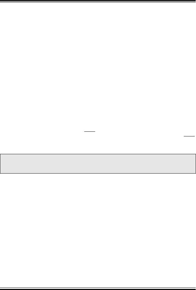
FIGURE 28-1: PIC18F8722 DEVICE FAMILY VOLTAGE-FREQUENCY GRAPH (INDUSTRIAL)
Voltage
6.0V
5.5V
5.0V PIC18F6627/6622/6627/6722
PIC18F8527/8622/8627/8722
4.5V
4.2V
4.0V
3.5V
3.0V
2.5V
2.0V
FMAX
Frequency
FMAX = 20 MHz in 8-bit External Memory mode.
FMAX = 40 MHz in all other modes.
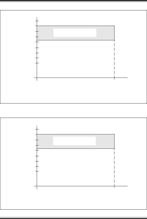
FIGURE 28-2: PIC18F8722 DEVICE FAMILY VOLTAGE-FREQUENCY GRAPH (EXTENDED)
Voltage
6.0V
5.5V
5.0V PIC18F6627/6622/6627/6722
PIC18F8527/8622/8627/8722
4.5V
4.2V
4.0V
3.5V
3.0V
2.5V
2.0V
FMAX
Frequency
FMAX = 20 MHz in 8-bit External Memory mode.
FMAX = 25 MHz in all other modes.
DS39646B-page 378 |
Preliminary |
2004 Microchip Technology Inc. |
PIC18F8722 FAMILY
FIGURE 28-3: PIC18LF8722 DEVICE FAMILY VOLTAGE-FREQUENCY GRAPH (INDUSTRIAL)
|
6.0V |
|
|
|
5.5V |
|
|
|
5.0V |
PIC18LF6627/6622/6627/6722 |
|
|
PIC18LF8527/8622/8627/8722 |
|
|
|
4.5V |
|
|
Voltage |
|
4.2V |
|
4.0V |
|
||
|
|
||
3.5V |
|
|
|
|
|
|
|
|
3.0V |
|
|
|
2.5V |
|
|
|
2.0V |
|
|
|
|
4 MHz |
FMAX |
|
|
Frequency |
|
|
|
In 8-bit External Memory mode: |
|
|
|
FMAX = (9.55 MHz/V) (VDDAPPMIN – 2.0V) + 4 MHz, if VDDAPPMIN ≤ 4.2V; |
|
|
|
FMAX = 25 MHz, if VDDAPPMIN > 4.2V. |
|
In all other modes:
FMAX = (16.36 MHz/V) (VDDAPPMIN – 2.0V) + 4 MHz;
FMAX = 40 MHz, if VDDAPPMIN > 4.2V.
Note: VDDAPPMIN is the minimum voltage of the PICmicro® device in the application.
2004 Microchip Technology Inc.
Preliminary
DS39646B-page 379

PIC18F8722 FAMILY
28.1DC Characteristics: Supply Voltage
PIC18F6X27/6X22/8X27/8X22 (Industrial, Extended)
PIC18LF6X27/6X22/8X27/8X22 (Industrial)
PIC18LF6X27/6X22/8X27/8X22 |
Standard Operating Conditions (unless otherwise stated) |
||||||||
(Industrial) |
|
Operating temperature |
|
-40°C ≤ TA ≤ +85°C for industrial |
|||||
|
|
|
|
|
|
|
|
||
PIC18F6X27/6X22/8X27/8X22 |
Standard Operating Conditions (unless otherwise stated) |
||||||||
Operating temperature |
|
-40°C ≤ TA ≤ +85°C for industrial |
|||||||
(Industrial, Extended) |
|
||||||||
|
|
|
|
|
-40°C ≤ TA ≤ +125°C for extended |
||||
|
|
|
|
|
|
|
|
||
|
|
|
|
|
|
|
|
|
|
Param |
Symbol |
Characteristic |
Min |
Typ |
Max |
Units |
Conditions |
||
No. |
|||||||||
|
|
|
|
|
|
|
|
||
|
|
|
|
|
|
|
|
|
|
|
|
|
|
|
|
|
|
|
|
D001 |
VDD |
Supply Voltage |
|
|
|
|
|
|
|
|
|
|
|
|
|
|
|
|
|
|
|
PIC18LF6X27/6X22/8X27/8X22 |
2.0 |
— |
5.5 |
|
V |
|
|
|
|
|
|
|
|
|
|
|
|
|
|
PIC18F6X27/6X22/8X27/8X22 |
4.2 |
— |
5.5 |
|
V |
|
|
D002 |
VDR |
RAM Data Retention |
1.5 |
— |
— |
|
V |
|
|
|
|
Voltage(1) |
|
|
|
|
|
|
|
D003 |
VPOR |
VDD Start Voltage |
— |
— |
0.7 |
|
V |
See Section 4.3 “Power-on Reset (POR)” for |
|
|
|
to ensure internal |
|
|
|
|
|
details |
|
|
|
Power-on Reset signal |
|
|
|
|
|
|
|
|
|
|
|
|
|
|
|
||
D004 |
SVDD |
VDD Rise Rate |
0.05 |
— |
— |
V/ms |
See Section 4.3 “Power-on Reset (POR)” for |
||
|
|
to ensure internal |
|
|
|
|
|
details |
|
|
|
Power-on Reset signal |
|
|
|
|
|
|
|
|
|
|
|
|
|
|
|
|
|
D005 |
VBOR |
Brown-out Reset Voltage |
|
|
|
|
|
|
|
|
|
|
|
|
|
|
|
|
|
|
|
BORV1:BORV0 = 11 |
2.00 |
2.05 |
2.16 |
|
V |
PIC18LF6627/6722/8627/8722 |
|
|
|
|
|
|
|
|
|
|
|
|
|
BORV1:BORV0 = 11 |
2.00 |
2.11 |
2.22 |
|
V |
PIC18LF6527/6622/8527/8622 |
|
|
|
|
|
|
|
|
|
|
|
|
|
BORV1:BORV0 = 10 |
2.65 |
2.79 |
2.93 |
|
V |
PIC18LF6X27/6X22/8X27/8X22 |
|
|
|
|
|
|
|
|
|
|
|
|
|
BORV1:BORV0 = 01 |
4.11 |
4.33 |
4.55 |
|
V |
All devices |
|
|
|
|
|
|
|
|
|
|
|
|
|
BORV1:BORV0 = 00 |
4.36 |
4.59 |
4.82 |
|
V |
All devices |
|
|
|
|
|
|
|
|
|
|
|
Legend: |
Shading of rows is to assist in readability of the table. |
|
|
|
|
||||
Note 1: |
This is the limit to which VDD can be lowered in Sleep mode, or during a device Reset, without losing RAM data. |
||||||||
DS39646B-page 380 |
Preliminary |
2004 Microchip Technology Inc. |

PIC18F8722 FAMILY
28.2DC Characteristics: Power-Down and Supply Current
PIC18F6X27/6X22/8X27/8X22 (Industrial, Extended)
PIC18LF6X27/6X22/8X27/8X22 (Industrial)
PIC18LF6X27/6X22/8X27/8X22 |
Standard Operating Conditions (unless otherwise stated) |
|
|||||
(Industrial) |
Operating temperature |
-40°C ≤ TA ≤ +85°C for industrial |
|
||||
|
|
|
|
|
|
|
|
PIC18F6X27/6X22/8X27/8X22 |
Standard Operating Conditions (unless otherwise stated) |
|
|||||
Operating temperature |
-40°C ≤ TA ≤ +85°C for industrial |
|
|||||
(Industrial, Extended) |
|
||||||
|
|
|
-40°C ≤ TA ≤ +125°C for extended |
|
|||
|
|
|
|
|
|
||
Param |
Device |
Typ |
Max |
Units |
Conditions |
|
|
No. |
|
||||||
|
|
|
|
|
|
|
|
|
|
|
|
|
|
|
|
|
|
|
|
|
|
|
|
|
Power-Down Current (IPD)(1) |
|
|
|
|
|
|
|
PIC18LF6X27/6X22/8X27/8X22 |
0.12 |
1.2 |
A |
-40°C |
|
VDD = 2.0V, |
|
|
|
|
|
|
|
|
|
|
0.12 |
1.2 |
A |
+25°C |
|
|
|
|
|
(Sleep mode) |
||||
|
|
|
|
|
|
|
|
|
|
0.24 |
6.0 |
A |
+85°C |
|
|
|
|
|
|
||||
|
|
|
|
|
|
|
|
|
PIC18LF6X27/6X22/8X27/8X22 |
0.12 |
1.7 |
A |
-40°C |
|
VDD = 3.0V, |
|
|
|
|
|
|
|
|
|
|
0.12 |
2.4 |
A |
+25°C |
|
|
|
|
|
(Sleep mode) |
||||
|
|
|
|
|
|
|
|
|
|
0.36 |
9.6 |
A |
+85°C |
|
|
|
|
|
|
||||
|
|
|
|
|
|
|
|
|
All devices |
0.12 |
2.4 |
A |
-40°C |
|
|
|
|
|
|
|
|
|
|
|
|
0.12 |
2.5 |
A |
+25°C |
|
VDD = 5.0V, |
|
|
0.48 |
18.0 |
A |
+85°C |
|
(Sleep mode) |
|
|
|
|
|
|
|
|
|
Extended devices only |
12 |
150 |
A |
+125°C |
|
|
|
|
|
|
|
|
|
|
Legend: Shading of rows is to assist in readability of the table.
Note 1: The power-down current in Sleep mode does not depend on the oscillator type. Power-down current is measured with the part in Sleep mode, with all I/O pins in high-impedance state and tied to VDD or VSS and all features that add delta current disabled (such as WDT, Timer1 Oscillator, BOR, etc.).
2:The supply current is mainly a function of operating voltage, frequency and mode. Other factors, such as I/O pin loading and switching rate, oscillator type and circuit, internal code execution pattern and temperature, also have an impact on the current consumption.
The test conditions for all IDD measurements in active operation mode are:
OSC1 = external square wave, from rail-to-rail; all I/O pins tri-stated, pulled to VDD OR VSS; MCLR = VDD; WDT enabled/disabled as specified.
3:Low-power Timer1 oscillator selected.
4:BOR and HLVD enable internal band gap reference. With both modules enabled, current consumption will be less than the sum of both specifications.
2004 Microchip Technology Inc.
Preliminary
DS39646B-page 381

PIC18F8722 FAMILY
28.2DC Characteristics: Power-Down and Supply Current
PIC18F6X27/6X22/8X27/8X22 (Industrial, Extended)
PIC18LF6X27/6X22/8X27/8X22 (Industrial) (Continued)
PIC18LF6X27/6X22/8X27/8X22 |
Standard Operating Conditions (unless otherwise stated) |
|
||||||
(Industrial) |
Operating temperature |
-40°C ≤ TA ≤ +85°C for industrial |
|
|||||
|
|
|
|
|
|
|
|
|
PIC18F6X27/6X22/8X27/8X22 |
Standard Operating Conditions (unless otherwise stated) |
|
||||||
Operating temperature |
-40°C ≤ TA ≤ +85°C for industrial |
|
||||||
(Industrial, Extended) |
|
|||||||
|
|
|
-40°C ≤ TA ≤ +125°C for extended |
|
||||
|
|
|
|
|
|
|||
Param |
Device |
Typ |
Max |
Units |
|
Conditions |
|
|
No. |
|
|
||||||
|
|
|
|
|
|
|
|
|
|
|
|
|
|
|
|
|
|
|
|
|
|
|
|
|
|
|
|
Supply Current (IDD)(2) |
|
|
|
|
|
|
|
|
PIC18LF6X27/6X22/8X27/8X22 |
18 |
39 |
A |
-40°C |
|
|
|
|
|
|
|
|
|
|
|
|
|
|
18 |
36 |
A |
+25°C |
VDD = 2.0V |
|
|
|
|
|
|
|
|
|
|
|
|
|
18 |
42 |
A |
+85°C |
|
|
|
|
|
|
|
|
|
|
|
|
|
PIC18LF6X27/6X22/8X27/8X22 |
48 |
75 |
A |
-40°C |
|
|
|
|
|
|
|
|
|
|
|
FOSC = 31 kHz |
|
|
42 |
72 |
A |
+25°C |
VDD = 3.0V |
|
|
|
|
|
(RC_RUN mode, |
|||||
|
|
|
|
|
|
|
|
|
|
|
36 |
69 |
A |
+85°C |
|
|
|
|
|
|
Internal oscillator source) |
|||||
|
|
|
|
|
|
|
||
|
All devices |
126 |
202 |
A |
-40°C |
|
|
|
|
|
|
|
|
|
|
|
|
|
|
108 |
192 |
A |
+25°C |
VDD = 5.0V |
|
|
|
|
|
|
|
|
|
|
|
|
|
96 |
182 |
A |
+85°C |
|
|
|
|
|
|
|
|
||||
|
|
|
|
|
|
|
|
|
|
Extended devices only |
96 |
300 |
A |
+125°C |
|
|
|
|
|
|
|
|
|
|
|
|
|
PIC18LF6X27/6X22/8X27/8X22 |
0.38 |
1.2 |
mA |
-40°C |
|
|
|
|
|
|
|
|
|
|
|
|
|
|
0.38 |
1.2 |
mA |
+25°C |
VDD = 2.0V |
|
|
|
|
|
|
|
|
|
|
|
|
|
0.38 |
1.2 |
mA |
+85°C |
|
|
|
|
|
|
|
|
|
|
|
|
|
PIC18LF6X27/6X22/8X27/8X22 |
0.72 |
1.6 |
mA |
-40°C |
|
|
|
|
|
|
|
|
|
VDD = 3.0V |
|
FOSC = 1 MHz |
|
|
0.7 |
1.5 |
mA |
+25°C |
|
||
|
|
|
(RC_RUN mode, |
|||||
|
|
|
|
|
|
|
|
|
|
|
0.72 |
1.4 |
mA |
+85°C |
|
|
|
|
|
|
Internal oscillator source) |
|||||
|
|
|
|
|
|
|
||
|
All devices |
1.3 |
2.8 |
mA |
-40°C |
|
|
|
|
|
|
|
|
|
|
|
|
|
|
1.3 |
2.8 |
mA |
+25°C |
VDD = 5.0V |
|
|
|
|
|
|
|
|
|
|
|
|
|
1.2 |
2.7 |
mA |
+85°C |
|
|
|
|
|
|
|
|
||||
|
|
|
|
|
|
|
|
|
|
Extended devices only |
1.2 |
4.0 |
mA |
+125°C |
|
|
|
|
|
|
|
|
|
|
|
|
Legend: Shading of rows is to assist in readability of the table.
Note 1: The power-down current in Sleep mode does not depend on the oscillator type. Power-down current is measured with the part in Sleep mode, with all I/O pins in high-impedance state and tied to VDD or VSS and all features that add delta current disabled (such as WDT, Timer1 Oscillator, BOR, etc.).
2:The supply current is mainly a function of operating voltage, frequency and mode. Other factors, such as I/O pin loading and switching rate, oscillator type and circuit, internal code execution pattern and temperature, also have an impact on the current consumption.
The test conditions for all IDD measurements in active operation mode are:
OSC1 = external square wave, from rail-to-rail; all I/O pins tri-stated, pulled to VDD OR VSS; MCLR = VDD; WDT enabled/disabled as specified.
3:Low-power Timer1 oscillator selected.
4:BOR and HLVD enable internal band gap reference. With both modules enabled, current consumption will be less than the sum of both specifications.
DS39646B-page 382 |
Preliminary |
2004 Microchip Technology Inc. |

PIC18F8722 FAMILY
28.2DC Characteristics: Power-Down and Supply Current
PIC18F6X27/6X22/8X27/8X22 (Industrial, Extended)
PIC18LF6X27/6X22/8X27/8X22 (Industrial) (Continued)
PIC18LF6X27/6X22/8X27/8X22 |
Standard Operating Conditions (unless otherwise stated) |
|
||||||
(Industrial) |
Operating temperature |
-40°C ≤ TA ≤ +85°C for industrial |
|
|||||
|
|
|
|
|
|
|
|
|
PIC18F6X27/6X22/8X27/8X22 |
Standard Operating Conditions (unless otherwise stated) |
|
||||||
Operating temperature |
-40°C ≤ TA ≤ +85°C for industrial |
|
||||||
(Industrial, Extended) |
|
|||||||
|
|
|
-40°C ≤ TA ≤ +125°C for extended |
|
||||
|
|
|
|
|
|
|||
Param |
Device |
Typ |
Max |
Units |
|
Conditions |
|
|
No. |
|
|
||||||
|
|
|
|
|
|
|
|
|
|
|
|
|
|
|
|
|
|
|
|
|
|
|
|
|
|
|
|
Supply Current (IDD)(2) |
|
|
|
|
|
|
|
|
PIC18LF6X27/6X22/8X27/8X22 |
1.0 |
2.5 |
mA |
-40°C |
|
|
|
|
|
|
|
|
|
VDD = 2.0V |
|
|
|
|
1.0 |
2.4 |
mA |
+25°C |
|
|
|
|
|
|
|
|
|
|
|
|
|
|
1.0 |
2.3 |
mA |
+85°C |
|
|
|
|
|
|
|
|
|
|
|
|
|
PIC18LF6X27/6X22/8X27/8X22 |
1.6 |
3.6 |
mA |
-40°C |
|
|
|
|
|
|
|
|
|
VDD = 3.0V |
|
FOSC = 4 MHz |
|
|
1.6 |
3.6 |
mA |
+25°C |
|
||
|
|
|
(RC_RUN mode, |
|||||
|
|
|
|
|
|
|
|
|
|
|
1.6 |
3.6 |
mA |
+85°C |
|
|
|
|
|
|
Internal oscillator source) |
|||||
|
|
|
|
|
|
|
||
|
All devices |
3.0 |
6.3 |
mA |
-40°C |
|
|
|
|
|
|
|
|
|
|
|
|
|
|
3.0 |
6.0 |
mA |
+25°C |
VDD = 5.0V |
|
|
|
|
|
|
|
|
|
|
|
|
|
3.0 |
5.8 |
mA |
+85°C |
|
|
|
|
|
|
|
|
||||
|
|
|
|
|
|
|
|
|
|
Extended devices only |
3.0 |
12 |
mA |
+125°C |
|
|
|
|
|
|
|
|
|
|
|
|
|
PIC18LF6X27/6X22/8X27/8X22 |
3.5 |
9.6 |
A |
-40°C |
|
|
|
|
|
|
|
|
|
|
|
|
|
|
3.7 |
9.6 |
A |
+25°C |
VDD = 2.0V |
|
|
|
|
|
|
|
|
|
|
|
|
|
4.3 |
32 |
A |
+85°C |
|
|
|
|
|
|
|
|
|
|
|
|
|
PIC18LF6X27/6X22/8X27/8X22 |
5.4 |
13 |
A |
-40°C |
|
|
|
|
|
|
|
|
|
|
|
FOSC = 31 kHz |
|
|
5.7 |
13 |
A |
+25°C |
VDD = 3.0V |
|
|
|
|
|
(RC_IDLE mode, |
|||||
|
|
|
|
|
|
|
|
|
|
|
7.0 |
38 |
A |
+85°C |
|
|
|
|
|
|
Internal oscillator source) |
|||||
|
|
|
|
|
|
|
||
|
All devices |
11 |
19 |
A |
-40°C |
|
|
|
|
|
|
|
|
|
|
|
|
|
|
11.8 |
19 |
A |
+25°C |
VDD = 5.0V |
|
|
|
|
|
|
|
|
|
|
|
|
|
13.5 |
43 |
A |
+85°C |
|
|
|
|
|
|
|
|
||||
|
|
|
|
|
|
|
|
|
|
Extended devices only |
25 |
216 |
A |
+125°C |
|
|
|
|
|
|
|
|
|
|
|
|
Legend: |
Shading of rows is to assist in readability of the table. |
|
|
|
|
|||
Note 1: |
The power-down current in Sleep mode does not depend on the oscillator type. Power-down current is measured with |
|||||||
|
the part in Sleep mode, with all I/O pins in high-impedance state and tied to VDD or VSS and all features that add delta |
|||||||
|
current disabled (such as WDT, Timer1 Oscillator, BOR, etc.). |
|
|
|
||||
2:The supply current is mainly a function of operating voltage, frequency and mode. Other factors, such as I/O pin loading and switching rate, oscillator type and circuit, internal code execution pattern and temperature, also have an impact on the current consumption.
The test conditions for all IDD measurements in active operation mode are:
OSC1 = external square wave, from rail-to-rail; all I/O pins tri-stated, pulled to VDD OR VSS; MCLR = VDD; WDT enabled/disabled as specified.
3:Low-power Timer1 oscillator selected.
4:BOR and HLVD enable internal band gap reference. With both modules enabled, current consumption will be less than the sum of both specifications.
2004 Microchip Technology Inc.
Preliminary
DS39646B-page 383

PIC18F8722 FAMILY
28.2DC Characteristics: Power-Down and Supply Current
PIC18F6X27/6X22/8X27/8X22 (Industrial, Extended)
PIC18LF6X27/6X22/8X27/8X22 (Industrial) (Continued)
PIC18LF6X27/6X22/8X27/8X22 |
Standard Operating Conditions (unless otherwise stated) |
|
||||||
(Industrial) |
Operating temperature |
-40°C ≤ TA ≤ +85°C for industrial |
|
|||||
|
|
|
|
|
|
|
|
|
PIC18F6X27/6X22/8X27/8X22 |
Standard Operating Conditions (unless otherwise stated) |
|
||||||
Operating temperature |
-40°C ≤ TA ≤ +85°C for industrial |
|
||||||
(Industrial, Extended) |
|
|||||||
|
|
|
-40°C ≤ TA ≤ +125°C for extended |
|
||||
|
|
|
|
|
|
|||
Param |
Device |
Typ |
Max |
Units |
|
Conditions |
|
|
No. |
|
|
||||||
|
|
|
|
|
|
|
|
|
|
|
|
|
|
|
|
|
|
|
|
|
|
|
|
|
|
|
|
Supply Current (IDD)(2) |
|
|
|
|
|
|
|
|
PIC18LF6X27/6X22/8X27/8X22 |
200 |
420 |
A |
-40°C |
|
|
|
|
|
|
|
|
|
|
|
|
|
|
210 |
420 |
A |
+25°C |
VDD = 2.0V |
|
|
|
|
|
|
|
|
|
|
|
|
|
228 |
420 |
A |
+85°C |
|
|
|
|
|
|
|
|
|
|
|
|
|
PIC18LF6X27/6X22/8X27/8X22 |
300 |
600 |
A |
-40°C |
|
|
|
|
|
|
|
|
|
|
|
FOSC = 1 MHz |
|
|
324 |
600 |
A |
+25°C |
VDD = 3.0V |
|
|
|
|
|
(RC_IDLE mode, |
|||||
|
|
|
|
|
|
|
|
|
|
|
350 |
600 |
A |
+85°C |
|
|
|
|
|
|
Internal oscillator source) |
|||||
|
|
|
|
|
|
|
||
|
All devices |
0.6 |
1.2 |
mA |
-40°C |
|
|
|
|
|
|
|
|
|
|
|
|
|
|
0.62 |
1.2 |
mA |
+25°C |
VDD = 5.0V |
|
|
|
|
|
|
|
|
|
|
|
|
|
0.67 |
1.2 |
mA |
+85°C |
|
|
|
|
|
|
|
|
||||
|
|
|
|
|
|
|
|
|
|
Extended devices only |
0.72 |
3.5 |
mA |
+125°C |
|
|
|
|
|
|
|
|
|
|
|
|
|
PIC18LF6X27/6X22/8X27/8X22 |
410 |
600 |
A |
-40°C |
|
|
|
|
|
|
|
|
|
|
|
|
|
|
420 |
600 |
A |
+25°C |
VDD = 2.0V |
|
|
|
|
|
|
|
|
|
|
|
|
|
430 |
600 |
A |
+85°C |
|
|
|
|
|
|
|
|
|
|
|
|
|
PIC18LF6X27/6X22/8X27/8X22 |
0.63 |
1.1 |
mA |
-40°C |
|
|
|
|
|
|
|
|
|
VDD = 3.0V |
|
FOSC = 4 MHz |
|
|
0.65 |
1.1 |
mA |
+25°C |
|
||
|
|
|
(RC_IDLE mode, |
|||||
|
|
|
|
|
|
|
|
|
|
|
0.69 |
1.1 |
mA |
+85°C |
|
|
|
|
|
|
Internal oscillator source) |
|||||
|
|
|
|
|
|
|
||
|
All devices |
1.2 |
1.9 |
mA |
-40°C |
|
|
|
|
|
|
|
|
|
|
|
|
|
|
1.3 |
1.8 |
mA |
+25°C |
VDD = 5.0V |
|
|
|
|
|
|
|
|
|
|
|
|
|
1.2 |
1.7 |
mA |
+85°C |
|
|
|
|
|
|
|
|
||||
|
|
|
|
|
|
|
|
|
|
Extended devices only |
1.2 |
6.0 |
mA |
+125°C |
|
|
|
|
|
|
|
|
|
|
|
|
Legend: |
Shading of rows is to assist in readability of the table. |
|
|
|
|
|||
Note 1: |
The power-down current in Sleep mode does not depend on the oscillator type. Power-down current is measured with |
|||||||
|
the part in Sleep mode, with all I/O pins in high-impedance state and tied to VDD or VSS and all features that add delta |
|||||||
|
current disabled (such as WDT, Timer1 Oscillator, BOR, etc.). |
|
|
|
||||
2:The supply current is mainly a function of operating voltage, frequency and mode. Other factors, such as I/O pin loading and switching rate, oscillator type and circuit, internal code execution pattern and temperature, also have an impact on the current consumption.
The test conditions for all IDD measurements in active operation mode are:
OSC1 = external square wave, from rail-to-rail; all I/O pins tri-stated, pulled to VDD OR VSS; MCLR = VDD; WDT enabled/disabled as specified.
3:Low-power Timer1 oscillator selected.
4:BOR and HLVD enable internal band gap reference. With both modules enabled, current consumption will be less than the sum of both specifications.
DS39646B-page 384 |
Preliminary |
2004 Microchip Technology Inc. |

PIC18F8722 FAMILY
28.2DC Characteristics: Power-Down and Supply Current
PIC18F6X27/6X22/8X27/8X22 (Industrial, Extended)
PIC18LF6X27/6X22/8X27/8X22 (Industrial) (Continued)
PIC18LF6X27/6X22/8X27/8X22 |
Standard Operating Conditions (unless otherwise stated) |
|
||||||
(Industrial) |
Operating temperature |
-40°C ≤ TA ≤ +85°C for industrial |
|
|||||
|
|
|
|
|
|
|
|
|
PIC18F6X27/6X22/8X27/8X22 |
Standard Operating Conditions (unless otherwise stated) |
|
||||||
Operating temperature |
-40°C ≤ TA ≤ +85°C for industrial |
|
||||||
(Industrial, Extended) |
|
|||||||
|
|
|
-40°C ≤ TA ≤ +125°C for extended |
|
||||
|
|
|
|
|
|
|||
Param |
Device |
Typ |
Max |
Units |
|
Conditions |
|
|
No. |
|
|
||||||
|
|
|
|
|
|
|
|
|
|
|
|
|
|
|
|
|
|
|
|
|
|
|
|
|
|
|
|
Supply Current (IDD)(2) |
|
|
|
|
|
|
|
|
PIC18LF6X27/6X22/8X27/8X22 |
300 |
600 |
A |
-40°C |
|
|
|
|
|
|
|
|
|
|
|
|
|
|
310 |
600 |
A |
+25°C |
VDD = 2.0V |
|
|
|
|
|
|
|
|
|
|
|
|
|
300 |
600 |
A |
+85°C |
|
|
|
|
|
|
|
|
|
|
|
|
|
PIC18LF6X27/6X22/8X27/8X22 |
660 |
855 |
A |
-40°C |
|
|
|
|
|
|
|
|
|
|
|
FOSC = 1 MHZ |
|
|
580 |
780 |
A |
+25°C |
VDD = 3.0V |
|
|
|
|
|
(PRI_RUN mode, |
|||||
|
|
|
|
|
|
|
|
|
|
|
550 |
780 |
A |
+85°C |
|
|
|
|
|
|
|
EC oscillator) |
||||
|
|
|
|
|
|
|
|
|
|
All devices |
1.5 |
1.9 |
mA |
-40°C |
|
|
|
|
|
|
|
|
|
|
|
|
|
|
1.4 |
1.8 |
mA |
+25°C |
VDD = 5.0V |
|
|
|
|
|
|
|
|
|
|
|
|
|
1.3 |
1.7 |
mA |
+85°C |
|
|
|
|
|
|
|
|
||||
|
|
|
|
|
|
|
|
|
|
Extended devices only |
1.3 |
4.2 |
mA |
+125°C |
|
|
|
|
|
|
|
|
|
|
|
|
|
PIC18LF6X27/6X22/8X27/8X22 |
0.86 |
2.4 |
mA |
-40°C |
|
|
|
|
|
|
|
|
|
|
|
|
|
|
0.88 |
2.4 |
mA |
+25°C |
VDD = 2.0V |
|
|
|
|
|
|
|
|
|
|
|
|
|
0.88 |
2.4 |
mA |
+85°C |
|
|
|
|
|
|
|
|
|
|
|
|
|
PIC18LF6X27/6X22/8X27/8X22 |
1.6 |
3.6 |
mA |
-40°C |
|
|
|
|
|
|
|
|
|
VDD = 3.0V |
|
FOSC = 4 MHz |
|
|
1.6 |
3.6 |
mA |
+25°C |
|
||
|
|
|
(PRI_RUN mode, |
|||||
|
|
|
|
|
|
|
|
|
|
|
1.6 |
3.6 |
mA |
+85°C |
|
|
|
|
|
|
|
EC oscillator) |
||||
|
|
|
|
|
|
|
|
|
|
All devices |
3.2 |
7.2 |
mA |
-40°C |
|
|
|
|
|
|
|
|
|
|
|
|
|
|
3.1 |
7.2 |
mA |
+25°C |
VDD = 5.0V |
|
|
|
|
|
|
|
|
|
|
|
|
|
3.0 |
7.2 |
mA |
+85°C |
|
|
|
|
|
|
|
|
||||
|
|
|
|
|
|
|
|
|
|
Extended devices only |
3.1 |
8.4 |
mA |
+125°C |
|
|
|
|
|
|
|
|
|
|
|
|
Legend: |
Shading of rows is to assist in readability of the table. |
|
|
|
|
|||
Note 1: |
The power-down current in Sleep mode does not depend on the oscillator type. Power-down current is measured with |
|||||||
|
the part in Sleep mode, with all I/O pins in high-impedance state and tied to VDD or VSS and all features that add delta |
|||||||
|
current disabled (such as WDT, Timer1 Oscillator, BOR, etc.). |
|
|
|
||||
2:The supply current is mainly a function of operating voltage, frequency and mode. Other factors, such as I/O pin loading and switching rate, oscillator type and circuit, internal code execution pattern and temperature, also have an impact on the current consumption.
The test conditions for all IDD measurements in active operation mode are:
OSC1 = external square wave, from rail-to-rail; all I/O pins tri-stated, pulled to VDD OR VSS; MCLR = VDD; WDT enabled/disabled as specified.
3:Low-power Timer1 oscillator selected.
4:BOR and HLVD enable internal band gap reference. With both modules enabled, current consumption will be less than the sum of both specifications.
2004 Microchip Technology Inc.
Preliminary
DS39646B-page 385

PIC18F8722 FAMILY
28.2DC Characteristics: Power-Down and Supply Current
PIC18F6X27/6X22/8X27/8X22 (Industrial, Extended)
PIC18LF6X27/6X22/8X27/8X22 (Industrial) (Continued)
PIC18LF6X27/6X22/8X27/8X22 |
Standard Operating Conditions (unless otherwise stated) |
|
||||||
(Industrial) |
Operating temperature |
-40°C ≤ TA ≤ +85°C for industrial |
|
|||||
|
|
|
|
|
|
|
|
|
PIC18F6X27/6X22/8X27/8X22 |
Standard Operating Conditions (unless otherwise stated) |
|
||||||
Operating temperature |
-40°C ≤ TA ≤ +85°C for industrial |
|
||||||
(Industrial, Extended) |
|
|||||||
|
|
|
-40°C ≤ TA ≤ +125°C for extended |
|
||||
|
|
|
|
|
|
|||
Param |
Device |
Typ |
Max |
Units |
|
Conditions |
|
|
No. |
|
|
||||||
|
|
|
|
|
|
|
|
|
|
|
|
|
|
|
|
|
|
|
|
|
|
|
|
|
|
|
|
Supply Current (IDD)(2) |
|
|
|
|
|
|
|
|
Extended devices only |
10 |
25 |
mA |
+125°C |
VDD = 4.2V |
|
FOSC = 25 MHz |
|
|
|
|
|
|
|
|
(PRI_RUN mode, |
|
|
13 |
33 |
mA |
+125°C |
VDD = 5.0V |
|
|
|
|
|
EC oscillator) |
|||||
|
|
|
|
|
|
|
||
|
|
|
|
|
|
|
|
|
|
|
|
|
|
|
|
|
|
|
All devices |
18 |
42 |
mA |
-40°C |
|
|
|
|
|
|
|
|
|
|
|
|
|
|
19 |
42 |
mA |
+25°C |
VDD = 4.2V |
|
|
|
|
|
|
|
|
|
|
FOSC = 40 MHZ |
|
|
19 |
42 |
mA |
+85°C |
|
|
|
|
|
|
|
(PRI_RUN mode, |
||||
|
|
|
|
|
|
|
|
|
|
All devices |
25 |
48 |
mA |
-40°C |
|
|
|
|
|
|
EC oscillator) |
|||||
|
|
|
|
|
|
VDD = 5.0V |
|
|
|
|
25 |
48 |
mA |
+25°C |
|
|
|
|
|
|
|
|
|
|
|
|
|
|
25 |
48 |
mA |
+85°C |
|
|
|
|
|
|
|
|
|
|
|
|
Legend: |
Shading of rows is to assist in readability of the table. |
|
|
|
|
|||
Note 1: |
The power-down current in Sleep mode does not depend on the oscillator type. Power-down current is measured with |
|||||||
|
the part in Sleep mode, with all I/O pins in high-impedance state and tied to VDD or VSS and all features that add delta |
|||||||
|
current disabled (such as WDT, Timer1 Oscillator, BOR, etc.). |
|
|
|
||||
2:The supply current is mainly a function of operating voltage, frequency and mode. Other factors, such as I/O pin loading and switching rate, oscillator type and circuit, internal code execution pattern and temperature, also have an impact on the current consumption.
The test conditions for all IDD measurements in active operation mode are:
OSC1 = external square wave, from rail-to-rail; all I/O pins tri-stated, pulled to VDD OR VSS; MCLR = VDD; WDT enabled/disabled as specified.
3:Low-power Timer1 oscillator selected.
4:BOR and HLVD enable internal band gap reference. With both modules enabled, current consumption will be less than the sum of both specifications.
DS39646B-page 386 |
Preliminary |
2004 Microchip Technology Inc. |

PIC18F8722 FAMILY
28.2DC Characteristics: Power-Down and Supply Current
PIC18F6X27/6X22/8X27/8X22 (Industrial, Extended)
PIC18LF6X27/6X22/8X27/8X22 (Industrial) (Continued)
PIC18LF6X27/6X22/8X27/8X22 |
Standard Operating Conditions (unless otherwise stated) |
|
||||||
(Industrial) |
Operating temperature |
-40°C ≤ TA ≤ +85°C for industrial |
|
|||||
|
|
|
|
|
|
|
|
|
PIC18F6X27/6X22/8X27/8X22 |
Standard Operating Conditions (unless otherwise stated) |
|
||||||
Operating temperature |
-40°C ≤ TA ≤ +85°C for industrial |
|
||||||
(Industrial, Extended) |
|
|||||||
|
|
|
-40°C ≤ TA ≤ +125°C for extended |
|||||
|
|
|
|
|
||||
Param |
Device |
Typ |
Max |
Units |
|
Conditions |
|
|
No. |
|
|
||||||
|
|
|
|
|
|
|
|
|
|
|
|
|
|
|
|
|
|
|
|
|
|
|
|
|
|
|
|
Supply Current (IDD)(2) |
|
|
|
|
|
|
|
|
All devices |
9.0 |
19 |
mA |
-40°C |
|
|
|
|
|
|
|
|
|
|
|
FOSC = 4 MHZ. |
|
|
9.0 |
18 |
mA |
+25°C |
VDD = 4.2V |
|
|
|
|
|
16 MHz internal |
|||||
|
|
|
|
|
|
|
||
|
|
9.0 |
17 |
mA |
+85°C |
|
||
|
|
|
|
(PRI_RUN HS+PLL) |
||||
|
|
|
|
|
|
|
|
|
|
Extended devices only |
9.6 |
30 |
mA |
+125°C |
|
|
|
|
|
|
|
|
|
|
|
|
|
All devices |
12 |
25 |
mA |
-40°C |
|
|
|
|
|
|
|
|
|
|
|
FOSC = 4 MHZ, |
|
|
12 |
24 |
mA |
+25°C |
VDD = 5.0V |
|
|
|
|
|
16 MHz internal |
|||||
|
|
|
|
|
|
|
||
|
|
12 |
23 |
mA |
+85°C |
|
||
|
|
|
|
(PRI_RUN HS+PLL) |
||||
|
|
|
|
|
|
|
|
|
|
Extended devices only |
12 |
42 |
mA |
+125°C |
|
|
|
|
|
|
|
|
|
|
|
|
|
All devices |
20 |
42 |
mA |
-40°C |
|
|
FOSC = 10 MHZ, |
|
|
|
|
|
|
|
|
|
|
|
20 |
42 |
mA |
+25°C |
VDD = 4.2V |
|
40 MHz internal |
|
|
|
|
|
|
|
|
(PRI_RUN HS+PLL) |
|
|
20 |
42 |
mA |
+85°C |
|
|
|
|
|
|
|
|
||||
|
|
|
|
|
|
|
|
|
|
All devices |
28 |
48 |
mA |
-40°C |
|
|
FOSC = 10 MHZ, |
|
|
|
|
|
|
|
|
|
|
|
28 |
48 |
mA |
+25°C |
VDD = 5.0V |
|
40 MHz internal |
|
|
|
|
|
|
|
|
(PRI_RUN HS+PLL) |
|
|
28 |
48 |
mA |
+85°C |
|
|
|
|
|
|
|
|
||||
|
|
|
|
|
|
|
|
|
Legend: Shading of rows is to assist in readability of the table.
Note 1: The power-down current in Sleep mode does not depend on the oscillator type. Power-down current is measured with the part in Sleep mode, with all I/O pins in high-impedance state and tied to VDD or VSS and all features that add delta current disabled (such as WDT, Timer1 Oscillator, BOR, etc.).
2:The supply current is mainly a function of operating voltage, frequency and mode. Other factors, such as I/O pin loading and switching rate, oscillator type and circuit, internal code execution pattern and temperature, also have an impact on the current consumption.
The test conditions for all IDD measurements in active operation mode are:
OSC1 = external square wave, from rail-to-rail; all I/O pins tri-stated, pulled to VDD OR VSS; MCLR = VDD; WDT enabled/disabled as specified.
3:Low-power Timer1 oscillator selected.
4:BOR and HLVD enable internal band gap reference. With both modules enabled, current consumption will be less than the sum of both specifications.
2004 Microchip Technology Inc.
Preliminary
DS39646B-page 387

PIC18F8722 FAMILY
28.2DC Characteristics: Power-Down and Supply Current
PIC18F6X27/6X22/8X27/8X22 (Industrial, Extended)
PIC18LF6X27/6X22/8X27/8X22 (Industrial) (Continued)
PIC18LF6X27/6X22/8X27/8X22 |
Standard Operating Conditions (unless otherwise stated) |
|
||||||
(Industrial) |
Operating temperature |
-40°C ≤ TA ≤ +85°C for industrial |
|
|||||
|
|
|
|
|
|
|
|
|
PIC18F6X27/6X22/8X27/8X22 |
Standard Operating Conditions (unless otherwise stated) |
|
||||||
Operating temperature |
-40°C ≤ TA ≤ +85°C for industrial |
|
||||||
(Industrial, Extended) |
|
|||||||
|
|
|
-40°C ≤ TA ≤ +125°C for extended |
|
||||
|
|
|
|
|
|
|||
Param |
Device |
Typ |
Max |
Units |
|
Conditions |
|
|
No. |
|
|
||||||
|
|
|
|
|
|
|
|
|
|
|
|
|
|
|
|
|
|
|
|
|
|
|
|
|
|
|
|
Supply Current (IDD)(2) |
|
|
|
|
|
|
|
|
PIC18LF6X27/6X22/8X27/8X22 |
78 |
215 |
A |
-40°C |
|
|
|
|
|
|
|
|
|
|
|
|
|
|
78 |
210 |
A |
+25°C |
VDD = 2.0V |
|
|
|
|
|
|
|
|
|
|
|
|
|
84 |
205 |
A |
+85°C |
|
|
|
|
|
|
|
|
|
|
|
|
|
PIC18LF6X27/6X22/8X27/8X22 |
144 |
325 |
A |
-40°C |
|
|
|
|
|
|
|
|
|
|
|
FOSC = 1 MHz |
|
|
144 |
300 |
A |
+25°C |
VDD = 3.0V |
|
|
|
|
|
(PRI_IDLE mode, |
|||||
|
|
|
|
|
|
|
|
|
|
|
144 |
288 |
A |
+85°C |
|
|
|
|
|
|
|
EC oscillator) |
||||
|
|
|
|
|
|
|
|
|
|
All devices |
360 |
575 |
A |
-40°C |
|
|
|
|
|
|
|
|
|
|
|
|
|
|
290 |
540 |
A |
+25°C |
VDD = 5.0V |
|
|
|
|
|
|
|
|
|
|
|
|
|
360 |
515 |
A |
+85°C |
|
|
|
|
|
|
|
|
||||
|
|
|
|
|
|
|
|
|
|
Extended devices only |
0.38 |
1.1 |
mA |
+125°C |
|
|
|
|
|
|
|
|
|
|
|
|
|
PIC18LF6X27/6X22/8X27/8X22 |
312 |
570 |
A |
-40°C |
|
|
|
|
|
|
|
|
|
|
|
|
|
|
305 |
540 |
A |
+25°C |
VDD = 2.0V |
|
|
|
|
|
|
|
|
|
|
|
|
|
324 |
515 |
A |
+85°C |
|
|
|
|
|
|
|
|
|
|
|
|
|
PIC18LF6X27/6X22/8X27/8X22 |
0.5 |
1.1 |
mA |
-40°C |
|
|
|
|
|
|
|
|
|
VDD = 3.0V |
|
FOSC = 4 MHz |
|
|
0.6 |
1.0 |
mA |
+25°C |
|
||
|
|
|
(PRI_IDLE mode, |
|||||
|
|
|
|
|
|
|
|
|
|
|
0.6 |
0.9 |
mA |
+85°C |
|
|
|
|
|
|
|
EC oscillator) |
||||
|
|
|
|
|
|
|
|
|
|
All devices |
1.1 |
1.8 |
mA |
-40°C |
|
|
|
|
|
|
|
|
|
|
|
|
|
|
1.1 |
1.7 |
mA |
+25°C |
VDD = 5.0V |
|
|
|
|
|
|
|
|
|
|
|
|
|
1.1 |
1.6 |
mA |
+85°C |
|
|
|
|
|
|
|
|
||||
|
|
|
|
|
|
|
|
|
|
Extended devices only |
1.2 |
3.1 |
mA |
+125°C |
|
|
|
|
|
|
|
|
|
|
|
|
Legend: |
Shading of rows is to assist in readability of the table. |
|
|
|
|
|||
Note 1: |
The power-down current in Sleep mode does not depend on the oscillator type. Power-down current is measured with |
|||||||
|
the part in Sleep mode, with all I/O pins in high-impedance state and tied to VDD or VSS and all features that add delta |
|||||||
|
current disabled (such as WDT, Timer1 Oscillator, BOR, etc.). |
|
|
|
||||
2:The supply current is mainly a function of operating voltage, frequency and mode. Other factors, such as I/O pin loading and switching rate, oscillator type and circuit, internal code execution pattern and temperature, also have an impact on the current consumption.
The test conditions for all IDD measurements in active operation mode are:
OSC1 = external square wave, from rail-to-rail; all I/O pins tri-stated, pulled to VDD OR VSS; MCLR = VDD; WDT enabled/disabled as specified.
3:Low-power Timer1 oscillator selected.
4:BOR and HLVD enable internal band gap reference. With both modules enabled, current consumption will be less than the sum of both specifications.
DS39646B-page 388 |
Preliminary |
2004 Microchip Technology Inc. |
PIC18F8722 FAMILY
28.2DC Characteristics: Power-Down and Supply Current
PIC18F6X27/6X22/8X27/8X22 (Industrial, Extended)
PIC18LF6X27/6X22/8X27/8X22 (Industrial) (Continued)
PIC18LF6X27/6X22/8X27/8X22 |
Standard Operating Conditions (unless otherwise stated) |
|
||||||
(Industrial) |
Operating temperature |
-40°C ≤ TA ≤ +85°C for industrial |
|
|||||
|
|
|
|
|
|
|
|
|
PIC18F6X27/6X22/8X27/8X22 |
Standard Operating Conditions (unless otherwise stated) |
|
||||||
Operating temperature |
-40°C ≤ TA ≤ +85°C for industrial |
|
||||||
(Industrial, Extended) |
|
|||||||
|
|
|
-40°C ≤ TA ≤ +125°C for extended |
|
||||
|
|
|
|
|
|
|||
Param |
Device |
Typ |
Max |
Units |
|
Conditions |
|
|
No. |
|
|
||||||
|
|
|
|
|
|
|
|
|
|
|
|
|
|
|
|
|
|
|
|
|
|
|
|
|
|
|
|
Supply Current (IDD)(2) |
|
|
|
|
|
|
|
|
Extended devices only |
3.4 |
8.4 |
mA |
+125°C |
VDD = 4.2V |
|
FOSC = 25 MHz |
|
|
|
|
|
|
|
|
(PRI_IDLE mode, |
|
|
5.2 |
13 |
mA |
+125°C |
VDD = 5.0V |
|
|
|
|
|
EC oscillator) |
|||||
|
|
|
|
|
|
|
|
|
|
|
|
|
|
|
|
|
|
|
All devices |
7.2 |
19 |
mA |
-40°C |
|
|
|
|
|
|
|
|
|
|
|
|
|
|
7.4 |
19 |
mA |
+25°C |
VDD = 4.2 V |
|
|
|
|
|
|
|
|
|
|
FOSC = 40 MHz |
|
|
7.8 |
19 |
mA |
+85°C |
|
|
|
|
|
|
|
(PRI_IDLE mode, |
||||
|
|
|
|
|
|
|
|
|
|
All devices |
9.7 |
21 |
mA |
-40°C |
|
|
|
|
|
|
EC oscillator) |
|||||
|
|
|
|
|
|
VDD = 5.0V |
|
|
|
|
11 |
21 |
mA |
+25°C |
|
|
|
|
|
|
|
|
|
|
|
|
|
|
10 |
21 |
mA |
+85°C |
|
|
|
|
|
|
|
|
|
|
|
|
Legend: |
Shading of rows is to assist in readability of the table. |
|
|
|
|
|||
Note 1: |
The power-down current in Sleep mode does not depend on the oscillator type. Power-down current is measured with |
|||||||
|
the part in Sleep mode, with all I/O pins in high-impedance state and tied to VDD or VSS and all features that add delta |
|||||||
|
current disabled (such as WDT, Timer1 Oscillator, BOR, etc.). |
|
|
|
||||
2:The supply current is mainly a function of operating voltage, frequency and mode. Other factors, such as I/O pin loading and switching rate, oscillator type and circuit, internal code execution pattern and temperature, also have an impact on the current consumption.
The test conditions for all IDD measurements in active operation mode are:
OSC1 = external square wave, from rail-to-rail; all I/O pins tri-stated, pulled to VDD OR VSS; MCLR = VDD; WDT enabled/disabled as specified.
3:Low-power Timer1 oscillator selected.
4:BOR and HLVD enable internal band gap reference. With both modules enabled, current consumption will be less than the sum of both specifications.
2004 Microchip Technology Inc.
Preliminary
DS39646B-page 389

PIC18F8722 FAMILY
28.2DC Characteristics: Power-Down and Supply Current
PIC18F6X27/6X22/8X27/8X22 (Industrial, Extended)
PIC18LF6X27/6X22/8X27/8X22 (Industrial) (Continued)
PIC18LF6X27/6X22/8X27/8X22 |
Standard Operating Conditions (unless otherwise stated) |
|
||||||
(Industrial) |
Operating temperature |
-40°C ≤ TA ≤ +85°C for industrial |
|
|||||
|
|
|
|
|
|
|
|
|
PIC18F6X27/6X22/8X27/8X22 |
Standard Operating Conditions (unless otherwise stated) |
|
||||||
Operating temperature |
-40°C ≤ TA ≤ +85°C for industrial |
|
||||||
(Industrial, Extended) |
|
|||||||
|
|
|
-40°C ≤ TA ≤ +125°C for extended |
|||||
|
|
|
|
|
||||
Param |
Device |
Typ |
Max |
Units |
|
Conditions |
|
|
No. |
|
|
||||||
|
|
|
|
|
|
|
|
|
|
|
|
|
|
|
|
|
|
|
|
|
|
|
|
|
|
|
|
Supply Current (IDD)(2) |
|
|
|
|
|
|
|
|
PIC18LF6X27/6X22/8X27/8X22 |
17 |
48 |
A |
-40°C |
|
|
|
|
|
|
|
|
|
|
|
|
|
|
18 |
48 |
A |
+25°C |
VDD = 2.0V |
|
|
|
|
|
|
|
|
|
|
|
|
|
19 |
48 |
A |
+70°C |
|
|
|
|
|
|
|
|
|
|
|
|
|
PIC18LF6X27/6X22/8X27/8X22 |
48 |
89 |
A |
-40°C |
|
|
FOSC = 32 kHz(3) |
|
|
42 |
84 |
A |
+25°C |
VDD = 3.0V |
|
(SEC_RUN mode, |
|
|
|
|
|
|
|
|
Timer1 as clock) |
|
|
37 |
80 |
A |
+70°C |
|
|
|
|
|
|
|
|
||||
|
|
|
|
|
|
|
|
|
|
All devices |
120 |
180 |
A |
-40°C |
|
|
|
|
|
|
|
|
|
|
|
|
|
|
97 |
180 |
A |
+25°C |
VDD = 5.0V |
|
|
|
|
|
|
|
|
|
|
|
|
|
90 |
180 |
A |
+70°C |
|
|
|
|
|
|
|
|
|
|
|
|
|
PIC18LF6X27/6X22/8X27/8X22 |
3.0 |
14 |
A |
-40°C |
|
|
|
|
|
|
|
|
|
|
|
|
|
|
4.4 |
14 |
A |
+25°C |
VDD = 2.0V |
|
|
|
|
|
|
|
|
|
|
|
|
|
5.4 |
14 |
A |
+70°C |
|
|
|
|
|
|
|
|
|
|
|
|
|
PIC18LF6X27/6X22/8X27/8X22 |
6.0 |
18 |
A |
-40°C |
|
|
FOSC = 32 kHz(3) |
|
|
6.5 |
18 |
A |
+25°C |
VDD = 3.0V |
|
(SEC_IDLE mode, |
|
|
|
|
|
|
|
|
Timer1 as clock) |
|
|
7.6 |
18 |
A |
+70°C |
|
|
|
|
|
|
|
|
||||
|
|
|
|
|
|
|
|
|
|
All devices |
10.0 |
30 |
A |
-40°C |
|
|
|
|
|
|
|
|
|
|
|
|
|
|
10.5 |
30 |
A |
+25°C |
VDD = 5.0V |
|
|
|
|
|
|
|
|
|
|
|
|
|
11.0 |
43 |
A |
+70°C |
|
|
|
|
|
|
|
|
|
|
|
|
Legend: |
Shading of rows is to assist in readability of the table. |
Note 1: |
The power-down current in Sleep mode does not depend on the oscillator type. Power-down current is measured with |
|
the part in Sleep mode, with all I/O pins in high-impedance state and tied to VDD or VSS and all features that add delta |
|
current disabled (such as WDT, Timer1 Oscillator, BOR, etc.). |
2:The supply current is mainly a function of operating voltage, frequency and mode. Other factors, such as I/O pin loading and switching rate, oscillator type and circuit, internal code execution pattern and temperature, also have an impact on the current consumption.
The test conditions for all IDD measurements in active operation mode are:
OSC1 = external square wave, from rail-to-rail; all I/O pins tri-stated, pulled to VDD OR VSS; MCLR = VDD; WDT enabled/disabled as specified.
3:Low-power Timer1 oscillator selected.
4:BOR and HLVD enable internal band gap reference. With both modules enabled, current consumption will be less than the sum of both specifications.
DS39646B-page 390 |
Preliminary |
2004 Microchip Technology Inc. |

PIC18F8722 FAMILY
28.2DC Characteristics: Power-Down and Supply Current
PIC18F6X27/6X22/8X27/8X22 (Industrial, Extended)
PIC18LF6X27/6X22/8X27/8X22 (Industrial) (Continued)
PIC18LF6X27/6X22/8X27/8X22 |
Standard Operating Conditions (unless otherwise stated) |
|
||||||
(Industrial) |
Operating temperature |
-40°C ≤ TA ≤ +85°C for industrial |
|
|||||
|
|
|
|
|
|
|
|
|
PIC18F6X27/6X22/8X27/8X22 |
Standard Operating Conditions (unless otherwise stated) |
|
||||||
Operating temperature |
-40°C ≤ TA ≤ +85°C for industrial |
|
||||||
(Industrial, Extended) |
|
|||||||
|
|
|
-40°C ≤ TA ≤ +125°C for extended |
|||||
|
|
|
|
|
||||
Param |
Device |
Typ |
Max |
Units |
|
Conditions |
|
|
No. |
|
|
||||||
|
|
|
|
|
|
|
|
|
|
|
|
|
|
|
|
|
|
|
|
|
|
|
||||
|
Module Differential Currents (∆IWDT, ∆IBOR, ∆ILVD, ∆IOSCB, ∆IAD) |
|
|
|
||||
D022 |
Watchdog Timer |
1.5 |
5.7 |
A |
-40°C |
|
|
|
(∆IWDT) |
|
1.6 |
6.3 |
A |
+25°C |
VDD = 2.0V |
|
|
|
|
2.4 |
6.3 |
A |
+85°C |
|
|
|
|
|
2.3 |
6.6 |
A |
-40°C |
|
|
|
|
|
2.4 |
7.2 |
A |
+25°C |
VDD = 3.0V |
|
|
|
|
3.4 |
7.2 |
A |
+85°C |
|
|
|
|
|
4.8 |
12 |
A |
-40°C |
|
|
|
|
|
6.0 |
12 |
A |
+25°C |
VDD = 5.0V |
|
|
|
|
6.1 |
12 |
A |
+85°C |
|
|
|
|
|
|
|
|
||||
|
|
10 |
16 |
A |
+125°C |
|
|
|
D022A |
Brown-out Reset(4) |
4.2 |
48 |
A |
-40°C to +85°C |
VDD = 3.0V |
|
|
(∆IBOR) |
|
48 |
54 |
A |
-40°C to +85°C |
|
|
|
|
|
66 |
54 |
A |
-40°C to +125°C |
VDD = 5.0V |
|
|
|
|
0 |
2.4 |
A |
-40°C to +85°C |
|
Sleep mode, |
|
|
|
|
|
|||||
|
|
0 |
6.0 |
A |
-40°C to +125°C |
|
BOREN1:BOREN0 = 10 |
|
D022B |
High/Low-Voltage Detect(4) |
2.7 |
47 |
A |
-40°C to +85°C |
VDD = 2.0V |
|
|
(∆ILVD) |
|
30 |
48 |
A |
-40°C to +85°C |
VDD = 3.0V |
|
|
|
|
35 |
54 |
A |
-40°C to +85°C |
VDD = 5.0V |
|
|
|
|
36 |
54 |
A |
-40°C to +125°C |
|
|
|
|
|
|
|
|
||||
D025 |
Timer1 Oscillator |
2.5 |
8.1 |
A |
-40°C |
|
|
|
(∆IOSCB) |
|
2.2 |
8.7 |
A |
+25°C |
VDD = 2.0V |
|
32 kHz on Timer1(3) |
|
|
2.5 |
8.7 |
A |
+85°C |
|
|
|
|
|
2.6 |
9.1 |
A |
-40°C |
|
|
|
|
|
3.1 |
9.7 |
A |
+25°C |
VDD = 3.0V |
|
32 kHz on Timer1(3) |
|
|
3.5 |
9.7 |
A |
+85°C |
|
|
|
|
|
3.6 |
9.6 |
A |
-40°C |
|
|
|
|
|
3.8 |
9.6 |
A |
+25°C |
VDD = 5.0V |
|
32 kHz on Timer1(3) |
|
|
4.0 |
9.6 |
A |
+85°C |
|
|
|
Legend: Shading of rows is to assist in readability of the table.
Note 1: The power-down current in Sleep mode does not depend on the oscillator type. Power-down current is measured with the part in Sleep mode, with all I/O pins in high-impedance state and tied to VDD or VSS and all features that add delta current disabled (such as WDT, Timer1 Oscillator, BOR, etc.).
2:The supply current is mainly a function of operating voltage, frequency and mode. Other factors, such as I/O pin loading and switching rate, oscillator type and circuit, internal code execution pattern and temperature, also have an impact on the current consumption.
The test conditions for all IDD measurements in active operation mode are:
OSC1 = external square wave, from rail-to-rail; all I/O pins tri-stated, pulled to VDD OR VSS; MCLR = VDD; WDT enabled/disabled as specified.
3:Low-power Timer1 oscillator selected.
4:BOR and HLVD enable internal band gap reference. With both modules enabled, current consumption will be less than the sum of both specifications.
2004 Microchip Technology Inc.
Preliminary
DS39646B-page 391

PIC18F8722 FAMILY
28.2DC Characteristics: Power-Down and Supply Current
PIC18F6X27/6X22/8X27/8X22 (Industrial, Extended)
PIC18LF6X27/6X22/8X27/8X22 (Industrial) (Continued)
PIC18LF6X27/6X22/8X27/8X22 |
Standard Operating Conditions (unless otherwise stated) |
|
||||||||
(Industrial) |
|
Operating temperature |
-40°C ≤ TA ≤ +85°C for industrial |
|||||||
|
|
|
|
|
|
|
|
|
|
|
PIC18F6X27/6X22/8X27/8X22 |
Standard Operating Conditions (unless otherwise stated) |
|
||||||||
Operating temperature |
-40°C ≤ TA ≤ +85°C for industrial |
|||||||||
(Industrial, Extended) |
||||||||||
|
|
|
-40°C ≤ TA ≤ +125°C for extended |
|||||||
|
|
|
|
|
|
|||||
Param |
|
Device |
Typ |
Max |
Units |
|
Conditions |
|||
No. |
|
|
||||||||
|
|
|
|
|
|
|
|
|
||
|
|
|
|
|
|
|
|
|
|
|
|
|
|
|
|
|
|
|
|
|
|
D026 |
|
A/D Converter |
1.2 |
2.4 |
A |
-40°C to +85°C |
VDD = 2.0V |
|
|
|
(∆IAD) |
|
|
1.2 |
2.4 |
A |
-40°C to +85°C |
VDD = 3.0V |
|
A/D on, not converting, |
|
|
|
|
1.2 |
2.4 |
A |
-40°C to +85°C |
VDD = 5.0V |
|
Sleep mode |
|
|
|
|
2.4 |
9.6 |
A |
-40°C to +125°C |
|
|
||
|
|
|
|
|
|
|||||
Legend: Shading of rows is to assist in readability of the table.
Note 1: The power-down current in Sleep mode does not depend on the oscillator type. Power-down current is measured with the part in Sleep mode, with all I/O pins in high-impedance state and tied to VDD or VSS and all features that add delta current disabled (such as WDT, Timer1 Oscillator, BOR, etc.).
2:The supply current is mainly a function of operating voltage, frequency and mode. Other factors, such as I/O pin loading and switching rate, oscillator type and circuit, internal code execution pattern and temperature, also have an impact on the current consumption.
The test conditions for all IDD measurements in active operation mode are:
OSC1 = external square wave, from rail-to-rail; all I/O pins tri-stated, pulled to VDD OR VSS; MCLR = VDD; WDT enabled/disabled as specified.
3:Low-power Timer1 oscillator selected.
4:BOR and HLVD enable internal band gap reference. With both modules enabled, current consumption will be less than the sum of both specifications.
DS39646B-page 392 |
Preliminary |
2004 Microchip Technology Inc. |

PIC18F8722 FAMILY
28.3DC Characteristics: PIC18F8722 (Industrial, Extended)
PIC18LF6X27/6X22/8X27/8X22 (Industrial)
DC CHARACTERISTICS |
Standard Operating Conditions (unless otherwise stated) |
|||||||||
Operating temperature -40°C ≤ TA ≤ +85°C for industrial |
||||||||||
|
|
|
|
|
|
|||||
|
|
|
|
|
|
|
|
|
|
|
Param |
Symbol |
|
|
|
Characteristic |
Min |
Max |
Units |
Conditions |
|
No. |
|
|
|
|
|
|
|
|
|
|
|
|
|
|
|
|
|
|
|||
|
VIL |
|
Input Low Voltage |
|
|
|
|
|||
|
|
|
I/O ports: |
|
|
|
|
|||
D030 |
|
|
with TTL buffer |
VSS |
0.15 VDD |
V |
VDD < 4.5V |
|||
D030A |
|
|
|
|
|
— |
0.8 |
V |
4.5V ≤ VDD ≤ 5.5V |
|
D031 |
|
|
with Schmitt Trigger buffer |
VSS |
0.2 VDD |
V |
|
|||
D032 |
|
|
|
|
VSS |
0.2 VDD |
V |
|
||
|
|
MCLR |
|
|
||||||
D033 |
|
OSC1 |
VSS |
0.3 VDD |
V |
HS, HSPLL modes |
||||
D033A |
|
|
OSC1 |
VSS |
0.2 VDD |
V |
RC, EC modes(1) |
|||
D033B |
|
|
OSC1 |
VSS |
0.3 |
V |
XT, LP modes |
|||
D034 |
|
|
T13CKI |
VSS |
0.3 |
V |
|
|||
|
|
|
|
|
|
|
|
|||
|
VIH |
|
Input High Voltage |
|
|
|
|
|||
|
|
|
I/O ports: |
|
|
|
|
|||
D040 |
|
|
with TTL buffer |
0.25 VDD + 0.8V |
VDD |
V |
VDD < 4.5V |
|||
D040A |
|
|
|
|
|
2.0 |
VDD |
V |
4.5V ≤ VDD ≤ 5.5V |
|
D041 |
|
|
with Schmitt Trigger buffer |
0.8 VDD |
VDD |
V |
|
|||
D042 |
|
|
|
|
0.8 VDD |
VDD |
V |
|
||
|
|
MCLR |
|
|
||||||
D043 |
|
|
OSC1 |
0.7 VDD |
VDD |
V |
HS, HSPLL modes |
|||
D043A |
|
|
OSC1 |
0.8 VDD |
VDD |
V |
EC mode |
|||
D043B |
|
|
OSC1 |
0.9 VDD |
VDD |
V |
RC mode(1) |
|||
D043C |
|
|
OSC1 |
1.6 |
VDD |
V |
XT, LP modes |
|||
D044 |
|
|
T13CKI |
1.6 |
VDD |
V |
|
|||
|
|
|
|
|
|
|
|
|||
|
IIL |
|
Input Leakage Current(2,3) |
|
|
|
|
|||
D060 |
|
I/O ports |
— |
±1 |
A |
VSS ≤ VPIN ≤ VDD, |
||||
|
|
|
|
|
|
|
|
|
Pin at high-impedance |
|
D061 |
|
|
|
— |
±5 |
A |
Vss ≤ VPIN ≤ VDD |
|||
|
|
MCLR |
|
|||||||
D063 |
|
OSC1 |
— |
±5 |
A |
Vss ≤ VPIN ≤ VDD |
||||
|
|
|
|
|
|
|
|
|||
|
IPU |
|
Weak Pull-up Current |
|
|
|
|
|||
D070 |
IPURB |
|
PORTB weak pull-up current |
50 |
400 |
A |
VDD = 5V, VPIN = VSS |
|||
|
|
|
|
|
|
|
|
|
|
|
Note 1: In RC oscillator configuration, the OSC1/CLKI pin is a Schmitt Trigger input. It is not recommended that the PICmicro® device be driven with an external clock while in RC mode.
2:The leakage current on the MCLR pin is strongly dependent on the applied voltage level. The specified levels represent normal operating conditions. Higher leakage current may be measured at different input voltages.
3:Negative current is defined as current sourced by the pin.
2004 Microchip Technology Inc.
Preliminary
DS39646B-page 393

PIC18F8722 FAMILY
28.3DC Characteristics: PIC18F8722 (Industrial, Extended)
PIC18LF6X27/6X22/8X27/8X22 (Industrial) (Continued)
DC CHARACTERISTICS |
Standard Operating Conditions (unless otherwise stated) |
||||||
Operating temperature -40°C ≤ TA ≤ +85°C for industrial |
|||||||
|
|
|
|||||
|
|
|
|
|
|
|
|
Param |
Symbol |
Characteristic |
Min |
Max |
Units |
Conditions |
|
No. |
|
|
|
|
|
|
|
|
|
|
|
|
|
|
|
|
VOL |
Output Low Voltage |
|
|
|
|
|
D080 |
|
I/O ports |
— |
0.6 |
V |
IOL = 8.5 mA, VDD = 4.5V, |
|
|
|
|
|
|
|
-40°C to +85°C |
|
D083 |
|
OSC2/CLKO |
— |
0.6 |
V |
IOL = 1.6 mA, VDD = 4.5V, |
|
|
|
(RC, RCIO, EC, ECIO modes) |
|
|
|
-40°C to +85°C |
|
|
|
|
|
|
|
|
|
|
VOH |
Output High Voltage(3) |
|
|
|
|
|
D090 |
|
I/O ports |
VDD – 0.7 |
— |
V |
IOH = -3.0 mA, VDD = 4.5V, |
|
|
|
|
|
|
|
-40°C to +85°C |
|
D092 |
|
OSC2/CLKO |
VDD – 0.7 |
— |
V |
IOH = -1.3 mA, VDD = 4.5V, |
|
|
|
(RC, RCIO, EC, ECIO modes) |
|
|
|
-40°C to +85°C |
|
|
|
|
|
|
|
|
|
|
|
Capacitive Loading Specs |
|
|
|
|
|
|
|
on Output Pins |
|
|
|
|
|
D100 |
COSC2 |
OSC2 pin |
— |
15 |
pF |
In XT, HS and LP modes |
|
|
|
|
|
|
|
when external clock is |
|
|
|
|
|
|
|
used to drive OSC1 |
|
D101 |
CIO |
All I/O pins and OSC2 |
— |
50 |
pF |
To meet the AC Timing |
|
|
|
(in RC mode) |
|
|
|
Specifications |
|
D102 |
CB |
SCLx, SDAx |
— |
400 |
pF |
I2C™ Specification |
|
Note 1: In RC oscillator configuration, the OSC1/CLKI pin is a Schmitt Trigger input. It is not recommended that the PICmicro® device be driven with an external clock while in RC mode.
2:The leakage current on the MCLR pin is strongly dependent on the applied voltage level. The specified levels represent normal operating conditions. Higher leakage current may be measured at different input voltages.
3:Negative current is defined as current sourced by the pin.
DS39646B-page 394 |
Preliminary |
2004 Microchip Technology Inc. |

|
|
|
|
PIC18F8722 FAMILY |
||||||
|
|
|
|
|
|
|
|
|
|
|
TABLE 28-1: |
MEMORY PROGRAMMING REQUIREMENTS |
|
|
|
|
|||||
|
|
|
|
|
|
|
|
|||
DC CHARACTERISTICS |
Standard Operating Conditions (unless otherwise stated) |
|||||||||
Operating temperature -40°C ≤ TA ≤ +85°C for industrial |
||||||||||
|
|
|
||||||||
|
|
|
|
|
|
|
|
|
|
|
Param |
Sym |
Characteristic |
Min |
Typ† |
|
Max |
Units |
Conditions |
||
No. |
|
|||||||||
|
|
|
|
|
|
|
|
|
||
|
|
|
|
|
|
|
|
|
|
|
|
|
Data EEPROM Memory |
|
|
|
|
|
|
|
|
D120 |
ED |
Byte Endurance |
100K |
1M |
|
— |
E/W |
-40°C to +85°C |
||
D121 |
VDRW |
VDD for Read/Write |
VMIN |
— |
|
5.5 |
V |
Using EECON to read/write |
||
|
|
|
|
|
|
|
|
VMIN = Minimum operating |
||
|
|
|
|
|
|
|
|
voltage |
||
D122 |
TDEW |
Erase/Write Cycle Time |
— |
4 |
|
— |
ms |
|
|
|
D123 |
TRETD |
Characteristic Retention |
40 |
— |
|
— |
Year |
Provided no other |
||
|
|
|
|
|
|
|
|
specifications are violated |
||
D124 |
TREF |
Number of Total Erase/Write |
1M |
10M |
|
— |
E/W |
-40°C to +85°C |
||
|
|
Cycles before Refresh(1) |
|
|
|
|
|
|
|
|
D125 |
IDDP |
Supply Current during |
— |
10 |
|
— |
mA |
|
|
|
|
|
Programming |
|
|
|
|
|
|
|
|
|
|
|
|
|
|
|
|
|
|
|
|
|
Program Flash Memory |
|
|
|
|
|
|
|
|
D130 |
EP |
Cell Endurance |
10K |
100K |
|
— |
E/W |
-40°C to +85°C |
||
D131 |
VPR |
VDD for Read |
VMIN |
— |
|
5.5 |
V |
VMIN = Minimum operating |
||
|
|
|
|
|
|
|
|
voltage |
||
D132B |
VPEW |
VDD for Self-Timed Write and |
VMIN |
— |
|
5.5 |
V |
VMIN = Minimum operating |
||
|
|
Row Erase |
|
|
|
|
|
voltage |
||
D133A |
TIW |
Self-Timed Write Cycle Time |
— |
2 |
|
— |
ms |
|
|
|
D134 |
TRETD |
Characteristic Retention |
40 |
100 |
|
— |
Year |
Provided no other |
||
|
|
|
|
|
|
|
|
specifications are violated |
||
D135 |
IDDP |
Supply Current during |
— |
10 |
|
— |
mA |
|
|
|
|
|
Programming |
|
|
|
|
|
|
|
|
|
|
|
|
|
|
|
|
|
|
|
†Data in “Typ” column is at 5.0V, 25°C unless otherwise stated. These parameters are for design guidance only and are not tested.
Note 1: Refer to Section 8.8 “Using the Data EEPROM” for a more detailed discussion on data EEPROM endurance.
2004 Microchip Technology Inc.
Preliminary
DS39646B-page 395