

- •Peripheral Highlights:
- •External Memory Interface (PIC18F8527/8622/8627/8722 only):
- •Power-Managed Modes:
- •Special Microcontroller Features:
- •Pin Diagrams
- •Table of Contents
- •1.0 Device Overview
- •1.1 New Core Features
- •1.1.1 nanoWatt Technology
- •1.1.2 Expanded Memory
- •1.1.3 Multiple Oscillator Options and Features
- •1.1.4 External Memory Interface
- •1.1.5 Easy Migration
- •1.2 Other Special Features
- •1.3 Details on Individual Family Members
- •FIGURE 1-1: PIC18F6527/6622/6627/6722 (64-pin) Block Diagram
- •FIGURE 1-2: PIC18F8527/8622/8627/8722 (80-pin) Block Diagram
- •2.0 Oscillator Configurations
- •2.1 Oscillator Types
- •2.2 Crystal Oscillator/Ceramic Resonators
- •FIGURE 2-1: Crystal/Ceramic Resonator Operation (XT, LP, HS or HSPLL Configuration)
- •TABLE 2-1: Capacitor Selection for Ceramic Resonators
- •TABLE 2-2: Capacitor Selection for Quartz Crystals
- •FIGURE 2-2: External Clock Input Operation (HS Osc Configuration)
- •2.3 External Clock Input
- •FIGURE 2-3: External Clock Input Operation (EC Configuration)
- •2.4 RC Oscillator
- •FIGURE 2-5: RC Oscillator Mode
- •FIGURE 2-6: RCIO Oscillator Mode
- •2.5 PLL Frequency Multiplier
- •2.5.1 HSPLL Oscillator Mode
- •2.5.2 PLL and INTOSC
- •2.6 Internal Oscillator Block
- •2.6.1 INTIO Modes
- •FIGURE 2-8: INTIO1 Oscillator Mode
- •FIGURE 2-9: INTIO2 Oscillator Mode
- •2.6.2 INTOSC Output Frequency
- •2.6.3 OSCTUNE Register
- •FIGURE 2-10: INTOSC and PLL Block Diagram
- •2.6.4 PLL in INTOSC Modes
- •2.6.5 INTOSC Frequency Drift
- •Register 2-1: OSCTUNE: Oscillator Tuning Register
- •2.7 Clock Sources and Oscillator Switching
- •FIGURE 2-11: PIC18F8722 Family Clock Diagram
- •2.7.1 Oscillator Control Register
- •2.7.2 Oscillator Transitions
- •Register 2-2: OSCCON: Oscillator Control Register
- •3.0 Power-Managed Modes
- •3.1.1 Clock Sources
- •3.1.3 Clock Transitions and Status Indicators
- •3.1.4 Multiple Sleep Commands
- •3.2 Run Modes
- •3.2.1 PRI_RUN Mode
- •3.2.2 SEC_RUN Mode
- •FIGURE 3-1: Transition Timing for Entry to SEC_RUN Mode
- •FIGURE 3-2: Transition Timing From SEC_RUN Mode to PRI_RUN Mode (HSPLL)
- •3.2.3 RC_RUN Mode
- •FIGURE 3-3: Transition Timing to RC_RUN Mode
- •FIGURE 3-4: Transition Timing From RC_RUN Mode to PRI_RUN Mode
- •3.3 Sleep Mode
- •3.4 Idle Modes
- •FIGURE 3-5: Transition Timing for Entry to Sleep Mode
- •FIGURE 3-6: Transition Timing for Wake From Sleep (HSPLL)
- •3.4.1 PRI_IDLE Mode
- •3.4.2 SEC_IDLE Mode
- •FIGURE 3-7: Transition Timing for Entry to Idle Mode
- •FIGURE 3-8: Transition Timing for Wake From Idle to Run Mode
- •3.4.3 RC_IDLE Mode
- •3.5 Exiting Idle and Sleep Modes
- •3.5.1 Exit By Interrupt
- •3.5.3 Exit By Reset
- •TABLE 3-2: Exit Delay on Wake-up By Reset From Sleep Mode or Any Idle Mode (By Clock Sources)
- •4.0 Reset
- •4.1 RCON Register
- •FIGURE 4-1: Simplified Block Diagram of On-Chip Reset Circuit
- •Register 4-1: RCON: Reset Control Register
- •4.2 Master Clear (MCLR)
- •4.4.1 Software Enabled BOR
- •4.4.2 Detecting BOR
- •4.4.3 Disabling BOR in Sleep Mode
- •TABLE 4-1: BOR Configurations
- •4.5 Device Reset Timers
- •FIGURE 4-3: Time-out Sequence on Power-up (MCLR Tied to Vdd, Vdd Rise < Tpwrt)
- •FIGURE 4-4: Time-out Sequence on Power-up (MCLR Not Tied to Vdd): Case 1
- •FIGURE 4-5: Time-out Sequence on Power-up (MCLR Not Tied to Vdd): Case 2
- •FIGURE 4-6: Slow Rise Time (MCLR Tied to Vdd, Vdd Rise > Tpwrt)
- •FIGURE 4-7: Time-out Sequence on POR w/PLL Enabled (MCLR Tied to Vdd)
- •4.6 Reset State of Registers
- •5.0 Memory Organization
- •5.1 Program Memory Organization
- •5.1.1 PIC18F8527/8622/8627/8722 Program Memory Modes
- •FIGURE 5-1: Program Memory Map and Stack for PIC18F8722 Family Devices
- •5.1.2 Program Counter
- •5.1.3 Return Address Stack
- •FIGURE 5-3: Return Address Stack and Associated Registers
- •5.1.4 Fast Register Stack
- •5.2 PIC18 Instruction Cycle
- •5.2.1 Clocking Scheme
- •5.2.2 Instruction Flow/Pipelining
- •5.2.3 Instructions in Program Memory
- •EXAMPLE 5-4: Two-Word Instructions
- •5.3 Data Memory Organization
- •5.3.1 Bank Select Register (BSR)
- •FIGURE 5-6: Data Memory Map for the PIC18F8722 Family of Devices
- •FIGURE 5-7: Use of the Bank Select Register (Direct Addressing)
- •5.3.2 Access Bank
- •5.3.3 General Purpose Register File
- •5.3.4 Special Function Registers
- •5.3.5 STATUS Register
- •Register 5-2: STATUS: Arithmetic Status Register
- •5.4 Data Addressing Modes
- •5.4.1 Inherent and Literal Addressing
- •5.4.2 Direct Addressing
- •5.4.3 Indirect Addressing
- •FIGURE 5-8: Indirect Addressing
- •5.5 Data Memory and the Extended Instruction Set
- •5.5.1 Indexed Addressing with Literal Offset
- •5.5.2 Instructions Affected By Indexed Literal Offset Mode
- •5.5.3 Mapping the Access Bank in Indexed Literal Offset Mode
- •5.6 PIC18 Instruction Execution and the Extended Instruction Set
- •FIGURE 5-10: Remapping the Access Bank with Indexed Literal Offset Addressing
- •6.0 Flash Program Memory
- •6.1 Table Reads and Table Writes
- •6.2 Control Registers
- •6.2.1 EECON1 and EECON2 Registers
- •Register 6-1: EECON1: EEPROM Control Register 1
- •6.2.2 TABLAT – Table Latch Register
- •6.2.3 TBLPTR – Table Pointer Register
- •6.2.4 Table Pointer Boundaries
- •FIGURE 6-3: Table Pointer Boundaries Based on Operation
- •6.3 Reading the Flash Program Memory
- •FIGURE 6-4: Reads From Flash Program Memory
- •6.4 Erasing Flash Program Memory
- •6.4.1 Flash Program Memory Erase Sequence
- •6.5 Writing to Flash Program Memory
- •FIGURE 6-5: Table Writes to Flash Program Memory
- •6.5.1 Flash Program Memory Write Sequence
- •EXAMPLE 6-3: Writing to Flash Program Memory (Continued)
- •6.5.2 Write Verify
- •6.5.3 Unexpected Termination of Write Operation
- •6.5.4 Protection Against Spurious Writes
- •6.6 Flash Program Operation During Code Protection
- •TABLE 6-2: Registers Associated with Program Flash Memory
- •7.0 External Memory Bus
- •7.1 External Memory Bus Control
- •Register 7-1: MEMCON: External Memory Bus Control Register
- •7.2 Address and Data Width
- •7.3 Wait States
- •7.4 Program Memory Modes and the External Memory Bus
- •FIGURE 7-1: 16-Bit Byte Write Mode Example
- •FIGURE 7-2: 16-Bit Word Write Mode Example
- •FIGURE 7-4: External Memory Bus Timing for TBLRD with a 1 Tcy Wait State (Microprocessor Mode)
- •FIGURE 7-5: External Memory Bus Timing for TBLRD (Extended Microcontroller Mode)
- •FIGURE 7-6: External Memory Bus Timing for SLEEP (Microprocessor Mode)
- •FIGURE 7-7: 8-Bit Multiplexed Mode Example
- •FIGURE 7-8: External Bus Timing for TBLRD (Microprocessor Mode)
- •FIGURE 7-9: External Bus Timing for TBLRD (Extended Microcontroller Mode)
- •FIGURE 7-10: External Memory Bus Timing for SLEEP (Microprocessor Mode)
- •FIGURE 7-11: Typical Opcode Fetch, 8-Bit Mode
- •8.0 Data EEPROM Memory
- •8.1 EEADR and EEADRH Registers
- •8.2 EECON1 and EECON2 Registers
- •Register 8-1: EECON1: Data EEPROM Control Register 1
- •8.3 Reading the Data EEPROM Memory
- •8.4 Writing to the Data EEPROM Memory
- •8.5 Write Verify
- •8.7 Protection Against Spurious Write
- •8.8 Using the Data EEPROM
- •TABLE 8-1: Registers Associated with Data EEPROM Memory
- •9.0 8 X 8 Hardware Multiplier
- •9.1 Introduction
- •9.2 Operation
- •EQUATION 9-1: 16 x 16 Unsigned Multiplication Algorithm
- •EQUATION 9-2: 16 x 16 Signed Multiplication Algorithm
- •10.0 Interrupts
- •FIGURE 10-1: PIC18F8722 Family Interrupt Logic
- •10.1 INTCON Registers
- •Register 10-1: INTCON: Interrupt Control Register
- •Register 10-3: INTCON3: Interrupt Control Register 3
- •10.2 PIR Registers
- •Register 10-4: PIR1: Peripheral Interrupt Request (Flag) Register 1
- •Register 10-5: PIR2: Peripheral Interrupt Request (Flag) Register 2
- •Register 10-6: PIR3: Peripheral Interrupt Request (Flag) Register 3
- •10.3 PIE Registers
- •Register 10-7: PIE1: Peripheral Interrupt Enable Register 1
- •Register 10-8: PIE2: Peripheral Interrupt Enable Register 2
- •Register 10-9: PIE3: Peripheral Interrupt Enable Register 3
- •10.4 IPR Registers
- •Register 10-10: IPR1: Peripheral Interrupt Priority Register 1
- •Register 10-11: IPR2: Peripheral Interrupt Priority Register 2
- •Register 10-12: IPR3: Peripheral Interrupt Priority Register 3
- •10.5 RCON Register
- •Register 10-13: RCON: Reset Control Register
- •10.6 INTn Pin Interrupts
- •10.7 TMR0 Interrupt
- •10.9 Context Saving During Interrupts
- •EXAMPLE 10-1: Saving STATUS, WREG and BSR Registers in RAM
- •11.0 I/O Ports
- •FIGURE 11-1: Generic I/O Port Operation
- •11.1 PORTA, TRISA and LATA Registers
- •EXAMPLE 11-1: Initializing PORTA
- •11.2 PORTB, TRISB and LATB Registers
- •EXAMPLE 11-2: Initializing PORTB
- •11.3 PORTC, TRISC and LATC Registers
- •EXAMPLE 11-3: Initializing PORTC
- •11.4 PORTD, TRISD and LATD Registers
- •EXAMPLE 11-4: Initializing PORTD
- •11.5 PORTE, TRISE and LATE Registers
- •EXAMPLE 11-5: Initializing PORTE
- •TABLE 11-10: Summary of Registers Associated with PORTE
- •11.6 PORTF, LATF and TRISF Registers
- •EXAMPLE 11-6: Initializing PORTF
- •TABLE 11-11: PORTF Functions
- •TABLE 11-12: Summary of Registers Associated with PORTF
- •11.7 PORTG, TRISG and LATG Registers
- •EXAMPLE 11-7: Initializing PORTG
- •TABLE 11-13: PORTG Functions
- •TABLE 11-14: Summary of Registers Associated with PORTG
- •11.8 PORTH, LATH and TRISH Registers
- •EXAMPLE 11-8: Initializing PORTH
- •TABLE 11-15: PORTH Functions
- •TABLE 11-16: Summary of Registers Associated with PORTH
- •11.9 PORTJ, TRISJ and LATJ Registers
- •EXAMPLE 11-9: Initializing PORTJ
- •TABLE 11-17: PORTJ Functions
- •TABLE 11-18: Summary of Registers Associated with PORTJ
- •11.10 Parallel Slave Port
- •FIGURE 11-2: PORTD and PORTE Block Diagram (Parallel Slave Port)
- •Register 11-1: PSPCON: Parallel Slave Port Control Register
- •FIGURE 11-3: Parallel Slave Port Write Waveforms
- •FIGURE 11-4: Parallel Slave Port Read Waveforms
- •TABLE 11-19: Registers Associated with Parallel Slave Port
- •12.0 Timer0 Module
- •Register 12-1: T0CON: Timer0 Control Register
- •12.1 Timer0 Operation
- •12.3 Prescaler
- •12.3.1 Switching Prescaler Assignment
- •12.4 Timer0 Interrupt
- •TABLE 12-1: Registers Associated with Timer0
- •13.0 Timer1 Module
- •Register 13-1: T1CON: Timer1 Control Register
- •13.1 Timer1 Operation
- •FIGURE 13-2: Timer1 Block Diagram (16-Bit Read/Write Mode)
- •13.3 Timer1 Oscillator
- •13.3.1 Using Timer1 as a Clock Source
- •13.3.3 Timer1 Oscillator Layout Considerations
- •13.4 Timer1 Interrupt
- •13.5 Resetting Timer1 Using the CCP Special Event Trigger
- •TABLE 13-2: Registers Associated with Timer1 as a Timer/Counter
- •14.0 Timer2 Module
- •14.1 Timer2 Operation
- •Register 14-1: T2CON: Timer2 Control Register
- •14.2 Timer2 Interrupt
- •14.3 Timer2 Output
- •TABLE 14-1: Registers Associated with Timer2 as a Timer/Counter
- •15.0 Timer3 Module
- •Register 15-1: T3CON: Timer3 Control Register
- •15.1 Timer3 Operation
- •FIGURE 15-2: Timer3 Block Diagram (16-Bit Read/Write Mode)
- •15.3 Using the Timer1 Oscillator as the Timer3 Clock Source
- •15.4 Timer3 Interrupt
- •15.5 Resetting Timer3 Using the CCP Special Event Trigger
- •TABLE 15-1: Registers Associated with Timer3 as a Timer/Counter
- •16.0 Timer4 Module
- •16.1 Timer4 Operation
- •Register 16-1: T4CON: Timer4 Control Register
- •16.2 Timer4 Interrupt
- •16.3 Output of TMR4
- •FIGURE 16-1: Timer4 Block Diagram
- •TABLE 16-1: Registers Associated with Timer4 as a Timer/Counter
- •17.0 Capture/Compare/PWM (CCP) Modules
- •Register 17-1: CCPxCON: CCPx Control Register (CCP4 and CCP5 Modules)
- •17.1 CCP Module Configuration
- •17.1.1 CCP Modules and Timer Resources
- •TABLE 17-1: CCP Mode – Timer Resource
- •17.1.2 ECCP2 Pin Assignment
- •FIGURE 17-1: CCP and Timer Interconnect Configurations
- •17.2 Capture Mode
- •17.2.1 CCPx Pin Configuration
- •17.2.2 Timer1/Timer3 Mode Selection
- •17.2.3 Software Interrupt
- •17.2.4 CCP Prescaler
- •EXAMPLE 17-1: Changing Between Capture Prescalers (CCP5 Shown)
- •FIGURE 17-2: Capture Mode Operation Block Diagram
- •17.3 Compare Mode
- •17.3.1 CCPx Pin Configuration
- •17.3.2 Timer1/Timer3 Mode Selection
- •17.3.3 Software Interrupt Mode
- •17.3.4 Special Event Trigger
- •FIGURE 17-3: Compare Mode Operation Block Diagram
- •TABLE 17-2: Registers Associated with Capture, Compare, Timer1 and Timer3
- •17.4 PWM Mode
- •FIGURE 17-4: Simplified PWM Block Diagram
- •17.4.1 PWM Period
- •EQUATION 17-1:
- •17.4.2 PWM Duty Cycle
- •EQUATION 17-2:
- •EQUATION 17-3:
- •17.4.3 Setup for PWM Operation
- •TABLE 17-3: Example PWM Frequencies and Resolutions at 40 MHz
- •TABLE 17-4: Registers Associated with PWM, Timer2 and Timer4
- •18.0 Enhanced Capture/ Compare/PWM (ECCP) Module
- •18.1 ECCP Outputs and Configuration
- •18.1.1 Use of CCP4 and CCP5 with ECCP1 and ECCP3
- •18.1.2 ECCP Module Outputs, Program Memory Modes and EMB Address Bus Width
- •TABLE 18-1: Pin Configurations for ECCP1
- •TABLE 18-2: Pin Configurations for ECCP2
- •TABLE 18-3: Pin Configurations for ECCP3
- •18.1.3 ECCP Modules and Timer Resources
- •18.2 Capture and Compare Modes
- •18.2.1 Special Event Trigger
- •18.3 Standard PWM Mode
- •18.4 Enhanced PWM Mode
- •18.4.1 PWM Period
- •EQUATION 18-1:
- •FIGURE 18-1: Simplified Block Diagram of the Enhanced PWM Module
- •18.4.2 PWM Duty Cycle
- •EQUATION 18-2:
- •EQUATION 18-3:
- •TABLE 18-4: Example PWM Frequencies and Resolutions at 40 MHz
- •18.4.3 PWM Output Configurations
- •FIGURE 18-2: PWM Output Relationships (Active-High State)
- •FIGURE 18-3: PWM Output Relationships (Active-Low State)
- •FIGURE 18-4: Half-Bridge PWM Output
- •FIGURE 18-5: Examples of Half-Bridge Output Mode Applications
- •FIGURE 18-6: Full-Bridge PWM Output
- •FIGURE 18-7: Example of Full-Bridge Application
- •FIGURE 18-9: PWM Direction Change at Near 100% Duty Cycle(1)
- •Register 18-2: ECCPxDEL: Enhanced PWM Configuration Register
- •Register 18-3: ECCPxAS: Enhanced CCP Auto-Shutdown Control Register
- •FIGURE 18-10: PWM Auto-Shutdown (P1RSEN = 1, Auto-Restart Enabled)
- •FIGURE 18-11: PWM Auto-Shutdown (P1RSEN = 0, Auto-Restart Disabled)
- •18.4.9 Setup for PWM Operation
- •18.4.11 Effects of a Reset
- •19.0 Master Synchronous Serial Port (MSSP) Module
- •19.1 Master SSP (MSSP) Module Overview
- •19.2 Control Registers
- •19.3 SPI Mode
- •19.3.1 Registers
- •Register 19-1: SSPxSTAT: MSSPx Status Register (SPI™ Mode)
- •Register 19-2: SSPxCON1: MSSPx Control Register 1 (SPI™ Mode)
- •19.3.2 Operation
- •EXAMPLE 19-1: Loading the SSP1BUF (SSP1SR) Register
- •19.3.3 Enabling SPI I/O
- •19.3.4 Typical Connection
- •19.3.5 Master Mode
- •FIGURE 19-3: SPI™ Mode Waveform (Master Mode)
- •19.3.6 Slave Mode
- •19.3.7 Slave Select Synchronization
- •FIGURE 19-4: Slave Synchronization Waveform
- •FIGURE 19-5: SPI™ Mode Waveform (Slave Mode with CKE = 0)
- •FIGURE 19-6: SPI™ Mode Waveform (Slave Mode with CKE = 1)
- •19.3.9 Effects of a Reset
- •19.3.10 Bus Mode Compatibility
- •TABLE 19-1: SPI™ Bus Modes
- •19.3.11 SPI Clock Speed and Module Interactions
- •TABLE 19-2: Registers Associated with SPI Operation
- •FIGURE 19-7: MSSP Block Diagram (I2C™ Mode)
- •19.4.1 Registers
- •Register 19-5: SSPxCON2: MSSPx Control Register 2 (I2C™ Mode)
- •19.4.2 Operation
- •19.4.3 Slave Mode
- •19.4.4 Clock Stretching
- •FIGURE 19-12: Clock Synchronization Timing
- •19.4.5 General Call Address Support
- •FIGURE 19-15: Slave Mode General Call Address Sequence (7 or 10-bit Address Mode)
- •19.4.6 Master Mode
- •FIGURE 19-16: MSSP Block Diagram (I2C™ Master Mode)
- •19.4.7 Baud Rate
- •FIGURE 19-17: Baud Rate Generator Block Diagram
- •FIGURE 19-18: Baud Rate Generator Timing with Clock Arbitration
- •FIGURE 19-19: First Start Bit Timing
- •FIGURE 19-20: Repeated Start Condition Waveform
- •19.4.12 Acknowledge Sequence Timing
- •19.4.13 Stop Condition Timing
- •FIGURE 19-23: Acknowledge Sequence Waveform
- •FIGURE 19-24: Stop Condition Receive or Transmit Mode
- •19.4.14 Sleep Operation
- •19.4.15 Effects of a Reset
- •FIGURE 19-25: Bus Collision Timing for Transmit and Acknowledge
- •FIGURE 19-26: Bus Collision During Start Condition (SDAx Only)
- •FIGURE 19-27: Bus Collision During Start Condition (SCLx = 0)
- •FIGURE 19-28: BRG Reset Due to SDAx Arbitration During Start Condition
- •FIGURE 19-29: Bus Collision During a Repeated Start Condition (Case 1)
- •FIGURE 19-30: Bus Collision During Repeated Start Condition (Case 2)
- •FIGURE 19-31: Bus Collision During a Stop Condition (Case 1)
- •FIGURE 19-32: Bus Collision During a Stop Condition (Case 2)
- •TABLE 19-4: Registers Associated with I2C™ Operation
- •20.0 Enhanced Universal Synchronous Receiver Transmitter (EUSART)
- •Register 20-1: TXSTAx: Transmit Status and Control Register
- •Register 20-2: RCSTAx: Receive Status and Control Register
- •Register 20-3: BAUDCONx: Baud Rate Control Register
- •20.1 Baud Rate Generator (BRG)
- •20.1.2 Sampling
- •TABLE 20-1: Baud Rate Formulas
- •EXAMPLE 20-1: Calculating Baud Rate Error
- •FIGURE 20-2: BRG Overflow Sequence
- •20.2 EUSART Asynchronous Mode
- •20.2.1 EUSART Asynchronous Transmitter
- •FIGURE 20-3: EUSART Transmit Block Diagram
- •FIGURE 20-4: Asynchronous Transmission
- •FIGURE 20-5: Asynchronous Transmission (Back to Back)
- •TABLE 20-5: Registers Associated with Asynchronous Transmission
- •20.2.2 EUSART Asynchronous Receiver
- •FIGURE 20-6: EUSART Receive Block Diagram
- •TABLE 20-6: Registers Associated with Asynchronous Reception
- •FIGURE 20-8: Auto-Wake-up Bit (WUE) Timings During Normal Operation
- •20.2.5 Break Character Sequence
- •20.2.6 Receiving a Break Character
- •FIGURE 20-10: Send Break Character Sequence
- •20.3 EUSART Synchronous Master Mode
- •20.3.1 EUSART Synchronous Master Transmission
- •FIGURE 20-11: Synchronous Transmission
- •FIGURE 20-12: Synchronous Transmission (Through TXEN)
- •TABLE 20-7: Registers Associated with Synchronous Master Transmission
- •20.3.2 EUSART Synchronous Master Reception
- •FIGURE 20-13: Synchronous Reception (Master Mode, SREN)
- •TABLE 20-8: Registers Associated with Synchronous Master Reception
- •20.4 EUSART Synchronous Slave Mode
- •20.4.1 EUSART Synchronous Slave Transmission
- •TABLE 20-9: Registers Associated with Synchronous Slave Transmission
- •20.4.2 EUSART Synchronous Slave Reception
- •TABLE 20-10: Registers Associated with Synchronous Slave Reception
- •Register 21-1: ADCON0: A/D Control Register
- •Register 21-2: ADCON1: A/D Control Register 1
- •FIGURE 21-1: A/D Block Diagram
- •21.1 A/D Acquisition Requirements
- •EQUATION 21-1: Acquisition Time
- •EQUATION 21-2: A/D Minimum Charging Time
- •EQUATION 21-3: Calculating the Minimum Required Acquisition Time
- •21.2 Selecting and Configuring Acquisition Time
- •21.3 Selecting the A/D Conversion Clock
- •TABLE 21-1: Tad vs. Device Operating Frequencies
- •21.5 Configuring Analog Port Pins
- •21.6 A/D Conversions
- •21.7 Discharge
- •21.8 Use of the ECCP2 Trigger
- •TABLE 21-2: Registers Associated with A/D Operation
- •22.0 Comparator Module
- •Register 22-1: CMCON: Comparator Module Control Register
- •22.1 Comparator Configuration
- •22.2 Comparator Operation
- •22.3 Comparator Reference
- •FIGURE 22-2: Single Comparator
- •22.3.1 External Reference Signal
- •22.3.2 Internal Reference Signal
- •22.4 Comparator Response Time
- •22.5 Comparator Outputs
- •FIGURE 22-3: Comparator Output Block Diagram
- •22.6 Comparator Interrupts
- •22.7 Comparator Operation During Sleep
- •22.8 Effects of a Reset
- •22.9 Analog Input Connection Considerations
- •TABLE 22-1: Registers Associated with Comparator Module
- •23.0 Comparator Voltage Reference Module
- •23.1 Configuring the Comparator Voltage Reference
- •Register 23-1: CVRCON: Comparator Voltage Reference Control Register
- •FIGURE 23-1: Comparator Voltage Reference Block Diagram
- •23.2 Voltage Reference Accuracy/Error
- •23.3 Operation During Sleep
- •23.4 Effects of a Reset
- •23.5 Connection Considerations
- •FIGURE 23-2: Comparator Voltage Reference Output Buffer Example
- •Register 24-1: HLVDCON: High/Low-Voltage Detect Control Register
- •24.1 Operation
- •FIGURE 24-1: HLVD Module Block Diagram (with External Input)
- •24.2 HLVD Setup
- •24.3 Current Consumption
- •FIGURE 24-2: Low-Voltage Detect Operation (VDIRMAG = 0)
- •FIGURE 24-3: High-Voltage Detect Operation (VDIRMAG = 1)
- •24.5 Applications
- •FIGURE 24-4: Typical Low-Voltage Detect Application
- •24.6 Operation During Sleep
- •24.7 Effects of a Reset
- •TABLE 24-1: Registers Associated with High/Low-Voltage Detect Module
- •25.0 Special Features of the CPU
- •25.1 Configuration Bits
- •TABLE 25-1: Configuration Bits and Device IDs
- •Register 25-1: CONFIG1H: Configuration Register 1 High (Byte Address 300001h)
- •Register 25-2: CONFIG2L: Configuration Register 2 Low (Byte Address 300002h)
- •Register 25-3: CONFIG2H: Configuration Register 2 High (Byte Address 300003h)
- •Register 25-4: CONFIG3L: Configuration Register 3 Low (Byte Address 300004h)(1)
- •Register 25-5: CONFIG3H: Configuration Register 3 High (Byte Address 300005h)
- •Register 25-6: CONFIG4L: Configuration Register 4 Low (Byte Address 300006h)
- •Register 25-7: CONFIG5L: Configuration Register 5 Low (Byte Address 300008h)
- •Register 25-8: CONFIG5H: Configuration Register 5 High (Byte Address 300009h)
- •Register 25-9: CONFIG6L: Configuration Register 6 Low (Byte Address 30000Ah)
- •Register 25-10: CONFIG6H: Configuration Register 6 High (Byte Address 30000Bh)
- •Register 25-11: CONFIG7L: Configuration Register 7 Low (Byte Address 30000Ch)
- •Register 25-12: CONFIG7H: Configuration Register 7 High (Byte Address 30000Dh)
- •Register 25-13: DEVID1: Device ID Register 1 for the PIC18F8722 Family
- •Register 25-14: DEVID2: Device ID Register 2 for the PIC18F8722 Family
- •25.2 Watchdog Timer (WDT)
- •25.2.1 Control Register
- •FIGURE 25-1: WDT Block Diagram
- •Register 25-15: WDTCON: Watchdog Timer Control Register
- •25.3 Two-Speed Start-up
- •FIGURE 25-2: Timing Transition for Two-Speed Start-up (INTOSC to HSPLL)
- •FIGURE 25-3: FSCM Block Diagram
- •25.4.1 FSCM and the Watchdog Timer
- •25.4.4 POR or Wake From Sleep
- •25.5 Program Verification and Code Protection
- •FIGURE 25-5: Code-Protected Program Memory for the PIC18F8722 Family
- •TABLE 25-3: Summary of Code Protection Registers
- •25.5.1 Program Memory Code Protection
- •FIGURE 25-6: Table Write (WRTn) Disallowed
- •FIGURE 25-7: External Block Table Read (EBTRn) Disallowed
- •FIGURE 25-8: External Block Table Read (EBTRn) Allowed
- •25.5.2 Data EEPROM Code Protection
- •25.5.3 Configuration Register Protection
- •25.6 ID Locations
- •TABLE 25-4: Debugger Resources
- •26.0 Instruction Set Summary
- •26.1 Standard Instruction Set
- •TABLE 26-1: Opcode Field Descriptions
- •FIGURE 26-1: General Format for Instructions
- •26.1.1 Standard Instruction Set
- •26.2 Extended Instruction Set
- •26.2.1 Extended Instruction Syntax
- •TABLE 26-3: Extensions to the PIC18 Instruction Set
- •26.2.2 Extended Instruction Set
- •26.2.4 Considerations When Enabling the Extended Instruction Set
- •27.0 Development Support
- •27.1 MPLAB Integrated Development Environment Software
- •27.2 MPASM Assembler
- •27.3 MPLAB C17 and MPLAB C18 C Compilers
- •27.4 MPLINK Object Linker/ MPLIB Object Librarian
- •27.5 MPLAB C30 C Compiler
- •27.6 MPLAB ASM30 Assembler, Linker and Librarian
- •27.7 MPLAB SIM Software Simulator
- •27.8 MPLAB SIM30 Software Simulator
- •27.11 MPLAB ICD 2 In-Circuit Debugger
- •27.12 PRO MATE II Universal Device Programmer
- •27.13 MPLAB PM3 Device Programmer
- •27.14 PICSTART Plus Development Programmer
- •27.15 PICDEM 1 PICmicro Demonstration Board
- •27.16 PICDEM.net Internet/Ethernet Demonstration Board
- •27.17 PICDEM 2 Plus Demonstration Board
- •27.18 PICDEM 3 PIC16C92X Demonstration Board
- •27.20 PICDEM 17 Demonstration Board
- •27.21 PICDEM 18R PIC18C601/801 Demonstration Board
- •27.22 PICDEM LIN PIC16C43X Demonstration Board
- •27.23 PICkitTM 1 Flash Starter Kit
- •27.24 PICDEM USB PIC16C7X5 Demonstration Board
- •27.25 Evaluation and Programming Tools
- •28.0 Electrical Characteristics
- •Absolute Maximum Ratings(†)
- •FIGURE 28-1: PIC18F8722 Device Family Voltage-Frequency Graph (Industrial)
- •FIGURE 28-2: PIC18F8722 Device Family Voltage-Frequency Graph (Extended)
- •FIGURE 28-3: PIC18LF8722 Device Family Voltage-Frequency Graph (Industrial)
- •TABLE 28-2: Comparator Specifications
- •TABLE 28-3: Comparator Voltage Reference Specifications
- •FIGURE 28-4: High/Low-Voltage Detect Characteristics
- •TABLE 28-4: High/Low-Voltage Detect Characteristics
- •28.4 AC (Timing) Characteristics
- •28.4.1 Timing Parameter Symbology
- •28.4.2 Timing Conditions
- •TABLE 28-5: Temperature and Voltage Specifications – AC
- •28.4.3 Timing Diagrams and Specifications
- •FIGURE 28-6: External Clock Timing (All Modes Except PLL)
- •TABLE 28-6: External Clock Timing Requirements
- •TABLE 28-7: PLL Clock Timing Specifications (Vdd = 4.2V to 5.5V)
- •FIGURE 28-7: CLKO and I/O Timing
- •TABLE 28-9: CLKO and I/O Timing Requirements
- •FIGURE 28-8: Program Memory Read Timing Diagram
- •TABLE 28-10: CLKO and I/O Timing Requirements
- •FIGURE 28-9: Program Memory Write Timing Diagram
- •TABLE 28-11: Program Memory Write Timing Requirements
- •FIGURE 28-10: Reset, Watchdog Timer, Oscillator Start-up Timer and Power-up Timer Timing
- •FIGURE 28-12: Timer0 and Timer1 External Clock Timings
- •TABLE 28-13: Timer0 and Timer1 External Clock Requirements
- •FIGURE 28-13: Capture/Compare/PWM Timings (All ECCP/CCP Modules)
- •TABLE 28-14: Capture/Compare/PWM Requirements (All ECCP/CCP Modules)
- •FIGURE 28-14: Parallel Slave Port Timing (PIC18F8527/8622/8627/8722)
- •TABLE 28-15: Parallel Slave Port Requirements (PIC18F8527/8622/8627/8722)
- •FIGURE 28-19: I2C™ Bus Start/Stop Bits Timing
- •TABLE 28-20: I2C™ Bus Start/Stop Bits Requirements (Slave Mode)
- •FIGURE 28-20: I2C™ Bus Data Timing
- •TABLE 28-21: I2C™ Bus Data Requirements (Slave Mode)
- •FIGURE 28-21: Master SSP I2C™ Bus Start/Stop Bits Timing Waveforms
- •TABLE 28-22: Master SSP I2C™ Bus Start/Stop Bits Requirements
- •FIGURE 28-22: Master SSP I2C™ Bus Data Timing
- •TABLE 28-23: Master SSP I2C™ Bus Data Requirements
- •FIGURE 28-23: EUSART Synchronous Transmission (Master/Slave) Timing
- •TABLE 28-24: EUSART Synchronous Transmission Requirements
- •FIGURE 28-24: EUSART Synchronous Receive (Master/Slave) Timing
- •TABLE 28-25: EUSART Synchronous Receive Requirements
- •TABLE 28-27: A/D Conversion Requirements
- •29.0 DC and AC Characteristics Graphs and Tables
- •30.0 Packaging Information
- •30.1 Package Marking Information
- •30.2 Package Details
- •64-Lead Plastic Thin Quad Flatpack (PT) 10x10x1 mm Body, 1.0/0.10 mm Lead Form (TQFP)
- •80-Lead Plastic Thin Quad Flatpack (PT) 12x12x1 mm Body, 1.0/0.10 mm Lead Form (TQFP)
- •Appendix A: Revision History
- •Revision A (September 2004)
- •Revision B (December 2004)
- •Appendix B: Device Differences
- •Appendix C: Conversion Considerations
- •Appendix D: Migration From Baseline to Enhanced Devices
- •Appendix E: Migration From Mid-Range to Enhanced Devices
- •Appendix F: Migration From High-End to Enhanced Devices
- •INDEX
- •On-Line Support
- •Connecting to the Microchip Internet Web Site
- •Systems Information and Upgrade Hot Line
- •Reader Response
- •PIC18F8722 Family Product Identification System
- •Worldwide Sales and Service
PIC18F8722 FAMILY
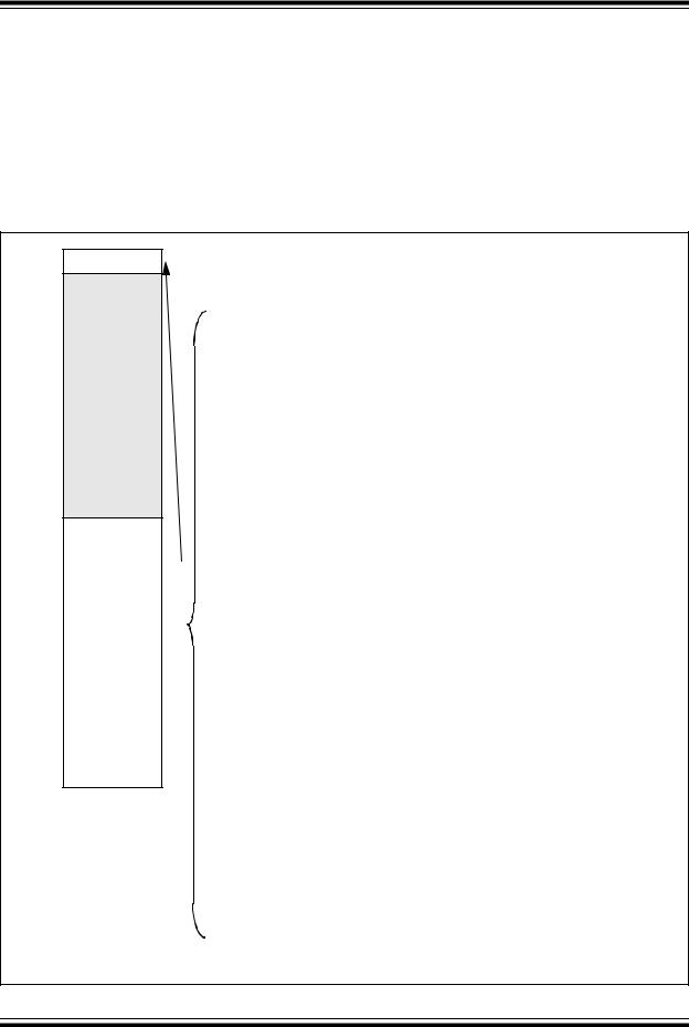
25.5Program Verification and Code Protection
The user program memory is divided into four blocks for PIC18F6527/8527 devices, five blocks for PIC18F6622/8622 devices, six blocks for PIC18F6627/ 8627 devices and eight blocks for PIC18F6722/8722 devices. One of these is a Boot Block of 2, 4 or 8 Kbytes. The remainder of the memory is divided into blocks on binary boundaries.
Each of the blocks has three code protection bits associated with them. They are:
•Code-Protect bit (CPn)
•Write-Protect bit (WRTn)
•External Block Table Read bit (EBTRn)
Figure 25-5 shows the program memory organization for 48, 64, 96 and 128-Kbyte devices and the specific code protection bit associated with each block. The actual locations of the bits are summarized in Table 25-3.
FIGURE 25-5: CODE-PROTECTED PROGRAM MEMORY FOR THE PIC18F8722 FAMILY
000000h
Code Memory
01FFFFh
Unimplemented
Read as ‘0’
200000h
Configuration
and ID
Space
3FFFFFh
|
MEMORY SIZE/DEVICE |
|
|
|
128 Kbytes |
96 Kbytes |
64 Kbytes |
48 Kbytes |
Address |
(PIC18FX722) |
(PIC18FX627) |
(PIC18FX622) |
(PIC18FX527) |
Range |
Boot Block |
Boot Block |
Boot Block |
Boot Block |
|
|
|
|
Block 0 |
Block 0 |
Block 0 |
Block 0 |
|
|
|
|
Block 1 |
Block 1 |
Block 1 |
Block 1 |
|
|
|
|
Block 2 |
Block 2 |
Block 2 |
Block 2 |
|
|
|
|
Block 3 |
Block 3 |
Block 3 |
|
|
|
|
|
Block 4 |
Block 4 |
|
|
|
|
|
Unimplemented |
Block 5 |
Block 5 |
|
|
|
Read ‘0’s |
||
|
|
|
|
|
|
Unimplemented |
|
|
|
Read ‘0’s |
|
Block 6 |
|
|
|
|
|
|
|
|
Unimplemented |
|
|
|
Read ‘0’s |
|
|
Block 7 |
|
|
|
|
|
|
|
|
|
|
|
000000h
0007FFh* or 000FFFh* or 001FFFh*
000800h* or
001000h* or
002000h*
003FFFh
004000h
007FFFh
008000h
00BFFFh
00C000h
00FFFFh
010000h
013FFFh
014000h
017FFFh
018000h
01BFFFh
01C000h
01FFFFh
Note: Sizes of memory areas are not to scale.
*Boot Block size is determined by the BBSIZ<1:0> bits in CONFIG4L.
2004 Microchip Technology Inc.
Preliminary
DS39646B-page 317