

- •LM3S6965 Microcontroller
- •Table of Contents
- •List of Figures
- •List of Tables
- •List of Registers
- •Revision History
- •About This Document
- •Audience
- •About This Manual
- •Related Documents
- •Documentation Conventions
- •1. Architectural Overview
- •1.1. Product Features
- •1.2. Target Applications
- •1.4. Functional Overview
- •1.4.1.1. Processor Core
- •1.4.1.2. System Timer (SysTick)
- •1.4.1.3. Nested Vectored Interrupt Controller (NVIC)
- •1.4.2. Motor Control Peripherals
- •1.4.3. Analog Peripherals
- •1.4.3.2. Analog Comparators
- •1.4.4. Serial Communications Peripherals
- •1.4.4.1. UART
- •1.4.4.4. Ethernet Controller
- •1.4.5. System Peripherals
- •1.4.5.1. Programmable GPIOs
- •1.4.5.2. Four Programmable Timers
- •1.4.5.3. Watchdog Timer
- •1.4.6. Memory Peripherals
- •1.4.6.1. SRAM
- •1.4.6.2. Flash
- •1.4.7. Additional Features
- •1.4.7.1. Memory Map
- •1.4.7.2. JTAG TAP Controller
- •1.4.7.3. System Control and Clocks
- •1.4.7.4. Hibernation Module
- •1.4.8. Hardware Details
- •2.1. Block Diagram
- •2.2. Functional Description
- •2.2.1. Serial Wire and JTAG Debug
- •2.2.2. Embedded Trace Macrocell (ETM)
- •2.2.3. Trace Port Interface Unit (TPIU)
- •2.2.4. ROM Table
- •2.2.5. Memory Protection Unit (MPU)
- •2.2.6. Nested Vectored Interrupt Controller (NVIC)
- •2.2.6.1. Interrupts
- •2.2.6.2. System Timer (SysTick)
- •Functional Description
- •SysTick Control and Status Register
- •SysTick Reload Value Register
- •SysTick Current Value Register
- •SysTick Calibration Value Register
- •3. Memory Map
- •4. Interrupts
- •5. JTAG Interface
- •5.1. Block Diagram
- •5.2. Functional Description
- •5.2.1. JTAG Interface Pins
- •5.2.1.1. Test Reset Input (TRST)
- •5.2.1.2. Test Clock Input (TCK)
- •5.2.1.3. Test Mode Select (TMS)
- •5.2.1.4. Test Data Input (TDI)
- •5.2.1.5. Test Data Output (TDO)
- •5.2.2. JTAG TAP Controller
- •5.2.3. Shift Registers
- •5.2.4. Operational Considerations
- •5.2.4.1. GPIO Functionality
- •Recovering a "Locked" Device
- •5.2.4.2. ARM Serial Wire Debug (SWD)
- •JTAG-to-SWD Switching
- •SWD-to-JTAG Switching
- •5.3. Initialization and Configuration
- •5.4. Register Descriptions
- •5.4.1. Instruction Register (IR)
- •5.4.1.1. EXTEST Instruction
- •5.4.1.2. INTEST Instruction
- •5.4.1.3. SAMPLE/PRELOAD Instruction
- •5.4.1.4. ABORT Instruction
- •5.4.1.5. DPACC Instruction
- •5.4.1.6. APACC Instruction
- •5.4.1.7. IDCODE Instruction
- •5.4.1.8. BYPASS Instruction
- •5.4.2. Data Registers
- •5.4.2.1. IDCODE Data Register
- •5.4.2.2. BYPASS Data Register
- •5.4.2.3. Boundary Scan Data Register
- •5.4.2.4. APACC Data Register
- •5.4.2.5. DPACC Data Register
- •5.4.2.6. ABORT Data Register
- •6. System Control
- •6.1. Functional Description
- •6.1.1. Device Identification
- •6.1.2. Reset Control
- •6.1.2.2. Reset Sources
- •6.1.2.3. RST Pin Assertion
- •6.1.2.6. Software Reset
- •6.1.2.7. Watchdog Timer Reset
- •6.1.3. Power Control
- •6.1.4. Clock Control
- •6.1.4.1. Fundamental Clock Sources
- •6.1.4.2. Crystal Configuration for the Main Oscillator (MOSC)
- •6.1.4.3. Main PLL Frequency Configuration
- •6.1.4.4. PLL Modes
- •6.1.4.5. PLL Operation
- •6.1.5. System Control
- •6.2. Initialization and Configuration
- •6.3. Register Map
- •6.4. Register Descriptions
- •Register 1: Device Identification 0 (DID0), offset 0x000
- •Register 2: Brown-Out Reset Control (PBORCTL), offset 0x030
- •Register 3: LDO Power Control (LDOPCTL), offset 0x034
- •Register 4: Raw Interrupt Status (RIS), offset 0x050
- •Register 5: Interrupt Mask Control (IMC), offset 0x054
- •Register 6: Masked Interrupt Status and Clear (MISC), offset 0x058
- •Register 7: Reset Cause (RESC), offset 0x05C
- •Register 8: Run-Mode Clock Configuration (RCC), offset 0x060
- •Register 9: XTAL to PLL Translation (PLLCFG), offset 0x064
- •Register 10: Run-Mode Clock Configuration 2 (RCC2), offset 0x070
- •Register 11: Deep Sleep Clock Configuration (DSLPCLKCFG), offset 0x144
- •Register 12: Device Identification 1 (DID1), offset 0x004
- •Register 13: Device Capabilities 0 (DC0), offset 0x008
- •Register 14: Device Capabilities 1 (DC1), offset 0x010
- •Register 15: Device Capabilities 2 (DC2), offset 0x014
- •Register 16: Device Capabilities 3 (DC3), offset 0x018
- •Register 17: Device Capabilities 4 (DC4), offset 0x01C
- •Register 18: Run Mode Clock Gating Control Register 0 (RCGC0), offset 0x100
- •Register 19: Sleep Mode Clock Gating Control Register 0 (SCGC0), offset 0x110
- •Register 20: Deep Sleep Mode Clock Gating Control Register 0 (DCGC0), offset 0x120
- •Register 21: Run Mode Clock Gating Control Register 1 (RCGC1), offset 0x104
- •Register 22: Sleep Mode Clock Gating Control Register 1 (SCGC1), offset 0x114
- •Register 23: Deep Sleep Mode Clock Gating Control Register 1 (DCGC1), offset 0x124
- •Register 24: Run Mode Clock Gating Control Register 2 (RCGC2), offset 0x108
- •Register 25: Sleep Mode Clock Gating Control Register 2 (SCGC2), offset 0x118
- •Register 26: Deep Sleep Mode Clock Gating Control Register 2 (DCGC2), offset 0x128
- •Register 27: Software Reset Control 0 (SRCR0), offset 0x040
- •Register 28: Software Reset Control 1 (SRCR1), offset 0x044
- •Register 29: Software Reset Control 2 (SRCR2), offset 0x048
- •7. Hibernation Module
- •7.1. Block Diagram
- •7.2. Functional Description
- •7.2.1. Register Access Timing
- •7.2.2. Clock Source
- •7.2.3. Battery Management
- •7.2.6. Power Control
- •7.2.7. Initiating Hibernate
- •7.2.8. Interrupts and Status
- •7.3. Initialization and Configuration
- •7.3.1. Initialization
- •7.3.2. RTC Match Functionality (No Hibernation)
- •7.4. Register Map
- •7.5. Register Descriptions
- •Register 1: Hibernation RTC Counter (HIBRTCC), offset 0x000
- •Register 2: Hibernation RTC Match 0 (HIBRTCM0), offset 0x004
- •Register 3: Hibernation RTC Match 1 (HIBRTCM1), offset 0x008
- •Register 4: Hibernation RTC Load (HIBRTCLD), offset 0x00C
- •Register 5: Hibernation Control (HIBCTL), offset 0x010
- •Register 6: Hibernation Interrupt Mask (HIBIM), offset 0x014
- •Register 7: Hibernation Raw Interrupt Status (HIBRIS), offset 0x018
- •Register 8: Hibernation Masked Interrupt Status (HIBMIS), offset 0x01C
- •Register 9: Hibernation Interrupt Clear (HIBIC), offset 0x020
- •Register 10: Hibernation RTC Trim (HIBRTCT), offset 0x024
- •8. Internal Memory
- •8.1. Block Diagram
- •8.2. Functional Description
- •8.2.1. SRAM Memory
- •8.2.2. Flash Memory
- •8.2.2.1. Flash Memory Timing
- •8.2.2.2. Flash Memory Protection
- •8.3. Flash Memory Initialization and Configuration
- •8.3.1. Flash Programming
- •8.3.1.3. To perform a mass erase of the flash
- •8.3.2. Nonvolatile Register Programming
- •8.4. Register Map
- •8.5. Flash Register Descriptions (Flash Control Offset)
- •Register 1: Flash Memory Address (FMA), offset 0x000
- •Register 2: Flash Memory Data (FMD), offset 0x004
- •Register 3: Flash Memory Control (FMC), offset 0x008
- •Register 4: Flash Controller Raw Interrupt Status (FCRIS), offset 0x00C
- •Register 5: Flash Controller Interrupt Mask (FCIM), offset 0x010
- •Register 6: Flash Controller Masked Interrupt Status and Clear (FCMISC), offset 0x014
- •8.6. Flash Register Descriptions (System Control Offset)
- •Register 7: USec Reload (USECRL), offset 0x140
- •Register 8: Flash Memory Protection Read Enable 0 (FMPRE0), offset 0x130 and 0x200
- •Register 9: Flash Memory Protection Program Enable 0 (FMPPE0), offset 0x134 and 0x400
- •Register 10: User Debug (USER_DBG), offset 0x1D0
- •Register 11: User Register 0 (USER_REG0), offset 0x1E0
- •Register 12: User Register 1 (USER_REG1), offset 0x1E4
- •Register 13: Flash Memory Protection Read Enable 1 (FMPRE1), offset 0x204
- •Register 14: Flash Memory Protection Read Enable 2 (FMPRE2), offset 0x208
- •Register 15: Flash Memory Protection Read Enable 3 (FMPRE3), offset 0x20C
- •Register 16: Flash Memory Protection Program Enable 1 (FMPPE1), offset 0x404
- •Register 17: Flash Memory Protection Program Enable 2 (FMPPE2), offset 0x408
- •Register 18: Flash Memory Protection Program Enable 3 (FMPPE3), offset 0x40C
- •9. General-Purpose Input/Outputs (GPIOs)
- •9.1. Functional Description
- •9.1.1. Data Control
- •9.1.1.1. Data Direction Operation
- •9.1.1.2. Data Register Operation
- •9.1.2. Interrupt Control
- •9.1.3. Mode Control
- •9.1.4. Commit Control
- •9.1.5. Pad Control
- •9.1.6. Identification
- •9.2. Initialization and Configuration
- •9.3. Register Map
- •9.4. Register Descriptions
- •Register 1: GPIO Data (GPIODATA), offset 0x000
- •Register 2: GPIO Direction (GPIODIR), offset 0x400
- •Register 3: GPIO Interrupt Sense (GPIOIS), offset 0x404
- •Register 4: GPIO Interrupt Both Edges (GPIOIBE), offset 0x408
- •Register 5: GPIO Interrupt Event (GPIOIEV), offset 0x40C
- •Register 6: GPIO Interrupt Mask (GPIOIM), offset 0x410
- •Register 7: GPIO Raw Interrupt Status (GPIORIS), offset 0x414
- •Register 8: GPIO Masked Interrupt Status (GPIOMIS), offset 0x418
- •Register 9: GPIO Interrupt Clear (GPIOICR), offset 0x41C
- •Register 10: GPIO Alternate Function Select (GPIOAFSEL), offset 0x420
- •Register 11: GPIO 2-mA Drive Select (GPIODR2R), offset 0x500
- •Register 12: GPIO 4-mA Drive Select (GPIODR4R), offset 0x504
- •Register 13: GPIO 8-mA Drive Select (GPIODR8R), offset 0x508
- •Register 14: GPIO Open Drain Select (GPIOODR), offset 0x50C
- •Register 15: GPIO Pull-Up Select (GPIOPUR), offset 0x510
- •Register 16: GPIO Pull-Down Select (GPIOPDR), offset 0x514
- •Register 17: GPIO Slew Rate Control Select (GPIOSLR), offset 0x518
- •Register 18: GPIO Digital Enable (GPIODEN), offset 0x51C
- •Register 19: GPIO Lock (GPIOLOCK), offset 0x520
- •Register 20: GPIO Commit (GPIOCR), offset 0x524
- •Register 21: GPIO Peripheral Identification 4 (GPIOPeriphID4), offset 0xFD0
- •Register 22: GPIO Peripheral Identification 5 (GPIOPeriphID5), offset 0xFD4
- •Register 23: GPIO Peripheral Identification 6 (GPIOPeriphID6), offset 0xFD8
- •Register 24: GPIO Peripheral Identification 7 (GPIOPeriphID7), offset 0xFDC
- •Register 25: GPIO Peripheral Identification 0 (GPIOPeriphID0), offset 0xFE0
- •Register 26: GPIO Peripheral Identification 1 (GPIOPeriphID1), offset 0xFE4
- •Register 27: GPIO Peripheral Identification 2 (GPIOPeriphID2), offset 0xFE8
- •Register 28: GPIO Peripheral Identification 3 (GPIOPeriphID3), offset 0xFEC
- •Register 29: GPIO PrimeCell Identification 0 (GPIOPCellID0), offset 0xFF0
- •Register 30: GPIO PrimeCell Identification 1 (GPIOPCellID1), offset 0xFF4
- •Register 31: GPIO PrimeCell Identification 2 (GPIOPCellID2), offset 0xFF8
- •Register 32: GPIO PrimeCell Identification 3 (GPIOPCellID3), offset 0xFFC
- •10. General-Purpose Timers
- •10.1. Block Diagram
- •10.2. Functional Description
- •10.2.1. GPTM Reset Conditions
- •10.2.2.1. 32-Bit One-Shot/Periodic Timer Mode
- •10.2.2.2. 32-Bit Real-Time Clock Timer Mode
- •10.2.3.1. 16-Bit One-Shot/Periodic Timer Mode
- •10.2.3.3. 16-Bit Input Edge Time Mode
- •10.2.3.4. 16-Bit PWM Mode
- •10.3. Initialization and Configuration
- •10.4. Register Map
- •10.5. Register Descriptions
- •Register 1: GPTM Configuration (GPTMCFG), offset 0x000
- •Register 2: GPTM TimerA Mode (GPTMTAMR), offset 0x004
- •Register 3: GPTM TimerB Mode (GPTMTBMR), offset 0x008
- •Register 4: GPTM Control (GPTMCTL), offset 0x00C
- •Register 5: GPTM Interrupt Mask (GPTMIMR), offset 0x018
- •Register 6: GPTM Raw Interrupt Status (GPTMRIS), offset 0x01C
- •Register 7: GPTM Masked Interrupt Status (GPTMMIS), offset 0x020
- •Register 8: GPTM Interrupt Clear (GPTMICR), offset 0x024
- •Register 9: GPTM TimerA Interval Load (GPTMTAILR), offset 0x028
- •Register 10: GPTM TimerB Interval Load (GPTMTBILR), offset 0x02C
- •Register 11: GPTM TimerA Match (GPTMTAMATCHR), offset 0x030
- •Register 12: GPTM TimerB Match (GPTMTBMATCHR), offset 0x034
- •Register 13: GPTM TimerA Prescale (GPTMTAPR), offset 0x038
- •Register 14: GPTM TimerB Prescale (GPTMTBPR), offset 0x03C
- •Register 15: GPTM TimerA Prescale Match (GPTMTAPMR), offset 0x040
- •Register 16: GPTM TimerB Prescale Match (GPTMTBPMR), offset 0x044
- •Register 17: GPTM TimerA (GPTMTAR), offset 0x048
- •Register 18: GPTM TimerB (GPTMTBR), offset 0x04C
- •11. Watchdog Timer
- •11.1. Block Diagram
- •11.2. Functional Description
- •11.3. Initialization and Configuration
- •11.4. Register Map
- •11.5. Register Descriptions
- •Register 1: Watchdog Load (WDTLOAD), offset 0x000
- •Register 2: Watchdog Value (WDTVALUE), offset 0x004
- •Register 3: Watchdog Control (WDTCTL), offset 0x008
- •Register 4: Watchdog Interrupt Clear (WDTICR), offset 0x00C
- •Register 5: Watchdog Raw Interrupt Status (WDTRIS), offset 0x010
- •Register 6: Watchdog Masked Interrupt Status (WDTMIS), offset 0x014
- •Register 7: Watchdog Test (WDTTEST), offset 0x418
- •Register 8: Watchdog Lock (WDTLOCK), offset 0xC00
- •Register 10: Watchdog Peripheral Identification 5 (WDTPeriphID5), offset 0xFD4
- •Register 11: Watchdog Peripheral Identification 6 (WDTPeriphID6), offset 0xFD8
- •Register 12: Watchdog Peripheral Identification 7 (WDTPeriphID7), offset 0xFDC
- •Register 13: Watchdog Peripheral Identification 0 (WDTPeriphID0), offset 0xFE0
- •Register 14: Watchdog Peripheral Identification 1 (WDTPeriphID1), offset 0xFE4
- •Register 15: Watchdog Peripheral Identification 2 (WDTPeriphID2), offset 0xFE8
- •Register 16: Watchdog Peripheral Identification 3 (WDTPeriphID3), offset 0xFEC
- •Register 17: Watchdog PrimeCell Identification 0 (WDTPCellID0), offset 0xFF0
- •Register 18: Watchdog PrimeCell Identification 1 (WDTPCellID1), offset 0xFF4
- •Register 19: Watchdog PrimeCell Identification 2 (WDTPCellID2), offset 0xFF8
- •12. Analog-to-Digital Converter (ADC)
- •12.1. Block Diagram
- •12.2. Functional Description
- •12.2.1. Sample Sequencers
- •12.2.2. Module Control
- •12.2.2.1. Interrupts
- •12.2.2.2. Prioritization
- •12.2.2.3. Sampling Events
- •12.2.3. Hardware Sample Averaging Circuit
- •12.2.5. Differential Sampling
- •12.2.6. Test Modes
- •12.2.7. Internal Temperature Sensor
- •12.3. Initialization and Configuration
- •12.3.1. Module Initialization
- •12.3.2. Sample Sequencer Configuration
- •12.4. Register Map
- •12.5. Register Descriptions
- •Register 1: ADC Active Sample Sequencer (ADCACTSS), offset 0x000
- •Register 2: ADC Raw Interrupt Status (ADCRIS), offset 0x004
- •Register 3: ADC Interrupt Mask (ADCIM), offset 0x008
- •Register 4: ADC Interrupt Status and Clear (ADCISC), offset 0x00C
- •Register 5: ADC Overflow Status (ADCOSTAT), offset 0x010
- •Register 6: ADC Event Multiplexer Select (ADCEMUX), offset 0x014
- •Register 7: ADC Underflow Status (ADCUSTAT), offset 0x018
- •Register 8: ADC Sample Sequencer Priority (ADCSSPRI), offset 0x020
- •Register 9: ADC Processor Sample Sequence Initiate (ADCPSSI), offset 0x028
- •Register 10: ADC Sample Averaging Control (ADCSAC), offset 0x030
- •Register 12: ADC Sample Sequence Control 0 (ADCSSCTL0), offset 0x044
- •Register 16: ADC Sample Sequence Result FIFO 3 (ADCSSFIFO3), offset 0x0A8
- •Register 17: ADC Sample Sequence FIFO 0 Status (ADCSSFSTAT0), offset 0x04C
- •Register 18: ADC Sample Sequence FIFO 1 Status (ADCSSFSTAT1), offset 0x06C
- •Register 19: ADC Sample Sequence FIFO 2 Status (ADCSSFSTAT2), offset 0x08C
- •Register 20: ADC Sample Sequence FIFO 3 Status (ADCSSFSTAT3), offset 0x0AC
- •Register 21: ADC Sample Sequence Input Multiplexer Select 1 (ADCSSMUX1), offset 0x060
- •Register 22: ADC Sample Sequence Input Multiplexer Select 2 (ADCSSMUX2), offset 0x080
- •Register 23: ADC Sample Sequence Control 1 (ADCSSCTL1), offset 0x064
- •Register 24: ADC Sample Sequence Control 2 (ADCSSCTL2), offset 0x084
- •Register 25: ADC Sample Sequence Input Multiplexer Select 3 (ADCSSMUX3), offset 0x0A0
- •Register 26: ADC Sample Sequence Control 3 (ADCSSCTL3), offset 0x0A4
- •Register 27: ADC Test Mode Loopback (ADCTMLB), offset 0x100
- •13. Universal Asynchronous Receivers/Transmitters (UARTs)
- •13.1. Block Diagram
- •13.2. Functional Description
- •13.2.1. Transmit/Receive Logic
- •13.2.3. Data Transmission
- •13.2.4. Serial IR (SIR)
- •13.2.5. FIFO Operation
- •13.2.6. Interrupts
- •13.2.7. Loopback Operation
- •13.2.8. IrDA SIR block
- •13.3. Initialization and Configuration
- •13.4. Register Map
- •13.5. Register Descriptions
- •Register 1: UART Data (UARTDR), offset 0x000
- •Register 3: UART Flag (UARTFR), offset 0x018
- •Register 4: UART IrDA Low-Power Register (UARTILPR), offset 0x020
- •Register 5: UART Integer Baud-Rate Divisor (UARTIBRD), offset 0x024
- •Register 6: UART Fractional Baud-Rate Divisor (UARTFBRD), offset 0x028
- •Register 7: UART Line Control (UARTLCRH), offset 0x02C
- •Register 8: UART Control (UARTCTL), offset 0x030
- •Register 9: UART Interrupt FIFO Level Select (UARTIFLS), offset 0x034
- •Register 10: UART Interrupt Mask (UARTIM), offset 0x038
- •Register 11: UART Raw Interrupt Status (UARTRIS), offset 0x03C
- •Register 12: UART Masked Interrupt Status (UARTMIS), offset 0x040
- •Register 13: UART Interrupt Clear (UARTICR), offset 0x044
- •Register 14: UART Peripheral Identification 4 (UARTPeriphID4), offset 0xFD0
- •Register 15: UART Peripheral Identification 5 (UARTPeriphID5), offset 0xFD4
- •Register 16: UART Peripheral Identification 6 (UARTPeriphID6), offset 0xFD8
- •Register 17: UART Peripheral Identification 7 (UARTPeriphID7), offset 0xFDC
- •Register 18: UART Peripheral Identification 0 (UARTPeriphID0), offset 0xFE0
- •Register 19: UART Peripheral Identification 1 (UARTPeriphID1), offset 0xFE4
- •Register 20: UART Peripheral Identification 2 (UARTPeriphID2), offset 0xFE8
- •Register 21: UART Peripheral Identification 3 (UARTPeriphID3), offset 0xFEC
- •Register 22: UART PrimeCell Identification 0 (UARTPCellID0), offset 0xFF0
- •Register 23: UART PrimeCell Identification 1 (UARTPCellID1), offset 0xFF4
- •Register 24: UART PrimeCell Identification 2 (UARTPCellID2), offset 0xFF8
- •Register 25: UART PrimeCell Identification 3 (UARTPCellID3), offset 0xFFC
- •14. Synchronous Serial Interface (SSI)
- •14.1. Block Diagram
- •14.2. Functional Description
- •14.2.1. Bit Rate Generation
- •14.2.2. FIFO Operation
- •14.2.2.1. Transmit FIFO
- •14.2.2.2. Receive FIFO
- •14.2.3. Interrupts
- •14.2.4. Frame Formats
- •14.2.4.1. Texas Instruments Synchronous Serial Frame Format
- •14.2.4.2. Freescale SPI Frame Format
- •SPO Clock Polarity Bit
- •SPH Phase Control Bit
- •14.2.4.3. Freescale SPI Frame Format with SPO=0 and SPH=0
- •14.2.4.4. Freescale SPI Frame Format with SPO=0 and SPH=1
- •14.2.4.5. Freescale SPI Frame Format with SPO=1 and SPH=0
- •14.2.4.6. Freescale SPI Frame Format with SPO=1 and SPH=1
- •14.2.4.7. MICROWIRE Frame Format
- •14.3. Initialization and Configuration
- •14.4. Register Map
- •14.5. Register Descriptions
- •Register 1: SSI Control 0 (SSICR0), offset 0x000
- •Register 2: SSI Control 1 (SSICR1), offset 0x004
- •Register 3: SSI Data (SSIDR), offset 0x008
- •Register 4: SSI Status (SSISR), offset 0x00C
- •Register 5: SSI Clock Prescale (SSICPSR), offset 0x010
- •Register 6: SSI Interrupt Mask (SSIIM), offset 0x014
- •Register 7: SSI Raw Interrupt Status (SSIRIS), offset 0x018
- •Register 8: SSI Masked Interrupt Status (SSIMIS), offset 0x01C
- •Register 9: SSI Interrupt Clear (SSIICR), offset 0x020
- •Register 10: SSI Peripheral Identification 4 (SSIPeriphID4), offset 0xFD0
- •Register 11: SSI Peripheral Identification 5 (SSIPeriphID5), offset 0xFD4
- •Register 12: SSI Peripheral Identification 6 (SSIPeriphID6), offset 0xFD8
- •Register 13: SSI Peripheral Identification 7 (SSIPeriphID7), offset 0xFDC
- •Register 14: SSI Peripheral Identification 0 (SSIPeriphID0), offset 0xFE0
- •Register 15: SSI Peripheral Identification 1 (SSIPeriphID1), offset 0xFE4
- •Register 16: SSI Peripheral Identification 2 (SSIPeriphID2), offset 0xFE8
- •Register 17: SSI Peripheral Identification 3 (SSIPeriphID3), offset 0xFEC
- •Register 18: SSI PrimeCell Identification 0 (SSIPCellID0), offset 0xFF0
- •Register 19: SSI PrimeCell Identification 1 (SSIPCellID1), offset 0xFF4
- •Register 20: SSI PrimeCell Identification 2 (SSIPCellID2), offset 0xFF8
- •Register 21: SSI PrimeCell Identification 3 (SSIPCellID3), offset 0xFFC
- •15. Inter-Integrated Circuit (I2C) Interface
- •15.1. Block Diagram
- •15.2. Functional Description
- •15.2.1.1. START and STOP Conditions
- •15.2.1.2. Data Format with 7-Bit Address
- •15.2.1.3. Data Validity
- •15.2.1.4. Acknowledge
- •15.2.1.5. Arbitration
- •15.2.2. Available Speed Modes
- •15.2.3. Interrupts
- •15.2.3.1. I2C Master Interrupts
- •15.2.3.2. I2C Slave Interrupts
- •15.2.4. Loopback Operation
- •15.2.5. Command Sequence Flow Charts
- •15.2.5.1. I2C Master Command Sequences
- •15.2.5.2. I2C Slave Command Sequences
- •15.3. Initialization and Configuration
- •15.4. Register Map
- •Register 1: I2C Master Slave Address (I2CMSA), offset 0x000
- •Register 2: I2C Master Control/Status (I2CMCS), offset 0x004
- •Register 3: I2C Master Data (I2CMDR), offset 0x008
- •Register 4: I2C Master Timer Period (I2CMTPR), offset 0x00C
- •Register 5: I2C Master Interrupt Mask (I2CMIMR), offset 0x010
- •Register 6: I2C Master Raw Interrupt Status (I2CMRIS), offset 0x014
- •Register 7: I2C Master Masked Interrupt Status (I2CMMIS), offset 0x018
- •Register 8: I2C Master Interrupt Clear (I2CMICR), offset 0x01C
- •Register 9: I2C Master Configuration (I2CMCR), offset 0x020
- •Register 10: I2C Slave Own Address (I2CSOAR), offset 0x000
- •Register 11: I2C Slave Control/Status (I2CSCSR), offset 0x004
- •Register 12: I2C Slave Data (I2CSDR), offset 0x008
- •Register 13: I2C Slave Interrupt Mask (I2CSIMR), offset 0x00C
- •Register 14: I2C Slave Raw Interrupt Status (I2CSRIS), offset 0x010
- •Register 15: I2C Slave Masked Interrupt Status (I2CSMIS), offset 0x014
- •Register 16: I2C Slave Interrupt Clear (I2CSICR), offset 0x018
- •16. Ethernet Controller
- •16.1. Block Diagram
- •16.2. Functional Description
- •16.2.1. MAC Operation
- •16.2.1.1. Ethernet Frame Format
- •16.2.1.2. MAC Layer FIFOs
- •16.2.1.3. Ethernet Transmission Options
- •16.2.1.4. Ethernet Reception Options
- •16.2.2. Internal MII Operation
- •16.2.3. PHY Operation
- •16.2.3.1. Clock Selection
- •16.2.3.2. Auto-Negotiation
- •16.2.3.3. Polarity Correction
- •16.2.3.4. MDI/MDI-X Configuration
- •16.2.3.5. LED Indicators
- •16.2.4. Interrupts
- •16.3. Initialization and Configuration
- •16.4. Ethernet Register Map
- •16.5. Ethernet MAC Register Descriptions
- •Register 1: Ethernet MAC Raw Interrupt Status/Acknowledge (MACRIS/MACIACK), offset 0x000
- •Register 2: Ethernet MAC Interrupt Mask (MACIM), offset 0x004
- •Register 3: Ethernet MAC Receive Control (MACRCTL), offset 0x008
- •Register 4: Ethernet MAC Transmit Control (MACTCTL), offset 0x00C
- •Register 5: Ethernet MAC Data (MACDATA), offset 0x010
- •Register 6: Ethernet MAC Individual Address 0 (MACIA0), offset 0x014
- •Register 7: Ethernet MAC Individual Address 1 (MACIA1), offset 0x018
- •Register 8: Ethernet MAC Threshold (MACTHR), offset 0x01C
- •Register 9: Ethernet MAC Management Control (MACMCTL), offset 0x020
- •Register 10: Ethernet MAC Management Divider (MACMDV), offset 0x024
- •Register 11: Ethernet MAC Management Transmit Data (MACMTXD), offset 0x02C
- •Register 12: Ethernet MAC Management Receive Data (MACMRXD), offset 0x030
- •Register 13: Ethernet MAC Number of Packets (MACNP), offset 0x034
- •Register 14: Ethernet MAC Transmission Request (MACTR), offset 0x038
- •16.6. MII Management Register Descriptions
- •Register 15: Ethernet PHY Management Register 0 – Control (MR0), address 0x00
- •Register 16: Ethernet PHY Management Register 1 – Status (MR1), address 0x01
- •Register 17: Ethernet PHY Management Register 2 – PHY Identifier 1 (MR2), address 0x02
- •Register 18: Ethernet PHY Management Register 3 – PHY Identifier 2 (MR3), address 0x03
- •Register 19: Ethernet PHY Management Register 4 – Auto-Negotiation Advertisement (MR4), address 0x04
- •Register 20: Ethernet PHY Management Register 5 – Auto-Negotiation Link Partner Base Page Ability (MR5), address 0x05
- •Register 21: Ethernet PHY Management Register 6 – Auto-Negotiation Expansion (MR6), address 0x06
- •Register 23: Ethernet PHY Management Register 17 – Interrupt Control/Status (MR17), address 0x11
- •Register 24: Ethernet PHY Management Register 18 – Diagnostic (MR18), address 0x12
- •Register 25: Ethernet PHY Management Register 19 – Transceiver Control (MR19), address 0x13
- •Register 26: Ethernet PHY Management Register 23 – LED Configuration (MR23), address 0x17
- •17. Analog Comparators
- •17.1. Block Diagram
- •17.2. Functional Description
- •17.2.1. Internal Reference Programming
- •17.3. Initialization and Configuration
- •17.4. Register Map
- •17.5. Register Descriptions
- •Register 1: Analog Comparator Masked Interrupt Status (ACMIS), offset 0x000
- •Register 2: Analog Comparator Raw Interrupt Status (ACRIS), offset 0x004
- •Register 3: Analog Comparator Interrupt Enable (ACINTEN), offset 0x008
- •Register 5: Analog Comparator Status 0 (ACSTAT0), offset 0x020
- •Register 6: Analog Comparator Status 1 (ACSTAT1), offset 0x040
- •Register 7: Analog Comparator Control 0 (ACCTL0), offset 0x024
- •Register 8: Analog Comparator Control 1 (ACCTL1), offset 0x044
- •18. Pulse Width Modulator (PWM)
- •18.1. Block Diagram
- •18.2. Functional Description
- •18.2.1. PWM Timer
- •18.2.2. PWM Comparators
- •18.2.3. PWM Signal Generator
- •18.2.6. Synchronization Methods
- •18.2.7. Fault Conditions
- •18.2.8. Output Control Block
- •18.3. Initialization and Configuration
- •18.4. Register Map
- •18.5. Register Descriptions
- •Register 1: PWM Master Control (PWMCTL), offset 0x000
- •Register 2: PWM Time Base Sync (PWMSYNC), offset 0x004
- •Register 3: PWM Output Enable (PWMENABLE), offset 0x008
- •Register 4: PWM Output Inversion (PWMINVERT), offset 0x00C
- •Register 5: PWM Output Fault (PWMFAULT), offset 0x010
- •Register 6: PWM Interrupt Enable (PWMINTEN), offset 0x014
- •Register 7: PWM Raw Interrupt Status (PWMRIS), offset 0x018
- •Register 8: PWM Interrupt Status and Clear (PWMISC), offset 0x01C
- •Register 9: PWM Status (PWMSTATUS), offset 0x020
- •Register 10: PWM0 Control (PWM0CTL), offset 0x040
- •Register 11: PWM1 Control (PWM1CTL), offset 0x080
- •Register 12: PWM2 Control (PWM2CTL), offset 0x0C0
- •Register 22: PWM0 Load (PWM0LOAD), offset 0x050
- •Register 23: PWM1 Load (PWM1LOAD), offset 0x090
- •Register 24: PWM2 Load (PWM2LOAD), offset 0x0D0
- •Register 25: PWM0 Counter (PWM0COUNT), offset 0x054
- •Register 26: PWM1 Counter (PWM1COUNT), offset 0x094
- •Register 27: PWM2 Counter (PWM2COUNT), offset 0x0D4
- •Register 28: PWM0 Compare A (PWM0CMPA), offset 0x058
- •Register 29: PWM1 Compare A (PWM1CMPA), offset 0x098
- •Register 30: PWM2 Compare A (PWM2CMPA), offset 0x0D8
- •Register 31: PWM0 Compare B (PWM0CMPB), offset 0x05C
- •Register 32: PWM1 Compare B (PWM1CMPB), offset 0x09C
- •Register 33: PWM2 Compare B (PWM2CMPB), offset 0x0DC
- •Register 40: PWM0 Dead-Band Control (PWM0DBCTL), offset 0x068
- •Register 41: PWM1 Dead-Band Control (PWM1DBCTL), offset 0x0A8
- •Register 42: PWM2 Dead-Band Control (PWM2DBCTL), offset 0x0E8
- •Register 43: PWM0 Dead-Band Rising-Edge Delay (PWM0DBRISE), offset 0x06C
- •Register 44: PWM1 Dead-Band Rising-Edge Delay (PWM1DBRISE), offset 0x0AC
- •Register 45: PWM2 Dead-Band Rising-Edge Delay (PWM2DBRISE), offset 0x0EC
- •Register 46: PWM0 Dead-Band Falling-Edge-Delay (PWM0DBFALL), offset 0x070
- •Register 47: PWM1 Dead-Band Falling-Edge-Delay (PWM1DBFALL), offset 0x0B0
- •Register 48: PWM2 Dead-Band Falling-Edge-Delay (PWM2DBFALL), offset 0x0F0
- •19. Quadrature Encoder Interface (QEI)
- •19.1. Block Diagram
- •19.2. Functional Description
- •19.3. Initialization and Configuration
- •19.4. Register Map
- •19.5. Register Descriptions
- •Register 1: QEI Control (QEICTL), offset 0x000
- •Register 2: QEI Status (QEISTAT), offset 0x004
- •Register 3: QEI Position (QEIPOS), offset 0x008
- •Register 4: QEI Maximum Position (QEIMAXPOS), offset 0x00C
- •Register 5: QEI Timer Load (QEILOAD), offset 0x010
- •Register 6: QEI Timer (QEITIME), offset 0x014
- •Register 7: QEI Velocity Counter (QEICOUNT), offset 0x018
- •Register 8: QEI Velocity (QEISPEED), offset 0x01C
- •Register 9: QEI Interrupt Enable (QEIINTEN), offset 0x020
- •Register 10: QEI Raw Interrupt Status (QEIRIS), offset 0x024
- •Register 11: QEI Interrupt Status and Clear (QEIISC), offset 0x028
- •20. Pin Diagram
- •21. Signal Tables
- •22. Operating Characteristics
- •23. Electrical Characteristics
- •23.1. DC Characteristics
- •23.1.1. Maximum Ratings
- •23.1.2. Recommended DC Operating Conditions
- •23.1.4. Power Specifications
- •23.1.5. Flash Memory Characteristics
- •23.1.6. Hibernation
- •23.2. AC Characteristics
- •23.2.1. Load Conditions
- •23.2.2. Clocks
- •23.2.3. JTAG and Boundary Scan
- •23.2.4. Reset
- •23.2.5. Hibernation Module
- •23.2.8. Synchronous Serial Interface (SSI)
- •23.2.10. Ethernet Controller
- •23.2.11. Analog Comparator
- •24. Package Information
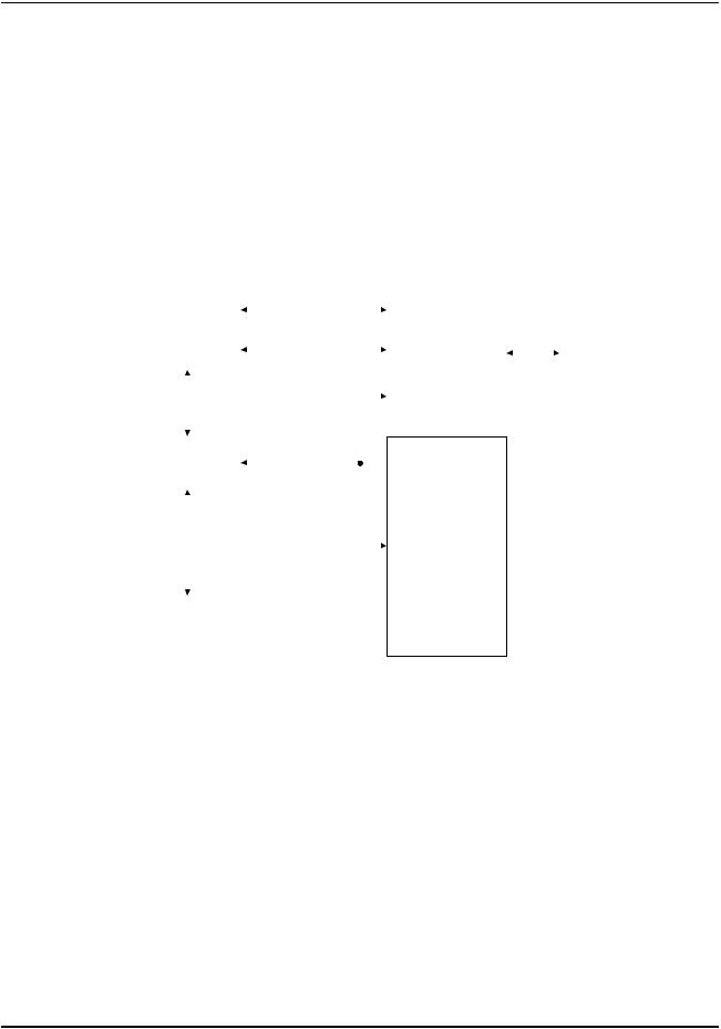
Internal Memory
8Internal Memory
TheLM3S6965microcontrollercomeswith64KBofbit-bandedSRAMand256KBofflashmemory. The flash controller provides a user-friendly interface, making flash programming a simple task. Flash protection can be applied to the flash memory on a 2-KB block basis.
8.1Block Diagram
Figure 8-1 on page 152 illustrates the Flash functions. The dashed boxes in the figure indicate registers residing in the System Control module rather than the Flash Control module.
Figure 8-1. Flash Block Diagram
|
|
Icode |
|
Flash Control |
|
|
||
Cortex-M3 |
Bus |
|
|
|
|
|
||
Dcode |
|
FMA |
|
|
|
|||
|
|
|
FMD |
|
|
Flash Array |
||
|
|
Bus |
|
FMC |
|
|
||
|
|
|
||||||
|
|
|
|
|
FCRIS |
|
|
|
|
|
|
|
|
|
|
|
|
System |
Bus |
|
FCIM |
|
|
|
||
|
|
|
|
|||||
|
FCMISC |
|
|
|
||||
|
|
|
|
|
|
|
|
|
|
|
|
|
|
|
|
|
|
|
|
|
|
|
Flash Protection |
|
|
|
Bridge |
|
|
|
|
|
|||
|
|
|
|
|
|
|
||
|
|
|
|
|
|
|
||
|
|
|
|
|
FMPREn |
|
|
|
|
|
|
|
|
FMPPEn |
|
|
|
|
|
|
|
|
|
|
||
|
|
|
|
|
Flash Timing |
|
|
|
|
|
|
|
|
|
|
|
|
|
|
|
|
|
|
|
|
|
|
|
|
|
|
USECRL |
|
|
|
|
|
|
|
|
User Registers |
|
|
|
|
|
|
|
|
|
|
|
|
SRAM Array |
|
|
|
USER_DBG |
|
|
||
|
|
|
USER_REG0 |
|
|
|
||
|
|
|
|
|
|
|
|
|
|
|
|
|
|
USER_REG1 |
|
|
|
8.2Functional Description
This section describes the functionality of the SRAM and Flash memories.
8.2.1SRAM Memory
TheinternalSRAMoftheStellaris® devicesislocatedataddress0x2000.0000ofthedevicememory map. To reduce the number of time consuming read-modify-write (RMW) operations, ARM has introduced bit-banding technology in the Cortex-M3 processor. With a bit-band-enabled processor, certainregionsinthememorymap(SRAMandperipheralspace)canuseaddressaliasestoaccess individual bits in a single, atomic operation.
The bit-band alias is calculated by using the formula:
bit-band alias = bit-band base + (byte offset * 32) + (bit number * 4)
For example, if bit 3 at address 0x2000.1000 is to be modified, the bit-band alias is calculated as:
0x2200.0000 + (0x1000 * 32) + (3 * 4) = 0x2202.000C
152 |
November 16, 2008 |
Preliminary