

- •LM3S6965 Microcontroller
- •Table of Contents
- •List of Figures
- •List of Tables
- •List of Registers
- •Revision History
- •About This Document
- •Audience
- •About This Manual
- •Related Documents
- •Documentation Conventions
- •1. Architectural Overview
- •1.1. Product Features
- •1.2. Target Applications
- •1.4. Functional Overview
- •1.4.1.1. Processor Core
- •1.4.1.2. System Timer (SysTick)
- •1.4.1.3. Nested Vectored Interrupt Controller (NVIC)
- •1.4.2. Motor Control Peripherals
- •1.4.3. Analog Peripherals
- •1.4.3.2. Analog Comparators
- •1.4.4. Serial Communications Peripherals
- •1.4.4.1. UART
- •1.4.4.4. Ethernet Controller
- •1.4.5. System Peripherals
- •1.4.5.1. Programmable GPIOs
- •1.4.5.2. Four Programmable Timers
- •1.4.5.3. Watchdog Timer
- •1.4.6. Memory Peripherals
- •1.4.6.1. SRAM
- •1.4.6.2. Flash
- •1.4.7. Additional Features
- •1.4.7.1. Memory Map
- •1.4.7.2. JTAG TAP Controller
- •1.4.7.3. System Control and Clocks
- •1.4.7.4. Hibernation Module
- •1.4.8. Hardware Details
- •2.1. Block Diagram
- •2.2. Functional Description
- •2.2.1. Serial Wire and JTAG Debug
- •2.2.2. Embedded Trace Macrocell (ETM)
- •2.2.3. Trace Port Interface Unit (TPIU)
- •2.2.4. ROM Table
- •2.2.5. Memory Protection Unit (MPU)
- •2.2.6. Nested Vectored Interrupt Controller (NVIC)
- •2.2.6.1. Interrupts
- •2.2.6.2. System Timer (SysTick)
- •Functional Description
- •SysTick Control and Status Register
- •SysTick Reload Value Register
- •SysTick Current Value Register
- •SysTick Calibration Value Register
- •3. Memory Map
- •4. Interrupts
- •5. JTAG Interface
- •5.1. Block Diagram
- •5.2. Functional Description
- •5.2.1. JTAG Interface Pins
- •5.2.1.1. Test Reset Input (TRST)
- •5.2.1.2. Test Clock Input (TCK)
- •5.2.1.3. Test Mode Select (TMS)
- •5.2.1.4. Test Data Input (TDI)
- •5.2.1.5. Test Data Output (TDO)
- •5.2.2. JTAG TAP Controller
- •5.2.3. Shift Registers
- •5.2.4. Operational Considerations
- •5.2.4.1. GPIO Functionality
- •Recovering a "Locked" Device
- •5.2.4.2. ARM Serial Wire Debug (SWD)
- •JTAG-to-SWD Switching
- •SWD-to-JTAG Switching
- •5.3. Initialization and Configuration
- •5.4. Register Descriptions
- •5.4.1. Instruction Register (IR)
- •5.4.1.1. EXTEST Instruction
- •5.4.1.2. INTEST Instruction
- •5.4.1.3. SAMPLE/PRELOAD Instruction
- •5.4.1.4. ABORT Instruction
- •5.4.1.5. DPACC Instruction
- •5.4.1.6. APACC Instruction
- •5.4.1.7. IDCODE Instruction
- •5.4.1.8. BYPASS Instruction
- •5.4.2. Data Registers
- •5.4.2.1. IDCODE Data Register
- •5.4.2.2. BYPASS Data Register
- •5.4.2.3. Boundary Scan Data Register
- •5.4.2.4. APACC Data Register
- •5.4.2.5. DPACC Data Register
- •5.4.2.6. ABORT Data Register
- •6. System Control
- •6.1. Functional Description
- •6.1.1. Device Identification
- •6.1.2. Reset Control
- •6.1.2.2. Reset Sources
- •6.1.2.3. RST Pin Assertion
- •6.1.2.6. Software Reset
- •6.1.2.7. Watchdog Timer Reset
- •6.1.3. Power Control
- •6.1.4. Clock Control
- •6.1.4.1. Fundamental Clock Sources
- •6.1.4.2. Crystal Configuration for the Main Oscillator (MOSC)
- •6.1.4.3. Main PLL Frequency Configuration
- •6.1.4.4. PLL Modes
- •6.1.4.5. PLL Operation
- •6.1.5. System Control
- •6.2. Initialization and Configuration
- •6.3. Register Map
- •6.4. Register Descriptions
- •Register 1: Device Identification 0 (DID0), offset 0x000
- •Register 2: Brown-Out Reset Control (PBORCTL), offset 0x030
- •Register 3: LDO Power Control (LDOPCTL), offset 0x034
- •Register 4: Raw Interrupt Status (RIS), offset 0x050
- •Register 5: Interrupt Mask Control (IMC), offset 0x054
- •Register 6: Masked Interrupt Status and Clear (MISC), offset 0x058
- •Register 7: Reset Cause (RESC), offset 0x05C
- •Register 8: Run-Mode Clock Configuration (RCC), offset 0x060
- •Register 9: XTAL to PLL Translation (PLLCFG), offset 0x064
- •Register 10: Run-Mode Clock Configuration 2 (RCC2), offset 0x070
- •Register 11: Deep Sleep Clock Configuration (DSLPCLKCFG), offset 0x144
- •Register 12: Device Identification 1 (DID1), offset 0x004
- •Register 13: Device Capabilities 0 (DC0), offset 0x008
- •Register 14: Device Capabilities 1 (DC1), offset 0x010
- •Register 15: Device Capabilities 2 (DC2), offset 0x014
- •Register 16: Device Capabilities 3 (DC3), offset 0x018
- •Register 17: Device Capabilities 4 (DC4), offset 0x01C
- •Register 18: Run Mode Clock Gating Control Register 0 (RCGC0), offset 0x100
- •Register 19: Sleep Mode Clock Gating Control Register 0 (SCGC0), offset 0x110
- •Register 20: Deep Sleep Mode Clock Gating Control Register 0 (DCGC0), offset 0x120
- •Register 21: Run Mode Clock Gating Control Register 1 (RCGC1), offset 0x104
- •Register 22: Sleep Mode Clock Gating Control Register 1 (SCGC1), offset 0x114
- •Register 23: Deep Sleep Mode Clock Gating Control Register 1 (DCGC1), offset 0x124
- •Register 24: Run Mode Clock Gating Control Register 2 (RCGC2), offset 0x108
- •Register 25: Sleep Mode Clock Gating Control Register 2 (SCGC2), offset 0x118
- •Register 26: Deep Sleep Mode Clock Gating Control Register 2 (DCGC2), offset 0x128
- •Register 27: Software Reset Control 0 (SRCR0), offset 0x040
- •Register 28: Software Reset Control 1 (SRCR1), offset 0x044
- •Register 29: Software Reset Control 2 (SRCR2), offset 0x048
- •7. Hibernation Module
- •7.1. Block Diagram
- •7.2. Functional Description
- •7.2.1. Register Access Timing
- •7.2.2. Clock Source
- •7.2.3. Battery Management
- •7.2.6. Power Control
- •7.2.7. Initiating Hibernate
- •7.2.8. Interrupts and Status
- •7.3. Initialization and Configuration
- •7.3.1. Initialization
- •7.3.2. RTC Match Functionality (No Hibernation)
- •7.4. Register Map
- •7.5. Register Descriptions
- •Register 1: Hibernation RTC Counter (HIBRTCC), offset 0x000
- •Register 2: Hibernation RTC Match 0 (HIBRTCM0), offset 0x004
- •Register 3: Hibernation RTC Match 1 (HIBRTCM1), offset 0x008
- •Register 4: Hibernation RTC Load (HIBRTCLD), offset 0x00C
- •Register 5: Hibernation Control (HIBCTL), offset 0x010
- •Register 6: Hibernation Interrupt Mask (HIBIM), offset 0x014
- •Register 7: Hibernation Raw Interrupt Status (HIBRIS), offset 0x018
- •Register 8: Hibernation Masked Interrupt Status (HIBMIS), offset 0x01C
- •Register 9: Hibernation Interrupt Clear (HIBIC), offset 0x020
- •Register 10: Hibernation RTC Trim (HIBRTCT), offset 0x024
- •8. Internal Memory
- •8.1. Block Diagram
- •8.2. Functional Description
- •8.2.1. SRAM Memory
- •8.2.2. Flash Memory
- •8.2.2.1. Flash Memory Timing
- •8.2.2.2. Flash Memory Protection
- •8.3. Flash Memory Initialization and Configuration
- •8.3.1. Flash Programming
- •8.3.1.3. To perform a mass erase of the flash
- •8.3.2. Nonvolatile Register Programming
- •8.4. Register Map
- •8.5. Flash Register Descriptions (Flash Control Offset)
- •Register 1: Flash Memory Address (FMA), offset 0x000
- •Register 2: Flash Memory Data (FMD), offset 0x004
- •Register 3: Flash Memory Control (FMC), offset 0x008
- •Register 4: Flash Controller Raw Interrupt Status (FCRIS), offset 0x00C
- •Register 5: Flash Controller Interrupt Mask (FCIM), offset 0x010
- •Register 6: Flash Controller Masked Interrupt Status and Clear (FCMISC), offset 0x014
- •8.6. Flash Register Descriptions (System Control Offset)
- •Register 7: USec Reload (USECRL), offset 0x140
- •Register 8: Flash Memory Protection Read Enable 0 (FMPRE0), offset 0x130 and 0x200
- •Register 9: Flash Memory Protection Program Enable 0 (FMPPE0), offset 0x134 and 0x400
- •Register 10: User Debug (USER_DBG), offset 0x1D0
- •Register 11: User Register 0 (USER_REG0), offset 0x1E0
- •Register 12: User Register 1 (USER_REG1), offset 0x1E4
- •Register 13: Flash Memory Protection Read Enable 1 (FMPRE1), offset 0x204
- •Register 14: Flash Memory Protection Read Enable 2 (FMPRE2), offset 0x208
- •Register 15: Flash Memory Protection Read Enable 3 (FMPRE3), offset 0x20C
- •Register 16: Flash Memory Protection Program Enable 1 (FMPPE1), offset 0x404
- •Register 17: Flash Memory Protection Program Enable 2 (FMPPE2), offset 0x408
- •Register 18: Flash Memory Protection Program Enable 3 (FMPPE3), offset 0x40C
- •9. General-Purpose Input/Outputs (GPIOs)
- •9.1. Functional Description
- •9.1.1. Data Control
- •9.1.1.1. Data Direction Operation
- •9.1.1.2. Data Register Operation
- •9.1.2. Interrupt Control
- •9.1.3. Mode Control
- •9.1.4. Commit Control
- •9.1.5. Pad Control
- •9.1.6. Identification
- •9.2. Initialization and Configuration
- •9.3. Register Map
- •9.4. Register Descriptions
- •Register 1: GPIO Data (GPIODATA), offset 0x000
- •Register 2: GPIO Direction (GPIODIR), offset 0x400
- •Register 3: GPIO Interrupt Sense (GPIOIS), offset 0x404
- •Register 4: GPIO Interrupt Both Edges (GPIOIBE), offset 0x408
- •Register 5: GPIO Interrupt Event (GPIOIEV), offset 0x40C
- •Register 6: GPIO Interrupt Mask (GPIOIM), offset 0x410
- •Register 7: GPIO Raw Interrupt Status (GPIORIS), offset 0x414
- •Register 8: GPIO Masked Interrupt Status (GPIOMIS), offset 0x418
- •Register 9: GPIO Interrupt Clear (GPIOICR), offset 0x41C
- •Register 10: GPIO Alternate Function Select (GPIOAFSEL), offset 0x420
- •Register 11: GPIO 2-mA Drive Select (GPIODR2R), offset 0x500
- •Register 12: GPIO 4-mA Drive Select (GPIODR4R), offset 0x504
- •Register 13: GPIO 8-mA Drive Select (GPIODR8R), offset 0x508
- •Register 14: GPIO Open Drain Select (GPIOODR), offset 0x50C
- •Register 15: GPIO Pull-Up Select (GPIOPUR), offset 0x510
- •Register 16: GPIO Pull-Down Select (GPIOPDR), offset 0x514
- •Register 17: GPIO Slew Rate Control Select (GPIOSLR), offset 0x518
- •Register 18: GPIO Digital Enable (GPIODEN), offset 0x51C
- •Register 19: GPIO Lock (GPIOLOCK), offset 0x520
- •Register 20: GPIO Commit (GPIOCR), offset 0x524
- •Register 21: GPIO Peripheral Identification 4 (GPIOPeriphID4), offset 0xFD0
- •Register 22: GPIO Peripheral Identification 5 (GPIOPeriphID5), offset 0xFD4
- •Register 23: GPIO Peripheral Identification 6 (GPIOPeriphID6), offset 0xFD8
- •Register 24: GPIO Peripheral Identification 7 (GPIOPeriphID7), offset 0xFDC
- •Register 25: GPIO Peripheral Identification 0 (GPIOPeriphID0), offset 0xFE0
- •Register 26: GPIO Peripheral Identification 1 (GPIOPeriphID1), offset 0xFE4
- •Register 27: GPIO Peripheral Identification 2 (GPIOPeriphID2), offset 0xFE8
- •Register 28: GPIO Peripheral Identification 3 (GPIOPeriphID3), offset 0xFEC
- •Register 29: GPIO PrimeCell Identification 0 (GPIOPCellID0), offset 0xFF0
- •Register 30: GPIO PrimeCell Identification 1 (GPIOPCellID1), offset 0xFF4
- •Register 31: GPIO PrimeCell Identification 2 (GPIOPCellID2), offset 0xFF8
- •Register 32: GPIO PrimeCell Identification 3 (GPIOPCellID3), offset 0xFFC
- •10. General-Purpose Timers
- •10.1. Block Diagram
- •10.2. Functional Description
- •10.2.1. GPTM Reset Conditions
- •10.2.2.1. 32-Bit One-Shot/Periodic Timer Mode
- •10.2.2.2. 32-Bit Real-Time Clock Timer Mode
- •10.2.3.1. 16-Bit One-Shot/Periodic Timer Mode
- •10.2.3.3. 16-Bit Input Edge Time Mode
- •10.2.3.4. 16-Bit PWM Mode
- •10.3. Initialization and Configuration
- •10.4. Register Map
- •10.5. Register Descriptions
- •Register 1: GPTM Configuration (GPTMCFG), offset 0x000
- •Register 2: GPTM TimerA Mode (GPTMTAMR), offset 0x004
- •Register 3: GPTM TimerB Mode (GPTMTBMR), offset 0x008
- •Register 4: GPTM Control (GPTMCTL), offset 0x00C
- •Register 5: GPTM Interrupt Mask (GPTMIMR), offset 0x018
- •Register 6: GPTM Raw Interrupt Status (GPTMRIS), offset 0x01C
- •Register 7: GPTM Masked Interrupt Status (GPTMMIS), offset 0x020
- •Register 8: GPTM Interrupt Clear (GPTMICR), offset 0x024
- •Register 9: GPTM TimerA Interval Load (GPTMTAILR), offset 0x028
- •Register 10: GPTM TimerB Interval Load (GPTMTBILR), offset 0x02C
- •Register 11: GPTM TimerA Match (GPTMTAMATCHR), offset 0x030
- •Register 12: GPTM TimerB Match (GPTMTBMATCHR), offset 0x034
- •Register 13: GPTM TimerA Prescale (GPTMTAPR), offset 0x038
- •Register 14: GPTM TimerB Prescale (GPTMTBPR), offset 0x03C
- •Register 15: GPTM TimerA Prescale Match (GPTMTAPMR), offset 0x040
- •Register 16: GPTM TimerB Prescale Match (GPTMTBPMR), offset 0x044
- •Register 17: GPTM TimerA (GPTMTAR), offset 0x048
- •Register 18: GPTM TimerB (GPTMTBR), offset 0x04C
- •11. Watchdog Timer
- •11.1. Block Diagram
- •11.2. Functional Description
- •11.3. Initialization and Configuration
- •11.4. Register Map
- •11.5. Register Descriptions
- •Register 1: Watchdog Load (WDTLOAD), offset 0x000
- •Register 2: Watchdog Value (WDTVALUE), offset 0x004
- •Register 3: Watchdog Control (WDTCTL), offset 0x008
- •Register 4: Watchdog Interrupt Clear (WDTICR), offset 0x00C
- •Register 5: Watchdog Raw Interrupt Status (WDTRIS), offset 0x010
- •Register 6: Watchdog Masked Interrupt Status (WDTMIS), offset 0x014
- •Register 7: Watchdog Test (WDTTEST), offset 0x418
- •Register 8: Watchdog Lock (WDTLOCK), offset 0xC00
- •Register 10: Watchdog Peripheral Identification 5 (WDTPeriphID5), offset 0xFD4
- •Register 11: Watchdog Peripheral Identification 6 (WDTPeriphID6), offset 0xFD8
- •Register 12: Watchdog Peripheral Identification 7 (WDTPeriphID7), offset 0xFDC
- •Register 13: Watchdog Peripheral Identification 0 (WDTPeriphID0), offset 0xFE0
- •Register 14: Watchdog Peripheral Identification 1 (WDTPeriphID1), offset 0xFE4
- •Register 15: Watchdog Peripheral Identification 2 (WDTPeriphID2), offset 0xFE8
- •Register 16: Watchdog Peripheral Identification 3 (WDTPeriphID3), offset 0xFEC
- •Register 17: Watchdog PrimeCell Identification 0 (WDTPCellID0), offset 0xFF0
- •Register 18: Watchdog PrimeCell Identification 1 (WDTPCellID1), offset 0xFF4
- •Register 19: Watchdog PrimeCell Identification 2 (WDTPCellID2), offset 0xFF8
- •12. Analog-to-Digital Converter (ADC)
- •12.1. Block Diagram
- •12.2. Functional Description
- •12.2.1. Sample Sequencers
- •12.2.2. Module Control
- •12.2.2.1. Interrupts
- •12.2.2.2. Prioritization
- •12.2.2.3. Sampling Events
- •12.2.3. Hardware Sample Averaging Circuit
- •12.2.5. Differential Sampling
- •12.2.6. Test Modes
- •12.2.7. Internal Temperature Sensor
- •12.3. Initialization and Configuration
- •12.3.1. Module Initialization
- •12.3.2. Sample Sequencer Configuration
- •12.4. Register Map
- •12.5. Register Descriptions
- •Register 1: ADC Active Sample Sequencer (ADCACTSS), offset 0x000
- •Register 2: ADC Raw Interrupt Status (ADCRIS), offset 0x004
- •Register 3: ADC Interrupt Mask (ADCIM), offset 0x008
- •Register 4: ADC Interrupt Status and Clear (ADCISC), offset 0x00C
- •Register 5: ADC Overflow Status (ADCOSTAT), offset 0x010
- •Register 6: ADC Event Multiplexer Select (ADCEMUX), offset 0x014
- •Register 7: ADC Underflow Status (ADCUSTAT), offset 0x018
- •Register 8: ADC Sample Sequencer Priority (ADCSSPRI), offset 0x020
- •Register 9: ADC Processor Sample Sequence Initiate (ADCPSSI), offset 0x028
- •Register 10: ADC Sample Averaging Control (ADCSAC), offset 0x030
- •Register 12: ADC Sample Sequence Control 0 (ADCSSCTL0), offset 0x044
- •Register 16: ADC Sample Sequence Result FIFO 3 (ADCSSFIFO3), offset 0x0A8
- •Register 17: ADC Sample Sequence FIFO 0 Status (ADCSSFSTAT0), offset 0x04C
- •Register 18: ADC Sample Sequence FIFO 1 Status (ADCSSFSTAT1), offset 0x06C
- •Register 19: ADC Sample Sequence FIFO 2 Status (ADCSSFSTAT2), offset 0x08C
- •Register 20: ADC Sample Sequence FIFO 3 Status (ADCSSFSTAT3), offset 0x0AC
- •Register 21: ADC Sample Sequence Input Multiplexer Select 1 (ADCSSMUX1), offset 0x060
- •Register 22: ADC Sample Sequence Input Multiplexer Select 2 (ADCSSMUX2), offset 0x080
- •Register 23: ADC Sample Sequence Control 1 (ADCSSCTL1), offset 0x064
- •Register 24: ADC Sample Sequence Control 2 (ADCSSCTL2), offset 0x084
- •Register 25: ADC Sample Sequence Input Multiplexer Select 3 (ADCSSMUX3), offset 0x0A0
- •Register 26: ADC Sample Sequence Control 3 (ADCSSCTL3), offset 0x0A4
- •Register 27: ADC Test Mode Loopback (ADCTMLB), offset 0x100
- •13. Universal Asynchronous Receivers/Transmitters (UARTs)
- •13.1. Block Diagram
- •13.2. Functional Description
- •13.2.1. Transmit/Receive Logic
- •13.2.3. Data Transmission
- •13.2.4. Serial IR (SIR)
- •13.2.5. FIFO Operation
- •13.2.6. Interrupts
- •13.2.7. Loopback Operation
- •13.2.8. IrDA SIR block
- •13.3. Initialization and Configuration
- •13.4. Register Map
- •13.5. Register Descriptions
- •Register 1: UART Data (UARTDR), offset 0x000
- •Register 3: UART Flag (UARTFR), offset 0x018
- •Register 4: UART IrDA Low-Power Register (UARTILPR), offset 0x020
- •Register 5: UART Integer Baud-Rate Divisor (UARTIBRD), offset 0x024
- •Register 6: UART Fractional Baud-Rate Divisor (UARTFBRD), offset 0x028
- •Register 7: UART Line Control (UARTLCRH), offset 0x02C
- •Register 8: UART Control (UARTCTL), offset 0x030
- •Register 9: UART Interrupt FIFO Level Select (UARTIFLS), offset 0x034
- •Register 10: UART Interrupt Mask (UARTIM), offset 0x038
- •Register 11: UART Raw Interrupt Status (UARTRIS), offset 0x03C
- •Register 12: UART Masked Interrupt Status (UARTMIS), offset 0x040
- •Register 13: UART Interrupt Clear (UARTICR), offset 0x044
- •Register 14: UART Peripheral Identification 4 (UARTPeriphID4), offset 0xFD0
- •Register 15: UART Peripheral Identification 5 (UARTPeriphID5), offset 0xFD4
- •Register 16: UART Peripheral Identification 6 (UARTPeriphID6), offset 0xFD8
- •Register 17: UART Peripheral Identification 7 (UARTPeriphID7), offset 0xFDC
- •Register 18: UART Peripheral Identification 0 (UARTPeriphID0), offset 0xFE0
- •Register 19: UART Peripheral Identification 1 (UARTPeriphID1), offset 0xFE4
- •Register 20: UART Peripheral Identification 2 (UARTPeriphID2), offset 0xFE8
- •Register 21: UART Peripheral Identification 3 (UARTPeriphID3), offset 0xFEC
- •Register 22: UART PrimeCell Identification 0 (UARTPCellID0), offset 0xFF0
- •Register 23: UART PrimeCell Identification 1 (UARTPCellID1), offset 0xFF4
- •Register 24: UART PrimeCell Identification 2 (UARTPCellID2), offset 0xFF8
- •Register 25: UART PrimeCell Identification 3 (UARTPCellID3), offset 0xFFC
- •14. Synchronous Serial Interface (SSI)
- •14.1. Block Diagram
- •14.2. Functional Description
- •14.2.1. Bit Rate Generation
- •14.2.2. FIFO Operation
- •14.2.2.1. Transmit FIFO
- •14.2.2.2. Receive FIFO
- •14.2.3. Interrupts
- •14.2.4. Frame Formats
- •14.2.4.1. Texas Instruments Synchronous Serial Frame Format
- •14.2.4.2. Freescale SPI Frame Format
- •SPO Clock Polarity Bit
- •SPH Phase Control Bit
- •14.2.4.3. Freescale SPI Frame Format with SPO=0 and SPH=0
- •14.2.4.4. Freescale SPI Frame Format with SPO=0 and SPH=1
- •14.2.4.5. Freescale SPI Frame Format with SPO=1 and SPH=0
- •14.2.4.6. Freescale SPI Frame Format with SPO=1 and SPH=1
- •14.2.4.7. MICROWIRE Frame Format
- •14.3. Initialization and Configuration
- •14.4. Register Map
- •14.5. Register Descriptions
- •Register 1: SSI Control 0 (SSICR0), offset 0x000
- •Register 2: SSI Control 1 (SSICR1), offset 0x004
- •Register 3: SSI Data (SSIDR), offset 0x008
- •Register 4: SSI Status (SSISR), offset 0x00C
- •Register 5: SSI Clock Prescale (SSICPSR), offset 0x010
- •Register 6: SSI Interrupt Mask (SSIIM), offset 0x014
- •Register 7: SSI Raw Interrupt Status (SSIRIS), offset 0x018
- •Register 8: SSI Masked Interrupt Status (SSIMIS), offset 0x01C
- •Register 9: SSI Interrupt Clear (SSIICR), offset 0x020
- •Register 10: SSI Peripheral Identification 4 (SSIPeriphID4), offset 0xFD0
- •Register 11: SSI Peripheral Identification 5 (SSIPeriphID5), offset 0xFD4
- •Register 12: SSI Peripheral Identification 6 (SSIPeriphID6), offset 0xFD8
- •Register 13: SSI Peripheral Identification 7 (SSIPeriphID7), offset 0xFDC
- •Register 14: SSI Peripheral Identification 0 (SSIPeriphID0), offset 0xFE0
- •Register 15: SSI Peripheral Identification 1 (SSIPeriphID1), offset 0xFE4
- •Register 16: SSI Peripheral Identification 2 (SSIPeriphID2), offset 0xFE8
- •Register 17: SSI Peripheral Identification 3 (SSIPeriphID3), offset 0xFEC
- •Register 18: SSI PrimeCell Identification 0 (SSIPCellID0), offset 0xFF0
- •Register 19: SSI PrimeCell Identification 1 (SSIPCellID1), offset 0xFF4
- •Register 20: SSI PrimeCell Identification 2 (SSIPCellID2), offset 0xFF8
- •Register 21: SSI PrimeCell Identification 3 (SSIPCellID3), offset 0xFFC
- •15. Inter-Integrated Circuit (I2C) Interface
- •15.1. Block Diagram
- •15.2. Functional Description
- •15.2.1.1. START and STOP Conditions
- •15.2.1.2. Data Format with 7-Bit Address
- •15.2.1.3. Data Validity
- •15.2.1.4. Acknowledge
- •15.2.1.5. Arbitration
- •15.2.2. Available Speed Modes
- •15.2.3. Interrupts
- •15.2.3.1. I2C Master Interrupts
- •15.2.3.2. I2C Slave Interrupts
- •15.2.4. Loopback Operation
- •15.2.5. Command Sequence Flow Charts
- •15.2.5.1. I2C Master Command Sequences
- •15.2.5.2. I2C Slave Command Sequences
- •15.3. Initialization and Configuration
- •15.4. Register Map
- •Register 1: I2C Master Slave Address (I2CMSA), offset 0x000
- •Register 2: I2C Master Control/Status (I2CMCS), offset 0x004
- •Register 3: I2C Master Data (I2CMDR), offset 0x008
- •Register 4: I2C Master Timer Period (I2CMTPR), offset 0x00C
- •Register 5: I2C Master Interrupt Mask (I2CMIMR), offset 0x010
- •Register 6: I2C Master Raw Interrupt Status (I2CMRIS), offset 0x014
- •Register 7: I2C Master Masked Interrupt Status (I2CMMIS), offset 0x018
- •Register 8: I2C Master Interrupt Clear (I2CMICR), offset 0x01C
- •Register 9: I2C Master Configuration (I2CMCR), offset 0x020
- •Register 10: I2C Slave Own Address (I2CSOAR), offset 0x000
- •Register 11: I2C Slave Control/Status (I2CSCSR), offset 0x004
- •Register 12: I2C Slave Data (I2CSDR), offset 0x008
- •Register 13: I2C Slave Interrupt Mask (I2CSIMR), offset 0x00C
- •Register 14: I2C Slave Raw Interrupt Status (I2CSRIS), offset 0x010
- •Register 15: I2C Slave Masked Interrupt Status (I2CSMIS), offset 0x014
- •Register 16: I2C Slave Interrupt Clear (I2CSICR), offset 0x018
- •16. Ethernet Controller
- •16.1. Block Diagram
- •16.2. Functional Description
- •16.2.1. MAC Operation
- •16.2.1.1. Ethernet Frame Format
- •16.2.1.2. MAC Layer FIFOs
- •16.2.1.3. Ethernet Transmission Options
- •16.2.1.4. Ethernet Reception Options
- •16.2.2. Internal MII Operation
- •16.2.3. PHY Operation
- •16.2.3.1. Clock Selection
- •16.2.3.2. Auto-Negotiation
- •16.2.3.3. Polarity Correction
- •16.2.3.4. MDI/MDI-X Configuration
- •16.2.3.5. LED Indicators
- •16.2.4. Interrupts
- •16.3. Initialization and Configuration
- •16.4. Ethernet Register Map
- •16.5. Ethernet MAC Register Descriptions
- •Register 1: Ethernet MAC Raw Interrupt Status/Acknowledge (MACRIS/MACIACK), offset 0x000
- •Register 2: Ethernet MAC Interrupt Mask (MACIM), offset 0x004
- •Register 3: Ethernet MAC Receive Control (MACRCTL), offset 0x008
- •Register 4: Ethernet MAC Transmit Control (MACTCTL), offset 0x00C
- •Register 5: Ethernet MAC Data (MACDATA), offset 0x010
- •Register 6: Ethernet MAC Individual Address 0 (MACIA0), offset 0x014
- •Register 7: Ethernet MAC Individual Address 1 (MACIA1), offset 0x018
- •Register 8: Ethernet MAC Threshold (MACTHR), offset 0x01C
- •Register 9: Ethernet MAC Management Control (MACMCTL), offset 0x020
- •Register 10: Ethernet MAC Management Divider (MACMDV), offset 0x024
- •Register 11: Ethernet MAC Management Transmit Data (MACMTXD), offset 0x02C
- •Register 12: Ethernet MAC Management Receive Data (MACMRXD), offset 0x030
- •Register 13: Ethernet MAC Number of Packets (MACNP), offset 0x034
- •Register 14: Ethernet MAC Transmission Request (MACTR), offset 0x038
- •16.6. MII Management Register Descriptions
- •Register 15: Ethernet PHY Management Register 0 – Control (MR0), address 0x00
- •Register 16: Ethernet PHY Management Register 1 – Status (MR1), address 0x01
- •Register 17: Ethernet PHY Management Register 2 – PHY Identifier 1 (MR2), address 0x02
- •Register 18: Ethernet PHY Management Register 3 – PHY Identifier 2 (MR3), address 0x03
- •Register 19: Ethernet PHY Management Register 4 – Auto-Negotiation Advertisement (MR4), address 0x04
- •Register 20: Ethernet PHY Management Register 5 – Auto-Negotiation Link Partner Base Page Ability (MR5), address 0x05
- •Register 21: Ethernet PHY Management Register 6 – Auto-Negotiation Expansion (MR6), address 0x06
- •Register 23: Ethernet PHY Management Register 17 – Interrupt Control/Status (MR17), address 0x11
- •Register 24: Ethernet PHY Management Register 18 – Diagnostic (MR18), address 0x12
- •Register 25: Ethernet PHY Management Register 19 – Transceiver Control (MR19), address 0x13
- •Register 26: Ethernet PHY Management Register 23 – LED Configuration (MR23), address 0x17
- •17. Analog Comparators
- •17.1. Block Diagram
- •17.2. Functional Description
- •17.2.1. Internal Reference Programming
- •17.3. Initialization and Configuration
- •17.4. Register Map
- •17.5. Register Descriptions
- •Register 1: Analog Comparator Masked Interrupt Status (ACMIS), offset 0x000
- •Register 2: Analog Comparator Raw Interrupt Status (ACRIS), offset 0x004
- •Register 3: Analog Comparator Interrupt Enable (ACINTEN), offset 0x008
- •Register 5: Analog Comparator Status 0 (ACSTAT0), offset 0x020
- •Register 6: Analog Comparator Status 1 (ACSTAT1), offset 0x040
- •Register 7: Analog Comparator Control 0 (ACCTL0), offset 0x024
- •Register 8: Analog Comparator Control 1 (ACCTL1), offset 0x044
- •18. Pulse Width Modulator (PWM)
- •18.1. Block Diagram
- •18.2. Functional Description
- •18.2.1. PWM Timer
- •18.2.2. PWM Comparators
- •18.2.3. PWM Signal Generator
- •18.2.6. Synchronization Methods
- •18.2.7. Fault Conditions
- •18.2.8. Output Control Block
- •18.3. Initialization and Configuration
- •18.4. Register Map
- •18.5. Register Descriptions
- •Register 1: PWM Master Control (PWMCTL), offset 0x000
- •Register 2: PWM Time Base Sync (PWMSYNC), offset 0x004
- •Register 3: PWM Output Enable (PWMENABLE), offset 0x008
- •Register 4: PWM Output Inversion (PWMINVERT), offset 0x00C
- •Register 5: PWM Output Fault (PWMFAULT), offset 0x010
- •Register 6: PWM Interrupt Enable (PWMINTEN), offset 0x014
- •Register 7: PWM Raw Interrupt Status (PWMRIS), offset 0x018
- •Register 8: PWM Interrupt Status and Clear (PWMISC), offset 0x01C
- •Register 9: PWM Status (PWMSTATUS), offset 0x020
- •Register 10: PWM0 Control (PWM0CTL), offset 0x040
- •Register 11: PWM1 Control (PWM1CTL), offset 0x080
- •Register 12: PWM2 Control (PWM2CTL), offset 0x0C0
- •Register 22: PWM0 Load (PWM0LOAD), offset 0x050
- •Register 23: PWM1 Load (PWM1LOAD), offset 0x090
- •Register 24: PWM2 Load (PWM2LOAD), offset 0x0D0
- •Register 25: PWM0 Counter (PWM0COUNT), offset 0x054
- •Register 26: PWM1 Counter (PWM1COUNT), offset 0x094
- •Register 27: PWM2 Counter (PWM2COUNT), offset 0x0D4
- •Register 28: PWM0 Compare A (PWM0CMPA), offset 0x058
- •Register 29: PWM1 Compare A (PWM1CMPA), offset 0x098
- •Register 30: PWM2 Compare A (PWM2CMPA), offset 0x0D8
- •Register 31: PWM0 Compare B (PWM0CMPB), offset 0x05C
- •Register 32: PWM1 Compare B (PWM1CMPB), offset 0x09C
- •Register 33: PWM2 Compare B (PWM2CMPB), offset 0x0DC
- •Register 40: PWM0 Dead-Band Control (PWM0DBCTL), offset 0x068
- •Register 41: PWM1 Dead-Band Control (PWM1DBCTL), offset 0x0A8
- •Register 42: PWM2 Dead-Band Control (PWM2DBCTL), offset 0x0E8
- •Register 43: PWM0 Dead-Band Rising-Edge Delay (PWM0DBRISE), offset 0x06C
- •Register 44: PWM1 Dead-Band Rising-Edge Delay (PWM1DBRISE), offset 0x0AC
- •Register 45: PWM2 Dead-Band Rising-Edge Delay (PWM2DBRISE), offset 0x0EC
- •Register 46: PWM0 Dead-Band Falling-Edge-Delay (PWM0DBFALL), offset 0x070
- •Register 47: PWM1 Dead-Band Falling-Edge-Delay (PWM1DBFALL), offset 0x0B0
- •Register 48: PWM2 Dead-Band Falling-Edge-Delay (PWM2DBFALL), offset 0x0F0
- •19. Quadrature Encoder Interface (QEI)
- •19.1. Block Diagram
- •19.2. Functional Description
- •19.3. Initialization and Configuration
- •19.4. Register Map
- •19.5. Register Descriptions
- •Register 1: QEI Control (QEICTL), offset 0x000
- •Register 2: QEI Status (QEISTAT), offset 0x004
- •Register 3: QEI Position (QEIPOS), offset 0x008
- •Register 4: QEI Maximum Position (QEIMAXPOS), offset 0x00C
- •Register 5: QEI Timer Load (QEILOAD), offset 0x010
- •Register 6: QEI Timer (QEITIME), offset 0x014
- •Register 7: QEI Velocity Counter (QEICOUNT), offset 0x018
- •Register 8: QEI Velocity (QEISPEED), offset 0x01C
- •Register 9: QEI Interrupt Enable (QEIINTEN), offset 0x020
- •Register 10: QEI Raw Interrupt Status (QEIRIS), offset 0x024
- •Register 11: QEI Interrupt Status and Clear (QEIISC), offset 0x028
- •20. Pin Diagram
- •21. Signal Tables
- •22. Operating Characteristics
- •23. Electrical Characteristics
- •23.1. DC Characteristics
- •23.1.1. Maximum Ratings
- •23.1.2. Recommended DC Operating Conditions
- •23.1.4. Power Specifications
- •23.1.5. Flash Memory Characteristics
- •23.1.6. Hibernation
- •23.2. AC Characteristics
- •23.2.1. Load Conditions
- •23.2.2. Clocks
- •23.2.3. JTAG and Boundary Scan
- •23.2.4. Reset
- •23.2.5. Hibernation Module
- •23.2.8. Synchronous Serial Interface (SSI)
- •23.2.10. Ethernet Controller
- •23.2.11. Analog Comparator
- •24. Package Information
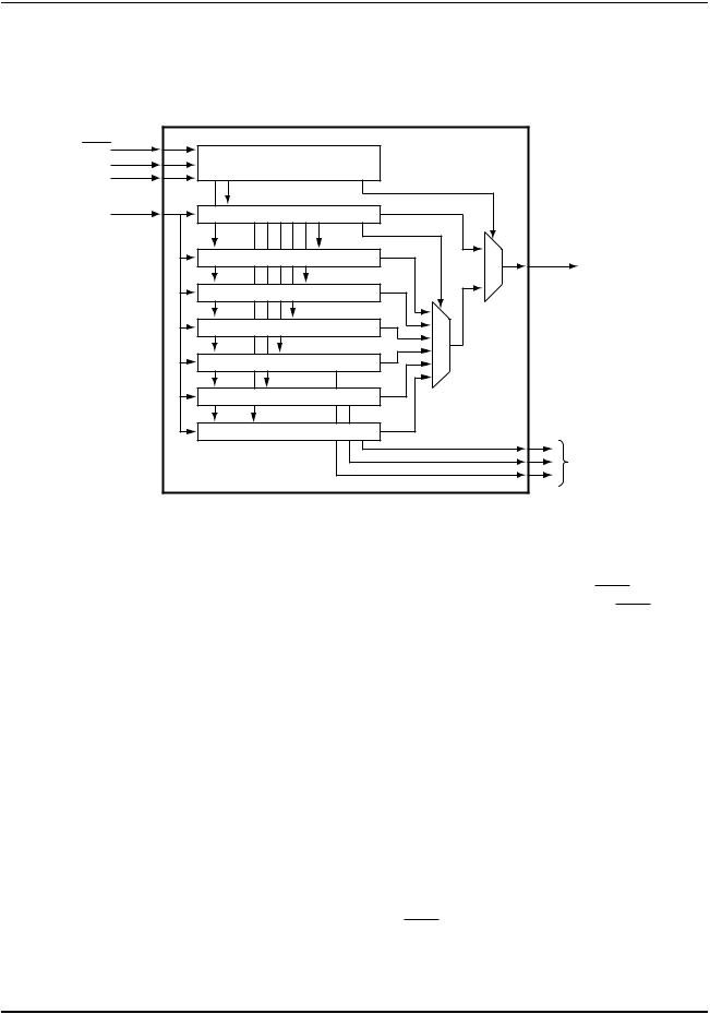
JTAG Interface
5.1Block Diagram
Figure 5-1. JTAG Module Block Diagram |
||
TRST |
TAP Controller |
|
TCK |
||
|
||
TMS |
|
|
TDI |
Instruction Register (IR) |
|
|
BYPASS Data Register |
|
|
TDO |
|
|
Boundary Scan Data Register |
|
|
IDCODE Data Register |
|
|
ABORT Data Register |
|
|
DPACC Data Register |
|
|
APACC Data Register |
|
|
Cortex-M3 |
|
|
Debug |
|
|
Port |
|
5.2Functional Description
A high-level conceptual drawing of the JTAG module is shown in Figure 5-1 on page 56. The JTAG module is composed of the Test Access Port (TAP) controller and serial shift chains with parallel update registers. The TAP controller is a simple state machine controlled by the TRST, TCK and TMS inputs. The current state of the TAP controller depends on the current value of TRST and the sequenceofvaluescapturedon TMS attherisingedgeof TCK. TheTAPcontrollerdetermineswhen the serial shift chains capture new data, shift data from TDI towards TDO, and update the parallel load registers. The current state of the TAP controller also determines whether the Instruction Register (IR) chain or one of the Data Register (DR) chains is being accessed.
The serial shift chains with parallel load registers are comprised of a single Instruction Register (IR) chain and multiple Data Register (DR) chains. The current instruction loaded in the parallel load register determines which DR chain is captured, shifted, or updated during the sequencing of the TAP controller.
Some instructions, like EXTEST and INTEST, operate on data currently in a DR chain and do not capture, shift, or update any of the chains. Instructions that are not implemented decode to the BYPASS instruction to ensure that the serial path between TDI and TDO is always connected (see Table 5-2 on page 62 for a list of implemented instructions).
See “JTAG and Boundary Scan” on page 573 for JTAG timing diagrams.
5.2.1JTAG Interface Pins
The JTAG interface consists of five standard pins: TRST,TCK, TMS, TDI, and TDO. These pins and their associated reset state are given in Table 5-1 on page 57. Detailed information on each pin follows.
56 |
November 16, 2008 |
Preliminary

LM3S6965 Microcontroller
Table 5-1. JTAG Port Pins Reset State
Pin Name |
Data Direction |
Internal Pull-Up |
InternalPull-Down |
Drive Strength |
Drive Value |
||
|
|
|
Input |
Enabled |
Disabled |
N/A |
N/A |
|
TRST |
||||||
|
TCK |
Input |
Enabled |
Disabled |
N/A |
N/A |
|
|
TMS |
Input |
Enabled |
Disabled |
N/A |
N/A |
|
|
TDI |
Input |
Enabled |
Disabled |
N/A |
N/A |
|
|
TDO |
Output |
Enabled |
Disabled |
2-mA driver |
High-Z |
|
5.2.1.1Test Reset Input (TRST)
The TRST pin is an asynchronous active Low input signal for initializing and resetting the JTAG TAP controller and associated JTAG circuitry. When TRST is asserted, the TAP controller resets to the Test-Logic-Reset state and remains there while TRST is asserted. When the TAP controller enters the Test-Logic-Reset state, the JTAG Instruction Register (IR) resets to the default instruction, IDCODE.
Bydefault,theinternalpull-upresistoronthe TRST pinisenabledafterreset. Changestothepull-up resistor settings on GPIO Port B should ensure that the internal pull-up resistor remains enabled on PB7/TRST; otherwise JTAG communication could be lost.
5.2.1.2Test Clock Input (TCK)
The TCK pin is the clock for the JTAG module. This clock is provided so the test logic can operate independently of any other system clocks. In addition, it ensures that multiple JTAG TAP controllers that are daisy-chained together can synchronously communicate serial test data between components. During normal operation, TCK is driven by a free-running clock with a nominal 50% duty cycle. When necessary, TCK can be stopped at 0 or 1 for extended periods of time. While TCK isstoppedat0or1,thestateoftheTAPcontrollerdoesnotchangeanddataintheJTAGInstruction and Data Registers is not lost.
By default, the internal pull-up resistor on the TCK pin is enabled after reset. This assures that no clocking occurs if the pin is not driven from an external source. The internal pull-up and pull-down resistors can be turned off to save internal power as long as the TCK pin is constantly being driven by an external source.
5.2.1.3Test Mode Select (TMS)
The TMS pin selects the next state of the JTAG TAP controller. TMS is sampled on the rising edge of TCK. DependingonthecurrentTAPstateandthesampledvalueof TMS,thenextstateisentered. Because the TMS pin is sampled on the rising edge of TCK, the IEEE Standard 1149.1 expects the value on TMS to change on the falling edge of TCK.
Holding TMS high for five consecutive TCK cycles drives the TAP controller state machine to the Test-Logic-Reset state. When the TAP controller enters the Test-Logic-Reset state, the JTAG Instruction Register (IR) resets to the default instruction, IDCODE. Therefore, this sequence can beusedasaresetmechanism,similartoasserting TRST. TheJTAGTestAccessPortstatemachine can be seen in its entirety in Figure 5-2 on page 59.
By default, the internal pull-up resistor on the TMS pin is enabled after reset. Changes to the pull-up resistor settings on GPIO Port C should ensure that the internal pull-up resistor remains enabled on PC1/TMS; otherwise JTAG communication could be lost.
November 16, 2008 |
57 |
Preliminary