

- •LM3S6965 Microcontroller
- •Table of Contents
- •List of Figures
- •List of Tables
- •List of Registers
- •Revision History
- •About This Document
- •Audience
- •About This Manual
- •Related Documents
- •Documentation Conventions
- •1. Architectural Overview
- •1.1. Product Features
- •1.2. Target Applications
- •1.4. Functional Overview
- •1.4.1.1. Processor Core
- •1.4.1.2. System Timer (SysTick)
- •1.4.1.3. Nested Vectored Interrupt Controller (NVIC)
- •1.4.2. Motor Control Peripherals
- •1.4.3. Analog Peripherals
- •1.4.3.2. Analog Comparators
- •1.4.4. Serial Communications Peripherals
- •1.4.4.1. UART
- •1.4.4.4. Ethernet Controller
- •1.4.5. System Peripherals
- •1.4.5.1. Programmable GPIOs
- •1.4.5.2. Four Programmable Timers
- •1.4.5.3. Watchdog Timer
- •1.4.6. Memory Peripherals
- •1.4.6.1. SRAM
- •1.4.6.2. Flash
- •1.4.7. Additional Features
- •1.4.7.1. Memory Map
- •1.4.7.2. JTAG TAP Controller
- •1.4.7.3. System Control and Clocks
- •1.4.7.4. Hibernation Module
- •1.4.8. Hardware Details
- •2.1. Block Diagram
- •2.2. Functional Description
- •2.2.1. Serial Wire and JTAG Debug
- •2.2.2. Embedded Trace Macrocell (ETM)
- •2.2.3. Trace Port Interface Unit (TPIU)
- •2.2.4. ROM Table
- •2.2.5. Memory Protection Unit (MPU)
- •2.2.6. Nested Vectored Interrupt Controller (NVIC)
- •2.2.6.1. Interrupts
- •2.2.6.2. System Timer (SysTick)
- •Functional Description
- •SysTick Control and Status Register
- •SysTick Reload Value Register
- •SysTick Current Value Register
- •SysTick Calibration Value Register
- •3. Memory Map
- •4. Interrupts
- •5. JTAG Interface
- •5.1. Block Diagram
- •5.2. Functional Description
- •5.2.1. JTAG Interface Pins
- •5.2.1.1. Test Reset Input (TRST)
- •5.2.1.2. Test Clock Input (TCK)
- •5.2.1.3. Test Mode Select (TMS)
- •5.2.1.4. Test Data Input (TDI)
- •5.2.1.5. Test Data Output (TDO)
- •5.2.2. JTAG TAP Controller
- •5.2.3. Shift Registers
- •5.2.4. Operational Considerations
- •5.2.4.1. GPIO Functionality
- •Recovering a "Locked" Device
- •5.2.4.2. ARM Serial Wire Debug (SWD)
- •JTAG-to-SWD Switching
- •SWD-to-JTAG Switching
- •5.3. Initialization and Configuration
- •5.4. Register Descriptions
- •5.4.1. Instruction Register (IR)
- •5.4.1.1. EXTEST Instruction
- •5.4.1.2. INTEST Instruction
- •5.4.1.3. SAMPLE/PRELOAD Instruction
- •5.4.1.4. ABORT Instruction
- •5.4.1.5. DPACC Instruction
- •5.4.1.6. APACC Instruction
- •5.4.1.7. IDCODE Instruction
- •5.4.1.8. BYPASS Instruction
- •5.4.2. Data Registers
- •5.4.2.1. IDCODE Data Register
- •5.4.2.2. BYPASS Data Register
- •5.4.2.3. Boundary Scan Data Register
- •5.4.2.4. APACC Data Register
- •5.4.2.5. DPACC Data Register
- •5.4.2.6. ABORT Data Register
- •6. System Control
- •6.1. Functional Description
- •6.1.1. Device Identification
- •6.1.2. Reset Control
- •6.1.2.2. Reset Sources
- •6.1.2.3. RST Pin Assertion
- •6.1.2.6. Software Reset
- •6.1.2.7. Watchdog Timer Reset
- •6.1.3. Power Control
- •6.1.4. Clock Control
- •6.1.4.1. Fundamental Clock Sources
- •6.1.4.2. Crystal Configuration for the Main Oscillator (MOSC)
- •6.1.4.3. Main PLL Frequency Configuration
- •6.1.4.4. PLL Modes
- •6.1.4.5. PLL Operation
- •6.1.5. System Control
- •6.2. Initialization and Configuration
- •6.3. Register Map
- •6.4. Register Descriptions
- •Register 1: Device Identification 0 (DID0), offset 0x000
- •Register 2: Brown-Out Reset Control (PBORCTL), offset 0x030
- •Register 3: LDO Power Control (LDOPCTL), offset 0x034
- •Register 4: Raw Interrupt Status (RIS), offset 0x050
- •Register 5: Interrupt Mask Control (IMC), offset 0x054
- •Register 6: Masked Interrupt Status and Clear (MISC), offset 0x058
- •Register 7: Reset Cause (RESC), offset 0x05C
- •Register 8: Run-Mode Clock Configuration (RCC), offset 0x060
- •Register 9: XTAL to PLL Translation (PLLCFG), offset 0x064
- •Register 10: Run-Mode Clock Configuration 2 (RCC2), offset 0x070
- •Register 11: Deep Sleep Clock Configuration (DSLPCLKCFG), offset 0x144
- •Register 12: Device Identification 1 (DID1), offset 0x004
- •Register 13: Device Capabilities 0 (DC0), offset 0x008
- •Register 14: Device Capabilities 1 (DC1), offset 0x010
- •Register 15: Device Capabilities 2 (DC2), offset 0x014
- •Register 16: Device Capabilities 3 (DC3), offset 0x018
- •Register 17: Device Capabilities 4 (DC4), offset 0x01C
- •Register 18: Run Mode Clock Gating Control Register 0 (RCGC0), offset 0x100
- •Register 19: Sleep Mode Clock Gating Control Register 0 (SCGC0), offset 0x110
- •Register 20: Deep Sleep Mode Clock Gating Control Register 0 (DCGC0), offset 0x120
- •Register 21: Run Mode Clock Gating Control Register 1 (RCGC1), offset 0x104
- •Register 22: Sleep Mode Clock Gating Control Register 1 (SCGC1), offset 0x114
- •Register 23: Deep Sleep Mode Clock Gating Control Register 1 (DCGC1), offset 0x124
- •Register 24: Run Mode Clock Gating Control Register 2 (RCGC2), offset 0x108
- •Register 25: Sleep Mode Clock Gating Control Register 2 (SCGC2), offset 0x118
- •Register 26: Deep Sleep Mode Clock Gating Control Register 2 (DCGC2), offset 0x128
- •Register 27: Software Reset Control 0 (SRCR0), offset 0x040
- •Register 28: Software Reset Control 1 (SRCR1), offset 0x044
- •Register 29: Software Reset Control 2 (SRCR2), offset 0x048
- •7. Hibernation Module
- •7.1. Block Diagram
- •7.2. Functional Description
- •7.2.1. Register Access Timing
- •7.2.2. Clock Source
- •7.2.3. Battery Management
- •7.2.6. Power Control
- •7.2.7. Initiating Hibernate
- •7.2.8. Interrupts and Status
- •7.3. Initialization and Configuration
- •7.3.1. Initialization
- •7.3.2. RTC Match Functionality (No Hibernation)
- •7.4. Register Map
- •7.5. Register Descriptions
- •Register 1: Hibernation RTC Counter (HIBRTCC), offset 0x000
- •Register 2: Hibernation RTC Match 0 (HIBRTCM0), offset 0x004
- •Register 3: Hibernation RTC Match 1 (HIBRTCM1), offset 0x008
- •Register 4: Hibernation RTC Load (HIBRTCLD), offset 0x00C
- •Register 5: Hibernation Control (HIBCTL), offset 0x010
- •Register 6: Hibernation Interrupt Mask (HIBIM), offset 0x014
- •Register 7: Hibernation Raw Interrupt Status (HIBRIS), offset 0x018
- •Register 8: Hibernation Masked Interrupt Status (HIBMIS), offset 0x01C
- •Register 9: Hibernation Interrupt Clear (HIBIC), offset 0x020
- •Register 10: Hibernation RTC Trim (HIBRTCT), offset 0x024
- •8. Internal Memory
- •8.1. Block Diagram
- •8.2. Functional Description
- •8.2.1. SRAM Memory
- •8.2.2. Flash Memory
- •8.2.2.1. Flash Memory Timing
- •8.2.2.2. Flash Memory Protection
- •8.3. Flash Memory Initialization and Configuration
- •8.3.1. Flash Programming
- •8.3.1.3. To perform a mass erase of the flash
- •8.3.2. Nonvolatile Register Programming
- •8.4. Register Map
- •8.5. Flash Register Descriptions (Flash Control Offset)
- •Register 1: Flash Memory Address (FMA), offset 0x000
- •Register 2: Flash Memory Data (FMD), offset 0x004
- •Register 3: Flash Memory Control (FMC), offset 0x008
- •Register 4: Flash Controller Raw Interrupt Status (FCRIS), offset 0x00C
- •Register 5: Flash Controller Interrupt Mask (FCIM), offset 0x010
- •Register 6: Flash Controller Masked Interrupt Status and Clear (FCMISC), offset 0x014
- •8.6. Flash Register Descriptions (System Control Offset)
- •Register 7: USec Reload (USECRL), offset 0x140
- •Register 8: Flash Memory Protection Read Enable 0 (FMPRE0), offset 0x130 and 0x200
- •Register 9: Flash Memory Protection Program Enable 0 (FMPPE0), offset 0x134 and 0x400
- •Register 10: User Debug (USER_DBG), offset 0x1D0
- •Register 11: User Register 0 (USER_REG0), offset 0x1E0
- •Register 12: User Register 1 (USER_REG1), offset 0x1E4
- •Register 13: Flash Memory Protection Read Enable 1 (FMPRE1), offset 0x204
- •Register 14: Flash Memory Protection Read Enable 2 (FMPRE2), offset 0x208
- •Register 15: Flash Memory Protection Read Enable 3 (FMPRE3), offset 0x20C
- •Register 16: Flash Memory Protection Program Enable 1 (FMPPE1), offset 0x404
- •Register 17: Flash Memory Protection Program Enable 2 (FMPPE2), offset 0x408
- •Register 18: Flash Memory Protection Program Enable 3 (FMPPE3), offset 0x40C
- •9. General-Purpose Input/Outputs (GPIOs)
- •9.1. Functional Description
- •9.1.1. Data Control
- •9.1.1.1. Data Direction Operation
- •9.1.1.2. Data Register Operation
- •9.1.2. Interrupt Control
- •9.1.3. Mode Control
- •9.1.4. Commit Control
- •9.1.5. Pad Control
- •9.1.6. Identification
- •9.2. Initialization and Configuration
- •9.3. Register Map
- •9.4. Register Descriptions
- •Register 1: GPIO Data (GPIODATA), offset 0x000
- •Register 2: GPIO Direction (GPIODIR), offset 0x400
- •Register 3: GPIO Interrupt Sense (GPIOIS), offset 0x404
- •Register 4: GPIO Interrupt Both Edges (GPIOIBE), offset 0x408
- •Register 5: GPIO Interrupt Event (GPIOIEV), offset 0x40C
- •Register 6: GPIO Interrupt Mask (GPIOIM), offset 0x410
- •Register 7: GPIO Raw Interrupt Status (GPIORIS), offset 0x414
- •Register 8: GPIO Masked Interrupt Status (GPIOMIS), offset 0x418
- •Register 9: GPIO Interrupt Clear (GPIOICR), offset 0x41C
- •Register 10: GPIO Alternate Function Select (GPIOAFSEL), offset 0x420
- •Register 11: GPIO 2-mA Drive Select (GPIODR2R), offset 0x500
- •Register 12: GPIO 4-mA Drive Select (GPIODR4R), offset 0x504
- •Register 13: GPIO 8-mA Drive Select (GPIODR8R), offset 0x508
- •Register 14: GPIO Open Drain Select (GPIOODR), offset 0x50C
- •Register 15: GPIO Pull-Up Select (GPIOPUR), offset 0x510
- •Register 16: GPIO Pull-Down Select (GPIOPDR), offset 0x514
- •Register 17: GPIO Slew Rate Control Select (GPIOSLR), offset 0x518
- •Register 18: GPIO Digital Enable (GPIODEN), offset 0x51C
- •Register 19: GPIO Lock (GPIOLOCK), offset 0x520
- •Register 20: GPIO Commit (GPIOCR), offset 0x524
- •Register 21: GPIO Peripheral Identification 4 (GPIOPeriphID4), offset 0xFD0
- •Register 22: GPIO Peripheral Identification 5 (GPIOPeriphID5), offset 0xFD4
- •Register 23: GPIO Peripheral Identification 6 (GPIOPeriphID6), offset 0xFD8
- •Register 24: GPIO Peripheral Identification 7 (GPIOPeriphID7), offset 0xFDC
- •Register 25: GPIO Peripheral Identification 0 (GPIOPeriphID0), offset 0xFE0
- •Register 26: GPIO Peripheral Identification 1 (GPIOPeriphID1), offset 0xFE4
- •Register 27: GPIO Peripheral Identification 2 (GPIOPeriphID2), offset 0xFE8
- •Register 28: GPIO Peripheral Identification 3 (GPIOPeriphID3), offset 0xFEC
- •Register 29: GPIO PrimeCell Identification 0 (GPIOPCellID0), offset 0xFF0
- •Register 30: GPIO PrimeCell Identification 1 (GPIOPCellID1), offset 0xFF4
- •Register 31: GPIO PrimeCell Identification 2 (GPIOPCellID2), offset 0xFF8
- •Register 32: GPIO PrimeCell Identification 3 (GPIOPCellID3), offset 0xFFC
- •10. General-Purpose Timers
- •10.1. Block Diagram
- •10.2. Functional Description
- •10.2.1. GPTM Reset Conditions
- •10.2.2.1. 32-Bit One-Shot/Periodic Timer Mode
- •10.2.2.2. 32-Bit Real-Time Clock Timer Mode
- •10.2.3.1. 16-Bit One-Shot/Periodic Timer Mode
- •10.2.3.3. 16-Bit Input Edge Time Mode
- •10.2.3.4. 16-Bit PWM Mode
- •10.3. Initialization and Configuration
- •10.4. Register Map
- •10.5. Register Descriptions
- •Register 1: GPTM Configuration (GPTMCFG), offset 0x000
- •Register 2: GPTM TimerA Mode (GPTMTAMR), offset 0x004
- •Register 3: GPTM TimerB Mode (GPTMTBMR), offset 0x008
- •Register 4: GPTM Control (GPTMCTL), offset 0x00C
- •Register 5: GPTM Interrupt Mask (GPTMIMR), offset 0x018
- •Register 6: GPTM Raw Interrupt Status (GPTMRIS), offset 0x01C
- •Register 7: GPTM Masked Interrupt Status (GPTMMIS), offset 0x020
- •Register 8: GPTM Interrupt Clear (GPTMICR), offset 0x024
- •Register 9: GPTM TimerA Interval Load (GPTMTAILR), offset 0x028
- •Register 10: GPTM TimerB Interval Load (GPTMTBILR), offset 0x02C
- •Register 11: GPTM TimerA Match (GPTMTAMATCHR), offset 0x030
- •Register 12: GPTM TimerB Match (GPTMTBMATCHR), offset 0x034
- •Register 13: GPTM TimerA Prescale (GPTMTAPR), offset 0x038
- •Register 14: GPTM TimerB Prescale (GPTMTBPR), offset 0x03C
- •Register 15: GPTM TimerA Prescale Match (GPTMTAPMR), offset 0x040
- •Register 16: GPTM TimerB Prescale Match (GPTMTBPMR), offset 0x044
- •Register 17: GPTM TimerA (GPTMTAR), offset 0x048
- •Register 18: GPTM TimerB (GPTMTBR), offset 0x04C
- •11. Watchdog Timer
- •11.1. Block Diagram
- •11.2. Functional Description
- •11.3. Initialization and Configuration
- •11.4. Register Map
- •11.5. Register Descriptions
- •Register 1: Watchdog Load (WDTLOAD), offset 0x000
- •Register 2: Watchdog Value (WDTVALUE), offset 0x004
- •Register 3: Watchdog Control (WDTCTL), offset 0x008
- •Register 4: Watchdog Interrupt Clear (WDTICR), offset 0x00C
- •Register 5: Watchdog Raw Interrupt Status (WDTRIS), offset 0x010
- •Register 6: Watchdog Masked Interrupt Status (WDTMIS), offset 0x014
- •Register 7: Watchdog Test (WDTTEST), offset 0x418
- •Register 8: Watchdog Lock (WDTLOCK), offset 0xC00
- •Register 10: Watchdog Peripheral Identification 5 (WDTPeriphID5), offset 0xFD4
- •Register 11: Watchdog Peripheral Identification 6 (WDTPeriphID6), offset 0xFD8
- •Register 12: Watchdog Peripheral Identification 7 (WDTPeriphID7), offset 0xFDC
- •Register 13: Watchdog Peripheral Identification 0 (WDTPeriphID0), offset 0xFE0
- •Register 14: Watchdog Peripheral Identification 1 (WDTPeriphID1), offset 0xFE4
- •Register 15: Watchdog Peripheral Identification 2 (WDTPeriphID2), offset 0xFE8
- •Register 16: Watchdog Peripheral Identification 3 (WDTPeriphID3), offset 0xFEC
- •Register 17: Watchdog PrimeCell Identification 0 (WDTPCellID0), offset 0xFF0
- •Register 18: Watchdog PrimeCell Identification 1 (WDTPCellID1), offset 0xFF4
- •Register 19: Watchdog PrimeCell Identification 2 (WDTPCellID2), offset 0xFF8
- •12. Analog-to-Digital Converter (ADC)
- •12.1. Block Diagram
- •12.2. Functional Description
- •12.2.1. Sample Sequencers
- •12.2.2. Module Control
- •12.2.2.1. Interrupts
- •12.2.2.2. Prioritization
- •12.2.2.3. Sampling Events
- •12.2.3. Hardware Sample Averaging Circuit
- •12.2.5. Differential Sampling
- •12.2.6. Test Modes
- •12.2.7. Internal Temperature Sensor
- •12.3. Initialization and Configuration
- •12.3.1. Module Initialization
- •12.3.2. Sample Sequencer Configuration
- •12.4. Register Map
- •12.5. Register Descriptions
- •Register 1: ADC Active Sample Sequencer (ADCACTSS), offset 0x000
- •Register 2: ADC Raw Interrupt Status (ADCRIS), offset 0x004
- •Register 3: ADC Interrupt Mask (ADCIM), offset 0x008
- •Register 4: ADC Interrupt Status and Clear (ADCISC), offset 0x00C
- •Register 5: ADC Overflow Status (ADCOSTAT), offset 0x010
- •Register 6: ADC Event Multiplexer Select (ADCEMUX), offset 0x014
- •Register 7: ADC Underflow Status (ADCUSTAT), offset 0x018
- •Register 8: ADC Sample Sequencer Priority (ADCSSPRI), offset 0x020
- •Register 9: ADC Processor Sample Sequence Initiate (ADCPSSI), offset 0x028
- •Register 10: ADC Sample Averaging Control (ADCSAC), offset 0x030
- •Register 12: ADC Sample Sequence Control 0 (ADCSSCTL0), offset 0x044
- •Register 16: ADC Sample Sequence Result FIFO 3 (ADCSSFIFO3), offset 0x0A8
- •Register 17: ADC Sample Sequence FIFO 0 Status (ADCSSFSTAT0), offset 0x04C
- •Register 18: ADC Sample Sequence FIFO 1 Status (ADCSSFSTAT1), offset 0x06C
- •Register 19: ADC Sample Sequence FIFO 2 Status (ADCSSFSTAT2), offset 0x08C
- •Register 20: ADC Sample Sequence FIFO 3 Status (ADCSSFSTAT3), offset 0x0AC
- •Register 21: ADC Sample Sequence Input Multiplexer Select 1 (ADCSSMUX1), offset 0x060
- •Register 22: ADC Sample Sequence Input Multiplexer Select 2 (ADCSSMUX2), offset 0x080
- •Register 23: ADC Sample Sequence Control 1 (ADCSSCTL1), offset 0x064
- •Register 24: ADC Sample Sequence Control 2 (ADCSSCTL2), offset 0x084
- •Register 25: ADC Sample Sequence Input Multiplexer Select 3 (ADCSSMUX3), offset 0x0A0
- •Register 26: ADC Sample Sequence Control 3 (ADCSSCTL3), offset 0x0A4
- •Register 27: ADC Test Mode Loopback (ADCTMLB), offset 0x100
- •13. Universal Asynchronous Receivers/Transmitters (UARTs)
- •13.1. Block Diagram
- •13.2. Functional Description
- •13.2.1. Transmit/Receive Logic
- •13.2.3. Data Transmission
- •13.2.4. Serial IR (SIR)
- •13.2.5. FIFO Operation
- •13.2.6. Interrupts
- •13.2.7. Loopback Operation
- •13.2.8. IrDA SIR block
- •13.3. Initialization and Configuration
- •13.4. Register Map
- •13.5. Register Descriptions
- •Register 1: UART Data (UARTDR), offset 0x000
- •Register 3: UART Flag (UARTFR), offset 0x018
- •Register 4: UART IrDA Low-Power Register (UARTILPR), offset 0x020
- •Register 5: UART Integer Baud-Rate Divisor (UARTIBRD), offset 0x024
- •Register 6: UART Fractional Baud-Rate Divisor (UARTFBRD), offset 0x028
- •Register 7: UART Line Control (UARTLCRH), offset 0x02C
- •Register 8: UART Control (UARTCTL), offset 0x030
- •Register 9: UART Interrupt FIFO Level Select (UARTIFLS), offset 0x034
- •Register 10: UART Interrupt Mask (UARTIM), offset 0x038
- •Register 11: UART Raw Interrupt Status (UARTRIS), offset 0x03C
- •Register 12: UART Masked Interrupt Status (UARTMIS), offset 0x040
- •Register 13: UART Interrupt Clear (UARTICR), offset 0x044
- •Register 14: UART Peripheral Identification 4 (UARTPeriphID4), offset 0xFD0
- •Register 15: UART Peripheral Identification 5 (UARTPeriphID5), offset 0xFD4
- •Register 16: UART Peripheral Identification 6 (UARTPeriphID6), offset 0xFD8
- •Register 17: UART Peripheral Identification 7 (UARTPeriphID7), offset 0xFDC
- •Register 18: UART Peripheral Identification 0 (UARTPeriphID0), offset 0xFE0
- •Register 19: UART Peripheral Identification 1 (UARTPeriphID1), offset 0xFE4
- •Register 20: UART Peripheral Identification 2 (UARTPeriphID2), offset 0xFE8
- •Register 21: UART Peripheral Identification 3 (UARTPeriphID3), offset 0xFEC
- •Register 22: UART PrimeCell Identification 0 (UARTPCellID0), offset 0xFF0
- •Register 23: UART PrimeCell Identification 1 (UARTPCellID1), offset 0xFF4
- •Register 24: UART PrimeCell Identification 2 (UARTPCellID2), offset 0xFF8
- •Register 25: UART PrimeCell Identification 3 (UARTPCellID3), offset 0xFFC
- •14. Synchronous Serial Interface (SSI)
- •14.1. Block Diagram
- •14.2. Functional Description
- •14.2.1. Bit Rate Generation
- •14.2.2. FIFO Operation
- •14.2.2.1. Transmit FIFO
- •14.2.2.2. Receive FIFO
- •14.2.3. Interrupts
- •14.2.4. Frame Formats
- •14.2.4.1. Texas Instruments Synchronous Serial Frame Format
- •14.2.4.2. Freescale SPI Frame Format
- •SPO Clock Polarity Bit
- •SPH Phase Control Bit
- •14.2.4.3. Freescale SPI Frame Format with SPO=0 and SPH=0
- •14.2.4.4. Freescale SPI Frame Format with SPO=0 and SPH=1
- •14.2.4.5. Freescale SPI Frame Format with SPO=1 and SPH=0
- •14.2.4.6. Freescale SPI Frame Format with SPO=1 and SPH=1
- •14.2.4.7. MICROWIRE Frame Format
- •14.3. Initialization and Configuration
- •14.4. Register Map
- •14.5. Register Descriptions
- •Register 1: SSI Control 0 (SSICR0), offset 0x000
- •Register 2: SSI Control 1 (SSICR1), offset 0x004
- •Register 3: SSI Data (SSIDR), offset 0x008
- •Register 4: SSI Status (SSISR), offset 0x00C
- •Register 5: SSI Clock Prescale (SSICPSR), offset 0x010
- •Register 6: SSI Interrupt Mask (SSIIM), offset 0x014
- •Register 7: SSI Raw Interrupt Status (SSIRIS), offset 0x018
- •Register 8: SSI Masked Interrupt Status (SSIMIS), offset 0x01C
- •Register 9: SSI Interrupt Clear (SSIICR), offset 0x020
- •Register 10: SSI Peripheral Identification 4 (SSIPeriphID4), offset 0xFD0
- •Register 11: SSI Peripheral Identification 5 (SSIPeriphID5), offset 0xFD4
- •Register 12: SSI Peripheral Identification 6 (SSIPeriphID6), offset 0xFD8
- •Register 13: SSI Peripheral Identification 7 (SSIPeriphID7), offset 0xFDC
- •Register 14: SSI Peripheral Identification 0 (SSIPeriphID0), offset 0xFE0
- •Register 15: SSI Peripheral Identification 1 (SSIPeriphID1), offset 0xFE4
- •Register 16: SSI Peripheral Identification 2 (SSIPeriphID2), offset 0xFE8
- •Register 17: SSI Peripheral Identification 3 (SSIPeriphID3), offset 0xFEC
- •Register 18: SSI PrimeCell Identification 0 (SSIPCellID0), offset 0xFF0
- •Register 19: SSI PrimeCell Identification 1 (SSIPCellID1), offset 0xFF4
- •Register 20: SSI PrimeCell Identification 2 (SSIPCellID2), offset 0xFF8
- •Register 21: SSI PrimeCell Identification 3 (SSIPCellID3), offset 0xFFC
- •15. Inter-Integrated Circuit (I2C) Interface
- •15.1. Block Diagram
- •15.2. Functional Description
- •15.2.1.1. START and STOP Conditions
- •15.2.1.2. Data Format with 7-Bit Address
- •15.2.1.3. Data Validity
- •15.2.1.4. Acknowledge
- •15.2.1.5. Arbitration
- •15.2.2. Available Speed Modes
- •15.2.3. Interrupts
- •15.2.3.1. I2C Master Interrupts
- •15.2.3.2. I2C Slave Interrupts
- •15.2.4. Loopback Operation
- •15.2.5. Command Sequence Flow Charts
- •15.2.5.1. I2C Master Command Sequences
- •15.2.5.2. I2C Slave Command Sequences
- •15.3. Initialization and Configuration
- •15.4. Register Map
- •Register 1: I2C Master Slave Address (I2CMSA), offset 0x000
- •Register 2: I2C Master Control/Status (I2CMCS), offset 0x004
- •Register 3: I2C Master Data (I2CMDR), offset 0x008
- •Register 4: I2C Master Timer Period (I2CMTPR), offset 0x00C
- •Register 5: I2C Master Interrupt Mask (I2CMIMR), offset 0x010
- •Register 6: I2C Master Raw Interrupt Status (I2CMRIS), offset 0x014
- •Register 7: I2C Master Masked Interrupt Status (I2CMMIS), offset 0x018
- •Register 8: I2C Master Interrupt Clear (I2CMICR), offset 0x01C
- •Register 9: I2C Master Configuration (I2CMCR), offset 0x020
- •Register 10: I2C Slave Own Address (I2CSOAR), offset 0x000
- •Register 11: I2C Slave Control/Status (I2CSCSR), offset 0x004
- •Register 12: I2C Slave Data (I2CSDR), offset 0x008
- •Register 13: I2C Slave Interrupt Mask (I2CSIMR), offset 0x00C
- •Register 14: I2C Slave Raw Interrupt Status (I2CSRIS), offset 0x010
- •Register 15: I2C Slave Masked Interrupt Status (I2CSMIS), offset 0x014
- •Register 16: I2C Slave Interrupt Clear (I2CSICR), offset 0x018
- •16. Ethernet Controller
- •16.1. Block Diagram
- •16.2. Functional Description
- •16.2.1. MAC Operation
- •16.2.1.1. Ethernet Frame Format
- •16.2.1.2. MAC Layer FIFOs
- •16.2.1.3. Ethernet Transmission Options
- •16.2.1.4. Ethernet Reception Options
- •16.2.2. Internal MII Operation
- •16.2.3. PHY Operation
- •16.2.3.1. Clock Selection
- •16.2.3.2. Auto-Negotiation
- •16.2.3.3. Polarity Correction
- •16.2.3.4. MDI/MDI-X Configuration
- •16.2.3.5. LED Indicators
- •16.2.4. Interrupts
- •16.3. Initialization and Configuration
- •16.4. Ethernet Register Map
- •16.5. Ethernet MAC Register Descriptions
- •Register 1: Ethernet MAC Raw Interrupt Status/Acknowledge (MACRIS/MACIACK), offset 0x000
- •Register 2: Ethernet MAC Interrupt Mask (MACIM), offset 0x004
- •Register 3: Ethernet MAC Receive Control (MACRCTL), offset 0x008
- •Register 4: Ethernet MAC Transmit Control (MACTCTL), offset 0x00C
- •Register 5: Ethernet MAC Data (MACDATA), offset 0x010
- •Register 6: Ethernet MAC Individual Address 0 (MACIA0), offset 0x014
- •Register 7: Ethernet MAC Individual Address 1 (MACIA1), offset 0x018
- •Register 8: Ethernet MAC Threshold (MACTHR), offset 0x01C
- •Register 9: Ethernet MAC Management Control (MACMCTL), offset 0x020
- •Register 10: Ethernet MAC Management Divider (MACMDV), offset 0x024
- •Register 11: Ethernet MAC Management Transmit Data (MACMTXD), offset 0x02C
- •Register 12: Ethernet MAC Management Receive Data (MACMRXD), offset 0x030
- •Register 13: Ethernet MAC Number of Packets (MACNP), offset 0x034
- •Register 14: Ethernet MAC Transmission Request (MACTR), offset 0x038
- •16.6. MII Management Register Descriptions
- •Register 15: Ethernet PHY Management Register 0 – Control (MR0), address 0x00
- •Register 16: Ethernet PHY Management Register 1 – Status (MR1), address 0x01
- •Register 17: Ethernet PHY Management Register 2 – PHY Identifier 1 (MR2), address 0x02
- •Register 18: Ethernet PHY Management Register 3 – PHY Identifier 2 (MR3), address 0x03
- •Register 19: Ethernet PHY Management Register 4 – Auto-Negotiation Advertisement (MR4), address 0x04
- •Register 20: Ethernet PHY Management Register 5 – Auto-Negotiation Link Partner Base Page Ability (MR5), address 0x05
- •Register 21: Ethernet PHY Management Register 6 – Auto-Negotiation Expansion (MR6), address 0x06
- •Register 23: Ethernet PHY Management Register 17 – Interrupt Control/Status (MR17), address 0x11
- •Register 24: Ethernet PHY Management Register 18 – Diagnostic (MR18), address 0x12
- •Register 25: Ethernet PHY Management Register 19 – Transceiver Control (MR19), address 0x13
- •Register 26: Ethernet PHY Management Register 23 – LED Configuration (MR23), address 0x17
- •17. Analog Comparators
- •17.1. Block Diagram
- •17.2. Functional Description
- •17.2.1. Internal Reference Programming
- •17.3. Initialization and Configuration
- •17.4. Register Map
- •17.5. Register Descriptions
- •Register 1: Analog Comparator Masked Interrupt Status (ACMIS), offset 0x000
- •Register 2: Analog Comparator Raw Interrupt Status (ACRIS), offset 0x004
- •Register 3: Analog Comparator Interrupt Enable (ACINTEN), offset 0x008
- •Register 5: Analog Comparator Status 0 (ACSTAT0), offset 0x020
- •Register 6: Analog Comparator Status 1 (ACSTAT1), offset 0x040
- •Register 7: Analog Comparator Control 0 (ACCTL0), offset 0x024
- •Register 8: Analog Comparator Control 1 (ACCTL1), offset 0x044
- •18. Pulse Width Modulator (PWM)
- •18.1. Block Diagram
- •18.2. Functional Description
- •18.2.1. PWM Timer
- •18.2.2. PWM Comparators
- •18.2.3. PWM Signal Generator
- •18.2.6. Synchronization Methods
- •18.2.7. Fault Conditions
- •18.2.8. Output Control Block
- •18.3. Initialization and Configuration
- •18.4. Register Map
- •18.5. Register Descriptions
- •Register 1: PWM Master Control (PWMCTL), offset 0x000
- •Register 2: PWM Time Base Sync (PWMSYNC), offset 0x004
- •Register 3: PWM Output Enable (PWMENABLE), offset 0x008
- •Register 4: PWM Output Inversion (PWMINVERT), offset 0x00C
- •Register 5: PWM Output Fault (PWMFAULT), offset 0x010
- •Register 6: PWM Interrupt Enable (PWMINTEN), offset 0x014
- •Register 7: PWM Raw Interrupt Status (PWMRIS), offset 0x018
- •Register 8: PWM Interrupt Status and Clear (PWMISC), offset 0x01C
- •Register 9: PWM Status (PWMSTATUS), offset 0x020
- •Register 10: PWM0 Control (PWM0CTL), offset 0x040
- •Register 11: PWM1 Control (PWM1CTL), offset 0x080
- •Register 12: PWM2 Control (PWM2CTL), offset 0x0C0
- •Register 22: PWM0 Load (PWM0LOAD), offset 0x050
- •Register 23: PWM1 Load (PWM1LOAD), offset 0x090
- •Register 24: PWM2 Load (PWM2LOAD), offset 0x0D0
- •Register 25: PWM0 Counter (PWM0COUNT), offset 0x054
- •Register 26: PWM1 Counter (PWM1COUNT), offset 0x094
- •Register 27: PWM2 Counter (PWM2COUNT), offset 0x0D4
- •Register 28: PWM0 Compare A (PWM0CMPA), offset 0x058
- •Register 29: PWM1 Compare A (PWM1CMPA), offset 0x098
- •Register 30: PWM2 Compare A (PWM2CMPA), offset 0x0D8
- •Register 31: PWM0 Compare B (PWM0CMPB), offset 0x05C
- •Register 32: PWM1 Compare B (PWM1CMPB), offset 0x09C
- •Register 33: PWM2 Compare B (PWM2CMPB), offset 0x0DC
- •Register 40: PWM0 Dead-Band Control (PWM0DBCTL), offset 0x068
- •Register 41: PWM1 Dead-Band Control (PWM1DBCTL), offset 0x0A8
- •Register 42: PWM2 Dead-Band Control (PWM2DBCTL), offset 0x0E8
- •Register 43: PWM0 Dead-Band Rising-Edge Delay (PWM0DBRISE), offset 0x06C
- •Register 44: PWM1 Dead-Band Rising-Edge Delay (PWM1DBRISE), offset 0x0AC
- •Register 45: PWM2 Dead-Band Rising-Edge Delay (PWM2DBRISE), offset 0x0EC
- •Register 46: PWM0 Dead-Band Falling-Edge-Delay (PWM0DBFALL), offset 0x070
- •Register 47: PWM1 Dead-Band Falling-Edge-Delay (PWM1DBFALL), offset 0x0B0
- •Register 48: PWM2 Dead-Band Falling-Edge-Delay (PWM2DBFALL), offset 0x0F0
- •19. Quadrature Encoder Interface (QEI)
- •19.1. Block Diagram
- •19.2. Functional Description
- •19.3. Initialization and Configuration
- •19.4. Register Map
- •19.5. Register Descriptions
- •Register 1: QEI Control (QEICTL), offset 0x000
- •Register 2: QEI Status (QEISTAT), offset 0x004
- •Register 3: QEI Position (QEIPOS), offset 0x008
- •Register 4: QEI Maximum Position (QEIMAXPOS), offset 0x00C
- •Register 5: QEI Timer Load (QEILOAD), offset 0x010
- •Register 6: QEI Timer (QEITIME), offset 0x014
- •Register 7: QEI Velocity Counter (QEICOUNT), offset 0x018
- •Register 8: QEI Velocity (QEISPEED), offset 0x01C
- •Register 9: QEI Interrupt Enable (QEIINTEN), offset 0x020
- •Register 10: QEI Raw Interrupt Status (QEIRIS), offset 0x024
- •Register 11: QEI Interrupt Status and Clear (QEIISC), offset 0x028
- •20. Pin Diagram
- •21. Signal Tables
- •22. Operating Characteristics
- •23. Electrical Characteristics
- •23.1. DC Characteristics
- •23.1.1. Maximum Ratings
- •23.1.2. Recommended DC Operating Conditions
- •23.1.4. Power Specifications
- •23.1.5. Flash Memory Characteristics
- •23.1.6. Hibernation
- •23.2. AC Characteristics
- •23.2.1. Load Conditions
- •23.2.2. Clocks
- •23.2.3. JTAG and Boundary Scan
- •23.2.4. Reset
- •23.2.5. Hibernation Module
- •23.2.8. Synchronous Serial Interface (SSI)
- •23.2.10. Ethernet Controller
- •23.2.11. Analog Comparator
- •24. Package Information
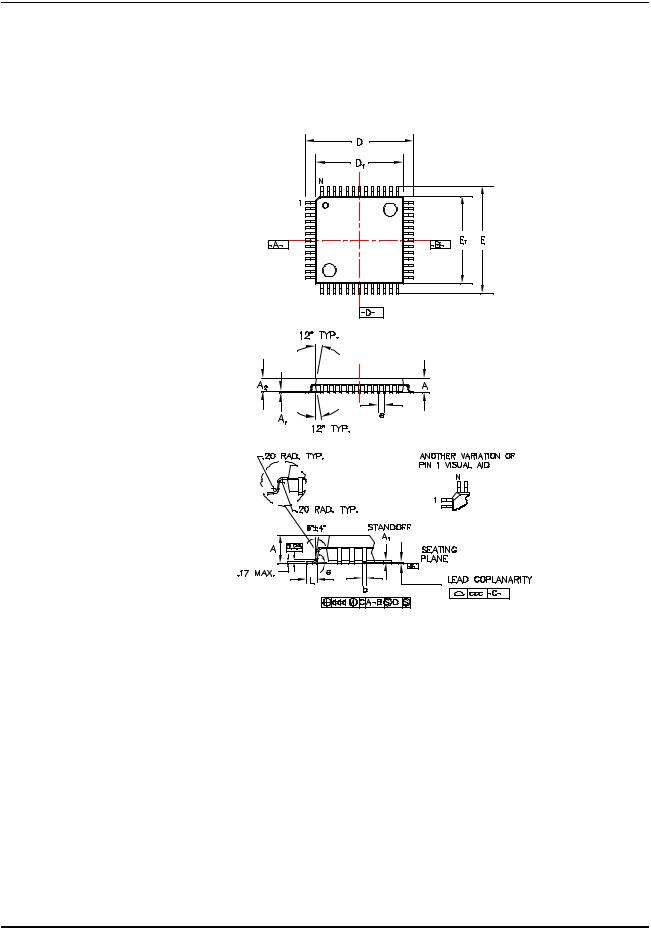
LM3S6965 Microcontroller
24 Package Information
Figure 24-1. 100-Pin LQFP Package
Note: The following notes apply to the package drawing.
1.All dimensions shown in mm.
2.Dimensions shown are nominal with tolerances indicated.
3.Foot length 'L' is measured at gage plane 0.25 mm above seating plane.
November 16, 2008 |
585 |
Preliminary

Package Information
 Body +2.00 mm Footprint, 1.4 mm package thickness
Symbols |
Leads |
100L |
A |
Max. |
1.60 |
A1 |
- |
0.05 Min./0.15 Max. |
A2 |
±0.05 |
1.40 |
D |
±0.20 |
16.00 |
D1 |
±0.05 |
14.00 |
E |
±0.20 |
16.00 |
E1 |
±0.05 |
14.00 |
L |
+0.15/-0.10 |
0.60 |
e |
Basic |
0.50 |
b |
+0.05 |
0.22 |
θ |
- |
0˚-7˚ |
ddd |
Max. |
0.08 |
ccc |
Max. |
0.08 |
JEDEC Reference Drawing |
MS-026 |
|
Variation Designator |
BED |
|
586 |
November 16, 2008 |
Preliminary
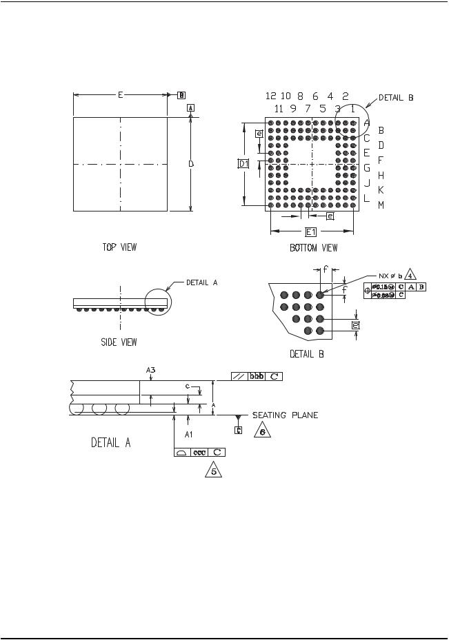
LM3S6965 Microcontroller
Figure 24-2. 108-Ball BGA Package
November 16, 2008 |
587 |
Preliminary
Package Information
 Note: The following notes apply to the package drawing.
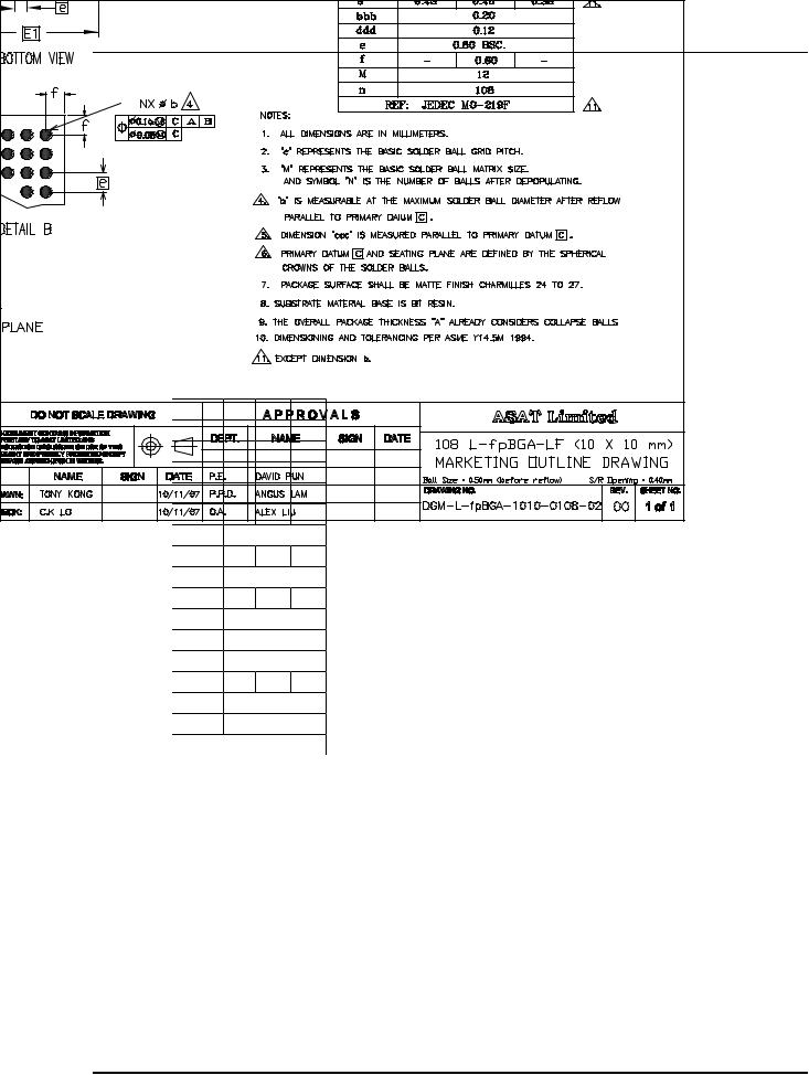
Symbols |
MIN |
NOM |
MAX |
A |
1.22 |
1.36 |
1.50 |
A1 |
0.29 |
0.34 |
0.39 |
A3 |
0.65 |
0.70 |
0.75 |
c |
0.28 |
0.32 |
0.36 |
D |
9.85 |
10.00 10.15 |
|
D1 |
8.80 BSC |
||
E |
9.85 |
10.00 10.15 |
|
E1 |
8.80 BSC |
||
b |
0.43 |
0.48 |
0.53 |
bbb |
|
.20 |
|
ddd |
|
.12 |
|
e |
0.80 BSC |
||
f |
- |
0.60 |
- |
M |
|
12 |
|
n |
|
108 |
|
REF: JEDEC MO-219F
588 |
November 16, 2008 |
|
Preliminary |

LM3S6965 Microcontroller
ASerial Flash Loader
A.1 Serial Flash Loader
The Stellaris® serial flash loader is a preprogrammed flash-resident utility used to download code to the flash memory of a device without the use of a debug interface. The serial flash loader uses a simple packet interface to provide synchronous communication with the device. The flash loader runs off the crystal and does not enable the PLL, so its speed is determined by the crystal used.
The two serial interfaces that can be used are the UART0 and SSI0 interfaces. For simplicity, both the data format and communication protocol are identical for both serial interfaces.
A.2 Interfaces
Oncecommunicationwiththeflashloaderisestablishedviaoneoftheserialinterfaces,thatinterface is used until the flash loader is reset or new code takes over. For example, once you start communicating using the SSI port, communications with the flash loader via the UART are disabled until the device is reset.
A.2.1 UART
The Universal Asynchronous Receivers/Transmitters (UART) communication uses a fixed serial format of 8 bits of data, no parity, and 1 stop bit. The baud rate used for communication is automatically detected by the flash loader and can be any valid baud rate supported by the host and the device. The auto detection sequence requires that the baud rate should be no more than 1/32 the crystal frequency of the board that is running the serial flash loader. This is actually the same as the hardware limitation for the maximum baud rate for any UART on a Stellaris® device which is calculated as follows:
Max Baud Rate = System Clock Frequency / 16
In order to determine the baud rate, the serial flash loader needs to determine the relationship between its own crystal frequency and the baud rate. This is enough information for the flash loader to configure its UART to the same baud rate as the host. This automatic baud-rate detection allows the host to use any valid baud rate that it wants to communicate with the device.
The method used to perform this automatic synchronization relies on the host sending the flash loader two bytes that are both 0x55. This generates a series of pulses to the flash loader that it can use to calculate the ratios needed to program the UART to match the host’s baud rate. After the host sends the pattern, it attempts to read back one byte of data from the UART. The flash loader returnsthevalueof0xCCtoindicatesuccessfuldetectionofthebaudrate. Ifthisbyteisnotreceived after at least twice the time required to transfer the two bytes, the host can resend another pattern of 0x55, 0x55, and wait for the 0xCC byte again until the flash loader acknowledges that it has received a synchronization pattern correctly. For example, the time to wait for data back from the flash loader should be calculated as at least 2*(20(bits/sync)/baud rate (bits/sec)). For a baud rate of 115200, this time is 2*(20/115200) or 0.35 ms.
A.2.2 SSI
The Synchronous Serial Interface (SSI) port also uses a fixed serial format for communications, with the framing defined as Motorola format with SPH set to 1 and SPO set to 1. See “Frame Formats” on page 357 in the SSI chapter for more information on formats for this transfer protocol. Like the UART, this interface has hardware requirements that limit the maximum speed that the SSI clockcanrun. ThisallowstheSSIclocktobeatmost1/12thecrystalfrequencyoftheboardrunning
November 16, 2008 |
589 |
Preliminary

Serial Flash Loader
the flash loader. Since the host device is the master, the SSI on the flash loader device does not need to determine the clock as it is provided directly by the host.
A.3 Packet Handling
All communications, with the exception of the UART auto-baud, are done via defined packets that are acknowledged (ACK) or not acknowledged (NAK) by the devices. The packets use the same format for receiving and sending packets, including the method used to acknowledge successful or unsuccessful reception of a packet.
A.3.1 Packet Format
All packets sent and received from the device use the following byte-packed format.
struct
{
unsigned char ucSize; unsigned char ucCheckSum; unsigned char Data[];
}; |
|
ucSize |
The first byte received holds the total size of the transfer including |
|
the size and checksum bytes. |
ucChecksum |
This holds a simple checksum of the bytes in the data buffer only. |
|
The algorithm is Data[0]+Data[1]+…+ Data[ucSize-3]. |
Data |
This is the raw data intended for the device, which is formatted in |
|
some form of command interface. There should be ucSize–2 |
|
bytes of data provided in this buffer to or from the device. |
A.3.2 Sending Packets
The actual bytes of the packet can be sent individually or all at once; the only limitation is that commands that cause flash memory access should limit the download sizes to prevent losing bytes during flash programming. This limitation is discussed further in the section that describes the serial flash loader command, COMMAND_SEND_DATA (see “COMMAND_SEND_DATA
(0x24)” on page 592).
Once the packet has been formatted correctly by the host, it should be sent out over the UART or SSIinterface. ThenthehostshouldpolltheUARTorSSIinterfaceforthefirstnon-zerodatareturned from the device. The first non-zero byte will either be an ACK (0xCC) or a NAK (0x33) byte from the device indicating the packet was received successfully (ACK) or unsuccessfully (NAK). This does not indicate that the actual contents of the command issued in the data portion of the packet were valid, just that the packet was received correctly.
A.3.3 Receiving Packets
Theflashloadersendsapacketofdatainthesameformatthatitreceivesapacket. Theflashloader may transfer leading zero data before the first actual byte of data is sent out. The first non-zero byte is the size of the packet followed by a checksum byte, and finally followed by the data itself. There is no break in the data after the first non-zero byte is sent from the flash loader. Once the device communicating with the flash loader receives all the bytes, it must either ACK or NAK the packet to indicate that the transmission was successful. The appropriate response after sending a NAK to the flash loader is to resend the command that failed and request the data again. If needed, the host may send leading zeros before sending down the ACK/NAK signal to the flash loader, as the
590 |
November 16, 2008 |
Preliminary
LM3S6965 Microcontroller
flash loader only accepts the first non-zero data as a valid response. This zero padding is needed by the SSI interface in order to receive data to or from the flash loader.
A.4 Commands
The next section defines the list of commands that can be sent to the flash loader. The first byte of the data should always be one of the defined commands, followed by data or parameters as determined by the command that is sent.
A.4.1 COMMAND_PING (0X20)
This command simply accepts the command and sets the global status to success. The format of the packet is as follows:
Byte[0] = 0x03;
Byte[1] = checksum(Byte[2]);
Byte[2] = COMMAND_PING;
The ping command has 3 bytes and the value for COMMAND_PING is 0x20 and the checksum of one byteisthatsamebyte,makingByte[1]also0x20. Sincethepingcommandhasnorealreturnstatus, the receipt of an ACK can be interpreted as a successful ping to the flash loader.
A.4.2 COMMAND_GET_STATUS (0x23)
This command returns the status of the last command that was issued. Typically, this command should be sent after every command to ensure that the previous command was successful or to properly respond to a failure. The command requires one byte in the data of the packet and should be followed by reading a packet with one byte of data that contains a status code. The last step is to ACK or NAK the received data so the flash loader knows that the data has been read.
Byte[0] = 0x03
Byte[1] = checksum(Byte[2])
Byte[2] = COMMAND_GET_STATUS
A.4.3 COMMAND_DOWNLOAD (0x21)
This command is sent to the flash loader to indicate where to store data and how many bytes will be sent by the COMMAND_SEND_DATA commands that follow. The command consists of two 32-bit values that are both transferred MSB first. The first 32-bit value is the address to start programming datainto,whilethesecondisthe32-bitsizeofthedatathatwillbesent. Thiscommandalsotriggers an erase of the full area to be programmed so this command takes longer than other commands. This results in a longer time to receive the ACK/NAK back from the board. This command should be followed by a COMMAND_GET_STATUS to ensure that the Program Address and Program size are valid for the device running the flash loader.
The format of the packet to send this command is a follows:
Byte[0] = 11
Byte[1] = checksum(Bytes[2:10])
Byte[2] = COMMAND_DOWNLOAD
Byte[3] = Program Address [31:24]
Byte[4] = Program Address [23:16]
Byte[5] = Program Address [15:8]
Byte[6] = Program Address [7:0]
Byte[7] = Program Size [31:24]
November 16, 2008 |
591 |
Preliminary

Serial Flash Loader
Byte[8] = Program Size [23:16]
Byte[9] = Program Size [15:8]
Byte[10] = Program Size [7:0]
A.4.4 COMMAND_SEND_DATA (0x24)
This command should only follow a COMMAND_DOWNLOAD command or another COMMAND_SEND_DATA command if more data is needed. Consecutive send data commands automatically increment address and continue programming from the previous location. The caller should limit transfers of data to a maximum 8 bytes of packet data to allow the flash to program successfully and not overflow input buffers of the serial interfaces. The command terminates programming once the number of bytes indicated by the COMMAND_DOWNLOAD command has been received. Each time this function is called it should be followed by a COMMAND_GET_STATUS to ensure that the data was successfully programmed into the flash. If the flash loader sends a NAK to this command, the flash loader does not increment the current address to allow retransmission of the previous data.
Byte[0] = 11
Byte[1] = checksum(Bytes[2:10])
Byte[2] = COMMAND_SEND_DATA
Byte[3] = Data[0]
Byte[4] = Data[1]
Byte[5] = Data[2]
Byte[6] = Data[3]
Byte[7] = Data[4]
Byte[8] = Data[5]
Byte[9] = Data[6]
Byte[10] = Data[7]
A.4.5 COMMAND_RUN (0x22)
This command is used to tell the flash loader to execute from the address passed as the parameter in this command. This command consists of a single 32-bit value that is interpreted as the address to execute. The 32-bit value is transmitted MSB first and the flash loader responds with an ACK signal back to the host device before actually executing the code at the given address. This allows the host to know that the command was received successfully and the code is now running.
Byte[0] = 7
Byte[1] = checksum(Bytes[2:6])
Byte[2] = COMMAND_RUN
Byte[3] = Execute Address[31:24]
Byte[4] = Execute Address[23:16]
Byte[5] = Execute Address[15:8]
Byte[6] = Execute Address[7:0]
A.4.6 COMMAND_RESET (0x25)
This command is used to tell the flash loader device to reset. This is useful when downloading a new image that overwrote the flash loader and wants to start from a full reset. Unlike the COMMAND_RUN command, this allows the initial stack pointer to be read by the hardware and set up for the new code. It can also be used to reset the flash loader if a critical error occurs and the host device wants to restart communication with the flash loader.
592 |
November 16, 2008 |
Preliminary

LM3S6965 Microcontroller
Byte[0] = 3
Byte[1] = checksum(Byte[2])
Byte[2] = COMMAND_RESET
The flash loader responds with an ACK signal back to the host device before actually executing the softwareresettothedevicerunningtheflashloader. Thisallowsthehosttoknowthatthecommand was received successfully and the part will be reset.
November 16, 2008 |
593 |
Preliminary
Register Quick Reference
BRegister Quick Reference
31 |
30 |
29 |
28 |
27 |
26 |
25 |
24 |
23 |
22 |
21 |
20 |
19 |
18 |
17 |
16 |
15 |
14 |
13 |
12 |
11 |
10 |
9 |
8 |
7 |
6 |
5 |
4 |
3 |
2 |
1 |
0 |
System Control
Base 0x400F.E000
DID0, type RO, offset 0x000, reset - |
|
|
|
|
|
|
|
|
|
|
|
|
VER |
|
|
|
|
|
|
|
CLASS |
|
|
|
|
|
MAJOR |
|
|
|
|
|
|
MINOR |
|
|
|
|
PBORCTL, type R/W, offset 0x030, reset 0x0000.7FFD |
|
|
|
|
|
|
|
|
|
|
|
|
|
|
|
|
|
|
|
|
|
|
|
BORIOR |
|
LDOPCTL, type R/W, offset 0x034, reset 0x0000.0000 |
|
|
|
|
|
|
|
|
|
|
|
|
|
|
|
|
|
|
|
|
|
VADJ |
|
|
|
RIS, type RO, offset 0x050, reset 0x0000.0000 |
|
|
|
|
|
|
|
|
|
|
|
|
|
|
|
|
|
|
PLLLRIS |
|
|
|
|
BORRIS |
|
IMC, type R/W, offset 0x054, reset 0x0000.0000 |
|
|
|
|
|
|
|
|
|
|
|
|
|
|
|
|
|
|
PLLLIM |
|
|
|
|
BORIM |
|
MISC, type R/W1C, offset 0x058, reset 0x0000.0000 |
|
|
|
|
|
|
|
|
|
|
|
|
|
|
|
|
|
|
PLLLMIS |
|
|
|
|
BORMIS |
|
RESC, type R/W, offset 0x05C, reset - |
|
|
|
|
|
|
|
|
|
|
|
|
|
|
|
|
|
|
|
LDO |
SW |
WDT |
BOR |
POR |
EXT |
RCC, type R/W, offset 0x060, reset 0x078E.3AD1 |
|
|
|
|
|
|
|
|
|
|
|
|
|
ACG |
|
SYSDIV |
|
USESYSDIV |
|
USEPWMDIV |
|
PWMDIV |
|
|
|
PWRDN |
BYPASS |
|
|
|
XTAL |
|
OSCSRC |
|
|
IOSCDIS |
MOSCDIS |
|
PLLCFG, type RO, offset 0x064, reset - |
|
|
|
|
|
|
|
|
|
|
|
|
|
|
|
F |
|
|
|
|
|
|
R |
|
|
RCC2, type R/W, offset 0x070, reset 0x0780.2810 |
|
|
|
|
|
|
|
|
|
|
|
|
USERCC2 |
|
SYSDIV2 |
|
|
|
|
|
|
|
|
|
|
PWRDN2 |
BYPASS2 |
|
|
|
|
|
OSCSRC2 |
|
|
|
|
|
DSLPCLKCFG, type R/W, offset 0x144, reset 0x0780.0000 |
|
|
|
|
|
|
|
|
|
|
||
|
|
DSDIVORIDE |
|
|
|
|
|
|
|
|
|
|
|
|
|
|
|
|
|
DSOSCSRC |
|
|
|
|
|
DID1, type RO, offset 0x004, reset - |
|
|
|
|
|
|
|
|
|
|
|
|
VER |
|
FAM |
|
|
|
|
PARTNO |
|
|
|
||
PINCOUNT |
|
|
|
|
|
TEMP |
|
PKG |
ROHS |
QUAL |
||
DC0, type RO, offset 0x008, reset 0x00FF.007F |
|
|
|
|
|
|
|
|
|
|
|
|
|
|
|
|
SRAMSZ |
|
|
|
|
|
|
|
|
|
|
|
|
FLASHSZ |
|
|
|
|
|
|
|
|
DC1, type RO, offset 0x010, reset 0x0011.33FF |
|
|
|
|
|
|
|
|
|
|
|
|
|
|
|
|
|
|
|
|
PWM |
|
|
|
ADC |
MINSYSDIV |
|
|
MAXADCSPD |
MPU |
HIB |
TEMPSNS |
PLL |
WDT |
SWO |
SWD |
JTAG |
|
DC2, type RO, offset 0x014, reset 0x030F.5317 |
|
|
|
|
|
|
|
|
|
|
|
|
|
|
|
COMP1 |
COMP0 |
|
|
|
TIMER3 |
TIMER2 |
TIMER1 |
TIMER0 |
|
I2C1 |
I2C0 |
|
QEI1 |
QEI0 |
|
|
|
SSI0 |
|
UART2 |
UART1 |
UART0 |
DC3, type RO, offset 0x018, reset 0x8F0F.87FF |
|
|
|
|
|
|
|
|
|
|
|
|
32KHZ |
CCP3 |
CCP2 |
CCP1 |
CCP0 |
|
|
|
|
ADC3 |
ADC2 |
ADC1 |
ADC0 |
PWMFAULT |
|
C1PLUS |
C1MINUS |
C0O |
C0PLUS |
C0MINUS |
PWM5 |
PWM4 |
PWM3 |
PWM2 |
PWM1 |
PWM0 |
594 November 16, 2008
Preliminary

LM3S6965 Microcontroller
31 |
30 |
29 |
28 |
27 |
26 |
25 |
24 |
23 |
22 |
21 |
20 |
19 |
18 |
17 |
16 |
15 |
14 |
13 |
12 |
11 |
10 |
9 |
8 |
7 |
6 |
5 |
4 |
3 |
2 |
1 |
0 |
DC4, type RO, offset 0x01C, reset 0x5000.007F |
|
|
|
|
|
|
|
|
|
|
|
||||
|
EPHY0 |
|
EMAC0 |
|
|
|
|
|
|
|
|
|
|
|
|
|
|
|
|
|
|
|
|
|
GPIOG |
GPIOF |
GPIOE |
GPIOD |
GPIOC |
GPIOB |
GPIOA |
RCGC0, type R/W, offset 0x100, reset 0x00000040 |
|
|
|
|
|
|
|
|
|
|
|
||||
|
|
|
|
|
|
|
|
|
|
|
PWM |
|
|
|
ADC |
|
|
|
|
|
|
MAXADCSPD |
|
HIB |
|
|
WDT |
|
|
|
|
SCGC0, type R/W, offset 0x110, reset 0x00000040 |
|
|
|
|
|
|
|
|
|
|
|
||||
|
|
|
|
|
|
|
|
|
|
|
PWM |
|
|
|
ADC |
|
|
|
|
|
|
MAXADCSPD |
|
HIB |
|
|
WDT |
|
|
|
|
DCGC0, type R/W, offset 0x120, reset 0x00000040 |
|
|
|
|
|
|
|
|
|
|
|
||||
|
|
|
|
|
|
|
|
|
|
|
PWM |
|
|
|
ADC |
|
|
|
|
|
|
MAXADCSPD |
|
HIB |
|
|
WDT |
|
|
|
|
RCGC1, type R/W, offset 0x104, reset 0x00000000 |
|
|
|
|
|
|
|
|
|
|
|
||||
|
|
|
|
|
|
COMP1 |
COMP0 |
|
|
|
|
TIMER3 |
TIMER2 |
TIMER1 |
TIMER0 |
|
I2C1 |
|
I2C0 |
|
|
QEI1 |
QEI0 |
|
|
|
SSI0 |
|
UART2 |
UART1 |
UART0 |
SCGC1, type R/W, offset 0x114, reset 0x00000000 |
|
|
|
|
|
|
|
|
|
|
|
||||
|
|
|
|
|
|
COMP1 |
COMP0 |
|
|
|
|
TIMER3 |
TIMER2 |
TIMER1 |
TIMER0 |
|
I2C1 |
|
I2C0 |
|
|
QEI1 |
QEI0 |
|
|
|
SSI0 |
|
UART2 |
UART1 |
UART0 |
DCGC1, type R/W, offset 0x124, reset 0x00000000 |
|
|
|
|
|
|
|
|
|
|
|
||||
|
|
|
|
|
|
COMP1 |
COMP0 |
|
|
|
|
TIMER3 |
TIMER2 |
TIMER1 |
TIMER0 |
|
I2C1 |
|
I2C0 |
|
|
QEI1 |
QEI0 |
|
|
|
SSI0 |
|
UART2 |
UART1 |
UART0 |
RCGC2, type R/W, offset 0x108, reset 0x00000000 |
|
|
|
|
|
|
|
|
|
|
|
||||
|
EPHY0 |
|
EMAC0 |
|
|
|
|
|
|
|
|
|
|
|
|
|
|
|
|
|
|
|
|
|
GPIOG |
GPIOF |
GPIOE |
GPIOD |
GPIOC |
GPIOB |
GPIOA |
SCGC2, type R/W, offset 0x118, reset 0x00000000 |
|
|
|
|
|
|
|
|
|
|
|
||||
|
EPHY0 |
|
EMAC0 |
|
|
|
|
|
|
|
|
|
|
|
|
|
|
|
|
|
|
|
|
|
GPIOG |
GPIOF |
GPIOE |
GPIOD |
GPIOC |
GPIOB |
GPIOA |
DCGC2, type R/W, offset 0x128, reset 0x00000000 |
|
|
|
|
|
|
|
|
|
|
|
||||
|
EPHY0 |
|
EMAC0 |
|
|
|
|
|
|
|
|
|
|
|
|
|
|
|
|
|
|
|
|
|
GPIOG |
GPIOF |
GPIOE |
GPIOD |
GPIOC |
GPIOB |
GPIOA |
SRCR0, type R/W, offset 0x040, reset 0x00000000 |
|
|
|
|
|
|
|
|
|
|
|
||||
|
|
|
|
|
|
|
|
|
|
|
PWM |
|
|
|
ADC |
|
|
|
|
|
|
|
|
|
HIB |
|
|
WDT |
|
|
|
SRCR1, type R/W, offset 0x044, reset 0x00000000 |
|
|
|
|
|
|
|
|
|
|
|
||||
|
|
|
|
|
|
COMP1 |
COMP0 |
|
|
|
|
TIMER3 |
TIMER2 |
TIMER1 |
TIMER0 |
|
I2C1 |
|
I2C0 |
|
|
QEI1 |
QEI0 |
|
|
|
SSI0 |
|
UART2 |
UART1 |
UART0 |
SRCR2, type R/W, offset 0x048, reset 0x00000000 |
|
|
|
|
|
|
|
|
|
|
|
||||
|
EPHY0 |
|
EMAC0 |
|
|
|
|
|
|
|
|
|
|
|
|
|
|
|
|
|
|
|
|
|
GPIOG |
GPIOF |
GPIOE |
GPIOD |
GPIOC |
GPIOB |
GPIOA |
Hibernation Module
Base 0x400F.C000
 HIBRTCC, type RO, offset 0x000, reset 0x0000.0000
RTCC
RTCC
 HIBRTCM0, type R/W, offset 0x004, reset 0xFFFF.FFFF
RTCM0
RTCM0
 HIBRTCM1, type R/W, offset 0x008, reset 0xFFFF.FFFF
RTCM1
RTCM1
 HIBRTCLD, type R/W, offset 0x00C, reset 0xFFFF.FFFF
RTCLD
RTCLD
November 16, 2008 |
595 |
Preliminary

Register Quick Reference
31 |
30 |
29 |
28 |
27 |
26 |
25 |
24 |
23 |
22 |
21 |
20 |
19 |
18 |
17 |
16 |
15 |
14 |
13 |
12 |
11 |
10 |
9 |
8 |
7 |
6 |
5 |
4 |
3 |
2 |
1 |
0 |
HIBCTL, type R/W, offset 0x010, reset 0x0000.0000 |
|
|
|
|
|
|
|
|
|
|
|
||||
|
|
|
|
|
|
|
|
VABORT |
CLK32EN LOWBATEN |
PINWEN |
RTCWEN |
CLKSEL |
HIBREQ |
RTCEN |
|
HIBIM, type R/W, offset 0x014, reset 0x0000.0000 |
|
|
|
|
|
|
|
|
|
|
|
||||
|
|
|
|
|
|
|
|
|
|
|
|
EXTW |
LOWBAT |
RTCALT1 RTCALT0 |
|
HIBRIS, type RO, offset 0x018, reset 0x0000.0000 |
|
|
|
|
|
|
|
|
|
|
|
||||
|
|
|
|
|
|
|
|
|
|
|
|
EXTW |
LOWBAT |
RTCALT1 RTCALT0 |
|
HIBMIS, type RO, offset 0x01C, reset 0x0000.0000 |
|
|
|
|
|
|
|
|
|
|
|
||||
|
|
|
|
|
|
|
|
|
|
|
|
EXTW |
LOWBAT |
RTCALT1 RTCALT0 |
|
HIBIC, type R/W1C, offset 0x020, reset 0x0000.0000 |
|
|
|
|
|
|
|
|
|
|
|
||||
|
|
|
|
|
|
|
|
|
|
|
|
EXTW |
LOWBAT |
RTCALT1 RTCALT0 |
|
HIBRTCT, type R/W, offset 0x024, reset 0x0000.7FFF |
|
|
|
|
|
|
|
|
|
|
|
||||
TRIM
 HIBDATA, type R/W, offset 0x030-0x12C, reset 0x0000.0000
RTD
RTD
Internal Memory
Flash Registers (Flash Control Offset)
Base 0x400F.D000
 FMA, type R/W, offset 0x000, reset 0x0000.0000
OFFSET
OFFSET
 FMD, type R/W, offset 0x004, reset 0x0000.0000
DATA
DATA
 FMC, type R/W, offset 0x008, reset 0x0000.0000
WRKEY


 COMT
COMT  MERASE
  ERASE
ERASE  WRITE
WRITE 
FCRIS, type RO, offset 0x00C, reset 0x0000.0000
PRIS  ARIS
ARIS
FCIM, type R/W, offset 0x010, reset 0x0000.0000


 PMASK
PMASK  AMASK
AMASK 
FCMISC, type R/W1C, offset 0x014, reset 0x0000.0000


 PMISC
PMISC  AMISC
AMISC 
Internal Memory
Flash Registers (System Control Offset)
Base 0x400F.E000
 USECRL, type R/W, offset 0x140, reset 0x31
USEC
 FMPRE0, type R/W, offset 0x130 and 0x200, reset 0xFFFF.FFFF
READ_ENABLE
READ_ENABLE
596 |
November 16, 2008 |
Preliminary

LM3S6965 Microcontroller
31 |
30 |
29 |
28 |
27 |
26 |
25 |
24 |
23 |
22 |
21 |
20 |
19 |
18 |
17 |
16 |
15 |
14 |
13 |
12 |
11 |
10 |
9 |
8 |
7 |
6 |
5 |
4 |
3 |
2 |
1 |
0 |
FMPPE0, type R/W, offset 0x134 and 0x400, reset 0xFFFF.FFFF |
|
|
|
|
|
|
|
|
|
|
|||||
|
|
|
|
|
|
|
PROG_ENABLE |
|
|
|
|
|
|
|
|
|
|
|
|
|
|
|
PROG_ENABLE |
|
|
|
|
|
|
|
|
USER_DBG, type R/W, offset 0x1D0, reset 0xFFFF.FFFE |
|
|
|
|
|
|
|
|
|
|
|
||||
NW |
|
|
|
|
|
|
|
DATA |
|
|
|
|
|
|
|
|
|
|
|
|
|
DATA |
|
|
|
|
|
|
|
DBG1 |
DBG0 |
USER_REG0, type R/W, offset 0x1E0, reset 0xFFFF.FFFF |
|
|
|
|
|
|
|
|
|
|
|
||||
NW |
|
|
|
|
|
|
|
DATA |
|
|
|
|
|
|
|
|
|
|
|
|
|
|
|
DATA |
|
|
|
|
|
|
|
USER_REG1, type R/W, offset 0x1E4, reset 0xFFFF.FFFF |
|
|
|
|
|
|
|
|
|
|
|
||||
NW |
|
|
|
|
|
|
|
DATA |
|
|
|
|
|
|
|
DATA
 FMPRE1, type R/W, offset 0x204, reset 0xFFFF.FFFF
READ_ENABLE
READ_ENABLE
 FMPRE2, type R/W, offset 0x208, reset 0xFFFF.FFFF
READ_ENABLE
READ_ENABLE
 FMPRE3, type R/W, offset 0x20C, reset 0xFFFF.FFFF
READ_ENABLE
READ_ENABLE
 FMPPE1, type R/W, offset 0x404, reset 0xFFFF.FFFF
PROG_ENABLE
PROG_ENABLE
 FMPPE2, type R/W, offset 0x408, reset 0xFFFF.FFFF
PROG_ENABLE
PROG_ENABLE
 FMPPE3, type R/W, offset 0x40C, reset 0xFFFF.FFFF
PROG_ENABLE
PROG_ENABLE
General-Purpose Input/Outputs (GPIOs)
GPIO Port A base: 0x4000.4000
GPIO Port B base: 0x4000.5000
GPIO Port C base: 0x4000.6000
GPIO Port D base: 0x4000.7000
GPIO Port E base: 0x4002.4000
GPIO Port F base: 0x4002.5000
GPIO Port G base: 0x4002.6000
 GPIODATA, type R/W, offset 0x000, reset 0x0000.0000
DATA
 GPIODIR, type R/W, offset 0x400, reset 0x0000.0000
DIR
 GPIOIS, type R/W, offset 0x404, reset 0x0000.0000
IS
 GPIOIBE, type R/W, offset 0x408, reset 0x0000.0000
IBE
 GPIOIEV, type R/W, offset 0x40C, reset 0x0000.0000
IEV
November 16, 2008 |
597 |
Preliminary

Register Quick Reference
31 |
30 |
29 |
28 |
27 |
26 |
25 |
24 |
23 |
22 |
21 |
20 |
19 |
18 |
17 |
16 |
15 |
14 |
13 |
12 |
11 |
10 |
9 |
8 |
7 |
6 |
5 |
4 |
3 |
2 |
1 |
0 |
 GPIOIM, type R/W, offset 0x410, reset 0x0000.0000
IME
 GPIORIS, type RO, offset 0x414, reset 0x0000.0000
RIS
 GPIOMIS, type RO, offset 0x418, reset 0x0000.0000
MIS
 GPIOICR, type W1C, offset 0x41C, reset 0x0000.0000
IC
 GPIOAFSEL, type R/W, offset 0x420, reset -
AFSEL
 GPIODR2R, type R/W, offset 0x500, reset 0x0000.00FF
DRV2
 GPIODR4R, type R/W, offset 0x504, reset 0x0000.0000
DRV4
 GPIODR8R, type R/W, offset 0x508, reset 0x0000.0000
DRV8
 GPIOODR, type R/W, offset 0x50C, reset 0x0000.0000
ODE
 GPIOPUR, type R/W, offset 0x510, reset -
PUE
 GPIOPDR, type R/W, offset 0x514, reset 0x0000.0000
PDE
 GPIOSLR, type R/W, offset 0x518, reset 0x0000.0000
SRL
 GPIODEN, type R/W, offset 0x51C, reset -
DEN
 GPIOLOCK, type R/W, offset 0x520, reset 0x0000.0001
LOCK
LOCK
 GPIOCR, type -, offset 0x524, reset -
CR
 GPIOPeriphID4, type RO, offset 0xFD0, reset 0x0000.0000
PID4
 GPIOPeriphID5, type RO, offset 0xFD4, reset 0x0000.0000
PID5
598 |
November 16, 2008 |
Preliminary
LM3S6965 Microcontroller
31 |
30 |
29 |
28 |
27 |
26 |
25 |
24 |
23 |
22 |
21 |
20 |
19 |
18 |
17 |
16 |
15 |
14 |
13 |
12 |
11 |
10 |
9 |
8 |
7 |
6 |
5 |
4 |
3 |
2 |
1 |
0 |
 GPIOPeriphID6, type RO, offset 0xFD8, reset 0x0000.0000
PID6
 GPIOPeriphID7, type RO, offset 0xFDC, reset 0x0000.0000
PID7
 GPIOPeriphID0, type RO, offset 0xFE0, reset 0x0000.0061
PID0
 GPIOPeriphID1, type RO, offset 0xFE4, reset 0x0000.0000
PID1
 GPIOPeriphID2, type RO, offset 0xFE8, reset 0x0000.0018
PID2
 GPIOPeriphID3, type RO, offset 0xFEC, reset 0x0000.0001
PID3
 GPIOPCellID0, type RO, offset 0xFF0, reset 0x0000.000D
CID0
 GPIOPCellID1, type RO, offset 0xFF4, reset 0x0000.00F0
CID1
 GPIOPCellID2, type RO, offset 0xFF8, reset 0x0000.0005
CID2
 GPIOPCellID3, type RO, offset 0xFFC, reset 0x0000.00B1
CID3
General-Purpose Timers
Timer0 base: 0x4003.0000
Timer1 base: 0x4003.1000
Timer2 base: 0x4003.2000
Timer3 base: 0x4003.3000
 GPTMCFG, type R/W, offset 0x000, reset 0x0000.0000
|
|
|
|
|
|
GPTMCFG |
GPTMTAMR, type R/W, offset 0x004, reset 0x0000.0000 |
|
|
|
|
|
|
|
|
|
|
TAAMS |
TACMR |
TAMR |
GPTMTBMR, type R/W, offset 0x008, reset 0x0000.0000 |
|
|
|
|
|
|
|
|
|
|
TBAMS |
TBCMR |
TBMR |
GPTMCTL, type R/W, offset 0x00C, reset 0x0000.0000 |
|
|
|
|
|
|
TBPWML TBOTE |
TBEVENT |
TBSTALL TBEN |
TAPWML TAOTE RTCEN |
TAEVENT |
TASTALL TAEN |
|
GPTMIMR, type R/W, offset 0x018, reset 0x0000.0000 |
|
|
|
|
|
|


 CBEIM
CBEIM  CBMIM
CBMIM  TBTOIM


 RTCIM
RTCIM  CAEIM
CAEIM  CAMIM
CAMIM  TATOIM
GPTMRIS, type RO, offset 0x01C, reset 0x0000.0000


 CBERIS
  CBMRIS
  TBTORIS


 RTCRIS
  CAERIS
  CAMRIS
  TATORIS
November 16, 2008 |
599 |
Preliminary
Register Quick Reference
31 |
30 |
29 |
28 |
27 |
26 |
25 |
24 |
23 |
22 |
21 |
20 |
19 |
18 |
17 |
16 |
15 |
14 |
13 |
12 |
11 |
10 |
9 |
8 |
7 |
6 |
5 |
4 |
3 |
2 |
1 |
0 |
 GPTMMIS, type RO, offset 0x020, reset 0x0000.0000


 CBEMIS
  CBMMIS
  TBTOMIS


 RTCMIS
  CAEMIS
  CAMMIS
  TATOMIS
GPTMICR, type W1C, offset 0x024, reset 0x0000.0000


 CBECINT
 CBMCINT
 TBTOCINT


 RTCCINT
 CAECINT
 CAMCINT
 TATOCINT
GPTMTAILR, type R/W, offset 0x028, reset 0x0000.FFFF (16-bit mode) and 0xFFFF.FFFF (32-bit mode)
TAILRH
TAILRL
 GPTMTBILR, type R/W, offset 0x02C, reset 0x0000.FFFF
TBILRL
 GPTMTAMATCHR, type R/W, offset 0x030, reset 0x0000.FFFF (16-bit mode) and 0xFFFF.FFFF (32-bit mode)
TAMRH
TAMRL
 GPTMTBMATCHR, type R/W, offset 0x034, reset 0x0000.FFFF
TBMRL
 GPTMTAPR, type R/W, offset 0x038, reset 0x0000.0000
TAPSR
 GPTMTBPR, type R/W, offset 0x03C, reset 0x0000.0000
TBPSR
 GPTMTAPMR, type R/W, offset 0x040, reset 0x0000.0000
TAPSMR
 GPTMTBPMR, type R/W, offset 0x044, reset 0x0000.0000
TBPSMR
 GPTMTAR, type RO, offset 0x048, reset 0x0000.FFFF (16-bit mode) and 0xFFFF.FFFF (32-bit mode)
TARH TARL
 GPTMTBR, type RO, offset 0x04C, reset 0x0000.FFFF
TBRL
Watchdog Timer
Base 0x4000.0000
 WDTLOAD, type R/W, offset 0x000, reset 0xFFFF.FFFF
WDTLoad
WDTLoad
 WDTVALUE, type RO, offset 0x004, reset 0xFFFF.FFFF
WDTValue
WDTValue
 WDTCTL, type R/W, offset 0x008, reset 0x0000.0000


 RESEN
RESEN  INTEN
INTEN 
WDTICR, type WO, offset 0x00C, reset -
WDTIntClr
WDTIntClr
 WDTRIS, type RO, offset 0x010, reset 0x0000.0000


 WDTRIS
600 |
November 16, 2008 |
Preliminary
LM3S6965 Microcontroller
31 |
30 |
29 |
28 |
27 |
26 |
25 |
24 |
23 |
22 |
21 |
20 |
19 |
18 |
17 |
16 |
15 |
14 |
13 |
12 |
11 |
10 |
9 |
8 |
7 |
6 |
5 |
4 |
3 |
2 |
1 |
0 |
 WDTMIS, type RO, offset 0x014, reset 0x0000.0000


 WDTMIS
WDTTEST, type R/W, offset 0x418, reset 0x0000.0000


 STALL
STALL 


WDTLOCK, type R/W, offset 0xC00, reset 0x0000.0000
WDTLock
WDTLock
 WDTPeriphID4, type RO, offset 0xFD0, reset 0x0000.0000
PID4
 WDTPeriphID5, type RO, offset 0xFD4, reset 0x0000.0000
PID5
 WDTPeriphID6, type RO, offset 0xFD8, reset 0x0000.0000
PID6
 WDTPeriphID7, type RO, offset 0xFDC, reset 0x0000.0000
PID7
 WDTPeriphID0, type RO, offset 0xFE0, reset 0x0000.0005
PID0
 WDTPeriphID1, type RO, offset 0xFE4, reset 0x0000.0018
PID1
 WDTPeriphID2, type RO, offset 0xFE8, reset 0x0000.0018
PID2
 WDTPeriphID3, type RO, offset 0xFEC, reset 0x0000.0001
PID3
 WDTPCellID0, type RO, offset 0xFF0, reset 0x0000.000D
CID0
 WDTPCellID1, type RO, offset 0xFF4, reset 0x0000.00F0
CID1
 WDTPCellID2, type RO, offset 0xFF8, reset 0x0000.0005
CID2
 WDTPCellID3, type RO, offset 0xFFC, reset 0x0000.00B1
CID3
Analog-to-Digital Converter (ADC)
Base 0x4003.8000
 ADCACTSS, type R/W, offset 0x000, reset 0x0000.0000


 ASEN3
ASEN3  ASEN2
ASEN2  ASEN1
ASEN1  ASEN0
ASEN0 
ADCRIS, type RO, offset 0x004, reset 0x0000.0000
INR3  INR2
INR2  INR1
INR1  INR0
INR0
November 16, 2008 |
601 |
Preliminary

Register Quick Reference
31 |
30 |
29 |
28 |
27 |
26 |
25 |
24 |
23 |
22 |
21 |
20 |
19 |
18 |
17 |
16 |
15 |
14 |
13 |
12 |
11 |
10 |
9 |
8 |
7 |
6 |
5 |
4 |
3 |
2 |
1 |
0 |
ADCIM, type R/W, offset 0x008, reset 0x0000.0000 |
|
|
|
|
|
|
|
|
|
|
|
||||
|
|
|
|
|
|
|
|
|
|
|
|
MASK3 |
MASK2 |
MASK1 |
MASK0 |
ADCISC, type R/W1C, offset 0x00C, reset 0x0000.0000 |
|
|
|
|
|
|
|
|
|
|
|
||||
|
|
|
|
|
|
|
|
|
|
|
|
IN3 |
IN2 |
IN1 |
IN0 |
ADCOSTAT, type R/W1C, offset 0x010, reset 0x0000.0000 |
|
|
|
|
|
|
|
|
|
|
|||||
|
|
|
|
|
|
|
|
|
|
|
|
OV3 |
OV2 |
OV1 |
OV0 |
ADCEMUX, type R/W, offset 0x014, reset 0x0000.0000 |
|
|
|
|
|
|
|
|
|
|
|
||||
|
|
EM3 |
|
|
|
EM2 |
|
|
|
EM1 |
|
|
EM0 |
|
|
ADCUSTAT, type R/W1C, offset 0x018, reset 0x0000.0000 |
|
|
|
|
|
|
|
|
|
|
|
||||
|
|
|
|
|
|
|
|
|
|
|
|
UV3 |
UV2 |
UV1 |
UV0 |
ADCSSPRI, type R/W, offset 0x020, reset 0x0000.3210 |
|
|
|
|
|
|
|
|
|
|
|
||||
|
|
|
SS3 |
|
|
|
SS2 |
|
|
SS1 |
|
|
|
SS0 |
|
ADCPSSI, type WO, offset 0x028, reset - |
|
|
|
|
|
|
|
|
|
|
|
|
|||
|
|
|
|
|
|
|
|
|
|
|
|
SS3 |
SS2 |
SS1 |
SS0 |
ADCSAC, type R/W, offset 0x030, reset 0x0000.0000 |
|
|
|
|
|
|
|
|
|
|
|
||||
|
|
|
|
|
|
|
|
|
|
|
|
|
|
AVG |
|
ADCSSMUX0, type R/W, offset 0x040, reset 0x0000.0000 |
|
|
|
|
|
|
|
|
|
|
|
||||
|
|
MUX7 |
|
|
MUX6 |
|
|
MUX5 |
|
|
|
MUX4 |
|||
|
|
MUX3 |
|
|
MUX2 |
|
|
MUX1 |
|
|
|
MUX0 |
|||
ADCSSCTL0, type R/W, offset 0x044, reset 0x0000.0000 |
|
|
|
|
|
|
|
|
|
|
|
||||
TS7 |
IE7 |
END7 |
D7 |
TS6 |
IE6 |
END6 |
D6 |
TS5 |
IE5 |
END5 |
D5 |
TS4 |
IE4 |
END4 |
D4 |
TS3 |
IE3 |
END3 |
D3 |
TS2 |
IE2 |
END2 |
D2 |
TS1 |
IE1 |
END1 |
D1 |
TS0 |
IE0 |
END0 |
D0 |
ADCSSFIFO0, type RO, offset 0x048, reset 0x0000.0000 |
|
|
|
|
|
|
|
|
|
|
|
||||
|
|
|
|
|
|
|
|
|
|
DATA |
|
|
|
|
|
ADCSSFIFO1, type RO, offset 0x068, reset 0x0000.0000 |
|
|
|
|
|
|
|
|
|
|
|
||||
|
|
|
|
|
|
|
|
|
|
DATA |
|
|
|
|
|
ADCSSFIFO2, type RO, offset 0x088, reset 0x0000.0000 |
|
|
|
|
|
|
|
|
|
|
|
||||
|
|
|
|
|
|
|
|
|
|
DATA |
|
|
|
|
|
ADCSSFIFO3, type RO, offset 0x0A8, reset 0x0000.0000 |
|
|
|
|
|
|
|
|
|
|
|
||||
|
|
|
|
|
|
|
|
|
|
DATA |
|
|
|
|
|
ADCSSFSTAT0, type RO, offset 0x04C, reset 0x0000.0100 |
|
|
|
|
|
|
|
|
|
|
|||||
|
|
|
FULL |
|
|
|
EMPTY |
|
|
HPTR |
|
|
TPTR |
|
|
ADCSSFSTAT1, type RO, offset 0x06C, reset 0x0000.0100 |
|
|
|
|
|
|
|
|
|
|
|||||
|
|
|
FULL |
|
|
|
EMPTY |
|
|
HPTR |
|
|
TPTR |
|
|
ADCSSFSTAT2, type RO, offset 0x08C, reset 0x0000.0100 |
|
|
|
|
|
|
|
|
|
|
|||||
|
|
|
FULL |
|
|
|
EMPTY |
|
|
HPTR |
|
|
TPTR |
|
|
602 |
November 16, 2008 |
Preliminary

LM3S6965 Microcontroller
31 |
30 |
29 |
28 |
27 |
26 |
25 |
24 |
23 |
22 |
21 |
20 |
19 |
18 |
17 |
16 |
15 |
14 |
13 |
12 |
11 |
10 |
9 |
8 |
7 |
6 |
5 |
4 |
3 |
2 |
1 |
0 |
ADCSSFSTAT3, type RO, offset 0x0AC, reset 0x0000.0100 |
|
|
|
|
|
|
|
|
|
|
|||||
|
|
FULL |
|
|
EMPTY |
|
|
HPTR |
|
|
|
TPTR |
|
||
ADCSSMUX1, type R/W, offset 0x060, reset 0x0000.0000 |
|
|
|
|
|
|
|
|
|
|
|
||||
|
|
MUX3 |
|
|
|
MUX2 |
|
|
|
MUX1 |
|
|
|
MUX0 |
|
ADCSSMUX2, type R/W, offset 0x080, reset 0x0000.0000 |
|
|
|
|
|
|
|
|
|
|
|
||||
|
|
MUX3 |
|
|
|
MUX2 |
|
|
|
MUX1 |
|
|
|
MUX0 |
|
ADCSSCTL1, type R/W, offset 0x064, reset 0x0000.0000 |
|
|
|
|
|
|
|
|
|
|
|
||||
TS3 |
IE3 |
END3 |
D3 |
TS2 |
IE2 |
END2 |
D2 |
TS1 |
IE1 |
END1 |
D1 |
TS0 |
IE0 |
END0 |
D0 |
ADCSSCTL2, type R/W, offset 0x084, reset 0x0000.0000 |
|
|
|
|
|
|
|
|
|
|
|
||||
TS3 |
IE3 |
END3 |
D3 |
TS2 |
IE2 |
END2 |
D2 |
TS1 |
IE1 |
END1 |
D1 |
TS0 |
IE0 |
END0 |
D0 |
ADCSSMUX3, type R/W, offset 0x0A0, reset 0x0000.0000 |
|
|
|
|
|
|
|
|
|
|
|
||||
|
|
|
|
|
|
|
|
|
|
|
|
|
|
MUX0 |
|
ADCSSCTL3, type R/W, offset 0x0A4, reset 0x0000.0002 |
|
|
|
|
|
|
|
|
|
|
|
||||
|
|
|
|
|
|
|
|
|
|
|
|
TS0 |
IE0 |
END0 |
D0 |
ADCTMLB, type R/W, offset 0x100, reset 0x0000.0000 |
|
|
|
|
|
|
|
|
|
|
|
||||
LB
Universal Asynchronous Receivers/Transmitters (UARTs)
UART0 base: 0x4000.C000
UART1 base: 0x4000.D000
UART2 base: 0x4000.E000
 UARTDR, type R/W, offset 0x000, reset 0x0000.0000
OE |
BE |
PE |
FE |
DATA |
UARTRSR/UARTECR, type RO, offset 0x004, reset 0x0000.0000 (Reads)
OE  BE
BE  PE
PE  FE
FE
UARTRSR/UARTECR, type WO, offset 0x004, reset 0x0000.0000 (Writes)
|
|
|
DATA |
|
|
|
|
UARTFR, type RO, offset 0x018, reset 0x0000.0090 |
|
|
|
|
|
|
|
TXFE |
RXFF |
TXFF |
RXFE |
BUSY |
|
|
|
UARTILPR, type R/W, offset 0x020, reset 0x0000.0000 |
|
|
|
|
|
|
|
|
|
|
ILPDVSR |
|
|
|
|
UARTIBRD, type R/W, offset 0x024, reset 0x0000.0000 |
|
|
|
|
|
|
|
DIVINT |
|
|
|
|
|
|
|
UARTFBRD, type R/W, offset 0x028, reset 0x0000.0000 |
|
|
|
|
|
|
|
|
|
|
|
DIVFRAC |
|
|
|
UARTLCRH, type R/W, offset 0x02C, reset 0x0000.0000 |
|
|
|
|
|
|
|
SPS |
WLEN |
FEN |
STP2 |
EPS |
PEN |
BRK |
|
November 16, 2008 |
603 |
Preliminary

Register Quick Reference
31 |
30 |
29 |
28 |
27 |
26 |
25 |
24 |
23 |
22 |
21 |
20 |
19 |
18 |
17 |
16 |
15 |
14 |
13 |
12 |
11 |
10 |
9 |
8 |
7 |
6 |
5 |
4 |
3 |
2 |
1 |
0 |
UARTCTL, type R/W, offset 0x030, reset 0x0000.0300 |
|
|
|
|
|
|
|
|
|
|
|
||||
|
|
|
|
|
|
RXE |
TXE |
LBE |
|
|
|
|
SIRLP |
SIREN |
UARTEN |
UARTIFLS, type R/W, offset 0x034, reset 0x0000.0012 |
|
|
|
|
|
|
|
|
|
|
|
||||
|
|
|
|
|
|
|
|
|
|
|
RXIFLSEL |
|
|
TXIFLSEL |
|
UARTIM, type R/W, offset 0x038, reset 0x0000.0000 |
|
|
|
|
|
|
|
|
|
|
|
||||
|
|
|
|
|
OEIM |
BEIM |
PEIM |
FEIM |
RTIM |
TXIM |
RXIM |
|
|
|
|
UARTRIS, type RO, offset 0x03C, reset 0x0000.000F |
|
|
|
|
|
|
|
|
|
|
|
||||
|
|
|
|
|
OERIS |
BERIS |
PERIS |
FERIS |
RTRIS |
TXRIS |
RXRIS |
|
|
|
|
UARTMIS, type RO, offset 0x040, reset 0x0000.0000 |
|
|
|
|
|
|
|
|
|
|
|
||||
|
|
|
|
|
OEMIS |
BEMIS |
PEMIS |
FEMIS |
RTMIS |
TXMIS |
RXMIS |
|
|
|
|
UARTICR, type W1C, offset 0x044, reset 0x0000.0000 |
|
|
|
|
|
|
|
|
|
|
|
||||
|
|
|
|
|
OEIC |
BEIC |
PEIC |
FEIC |
RTIC |
TXIC |
RXIC |
|
|
|
|
UARTPeriphID4, type RO, offset 0xFD0, reset 0x0000.0000 |
|
|
|
|
|
|
|
|
|
|
|||||
PID4
 UARTPeriphID5, type RO, offset 0xFD4, reset 0x0000.0000
PID5
 UARTPeriphID6, type RO, offset 0xFD8, reset 0x0000.0000
PID6
 UARTPeriphID7, type RO, offset 0xFDC, reset 0x0000.0000
PID7
 UARTPeriphID0, type RO, offset 0xFE0, reset 0x0000.0011
PID0
 UARTPeriphID1, type RO, offset 0xFE4, reset 0x0000.0000
PID1
 UARTPeriphID2, type RO, offset 0xFE8, reset 0x0000.0018
PID2
 UARTPeriphID3, type RO, offset 0xFEC, reset 0x0000.0001
PID3
 UARTPCellID0, type RO, offset 0xFF0, reset 0x0000.000D
CID0
 UARTPCellID1, type RO, offset 0xFF4, reset 0x0000.00F0
CID1
 UARTPCellID2, type RO, offset 0xFF8, reset 0x0000.0005
CID2
604 |
November 16, 2008 |
Preliminary

LM3S6965 Microcontroller
31 |
30 |
29 |
28 |
27 |
26 |
25 |
24 |
23 |
22 |
21 |
20 |
19 |
18 |
17 |
16 |
15 |
14 |
13 |
12 |
11 |
10 |
9 |
8 |
7 |
6 |
5 |
4 |
3 |
2 |
1 |
0 |
UARTPCellID3, type RO, offset 0xFFC, reset 0x0000.00B1 |
|
|
|
|
|
|
|
|
|
|
|||||
|
|
|
|
|
|
|
|
|
|
|
|
CID3 |
|
|
|
Synchronous Serial Interface (SSI) |
|
|
|
|
|
|
|
|
|
|
|
|
|||
SSI0 base: 0x4000.8000 |
|
|
|
|
|
|
|
|
|
|
|
|
|
||
SSICR0, type R/W, offset 0x000, reset 0x0000.0000 |
|
|
|
|
|
|
|
|
|
|
|
||||
|
|
|
SCR |
|
|
|
|
SPH |
SPO |
|
FRF |
|
|
DSS |
|
SSICR1, type R/W, offset 0x004, reset 0x0000.0000 |
|
|
|
|
|
|
|
|
|
|
|
||||
|
|
|
|
|
|
|
|
|
|
|
|
SOD |
MS |
SSE |
LBM |
SSIDR, type R/W, offset 0x008, reset 0x0000.0000 |
|
|
|
|
|
|
|
|
|
|
|
||||
DATA
 SSISR, type RO, offset 0x00C, reset 0x0000.0003
BSY  RFF
RFF  RNE
RNE  TNF
TNF  TFE
TFE
SSICPSR, type R/W, offset 0x010, reset 0x0000.0000
CPSDVSR
 SSIIM, type R/W, offset 0x014, reset 0x0000.0000
TXIM  RXIM
RXIM  RTIM
RTIM  RORIM
RORIM 
SSIRIS, type RO, offset 0x018, reset 0x0000.0008


 TXRIS
TXRIS  RXRIS
RXRIS  RTRIS
RTRIS  RORRIS
SSIMIS, type RO, offset 0x01C, reset 0x0000.0000


 TXMIS
TXMIS  RXMIS
RXMIS  RTMIS
RTMIS  RORMIS
SSIICR, type W1C, offset 0x020, reset 0x0000.0000
RTIC  RORIC
RORIC 
SSIPeriphID4, type RO, offset 0xFD0, reset 0x0000.0000
PID4
 SSIPeriphID5, type RO, offset 0xFD4, reset 0x0000.0000
PID5
 SSIPeriphID6, type RO, offset 0xFD8, reset 0x0000.0000
PID6
 SSIPeriphID7, type RO, offset 0xFDC, reset 0x0000.0000
PID7
 SSIPeriphID0, type RO, offset 0xFE0, reset 0x0000.0022
PID0
 SSIPeriphID1, type RO, offset 0xFE4, reset 0x0000.0000
PID1
 SSIPeriphID2, type RO, offset 0xFE8, reset 0x0000.0018
PID2
November 16, 2008 |
605 |
Preliminary

Register Quick Reference
31 |
30 |
29 |
28 |
27 |
26 |
25 |
24 |
23 |
22 |
21 |
20 |
19 |
18 |
17 |
16 |
15 |
14 |
13 |
12 |
11 |
10 |
9 |
8 |
7 |
6 |
5 |
4 |
3 |
2 |
1 |
0 |
 SSIPeriphID3, type RO, offset 0xFEC, reset 0x0000.0001
PID3
 SSIPCellID0, type RO, offset 0xFF0, reset 0x0000.000D
CID0
 SSIPCellID1, type RO, offset 0xFF4, reset 0x0000.00F0
CID1
 SSIPCellID2, type RO, offset 0xFF8, reset 0x0000.0005
CID2
 SSIPCellID3, type RO, offset 0xFFC, reset 0x0000.00B1
CID3
Inter-Integrated Circuit (I2C) Interface
I2C Master
I2C Master 0 base: 0x4002.0000
I2C Master 1 base: 0x4002.1000
 I2CMSA, type R/W, offset 0x000, reset 0x0000.0000
|
SA |
|
|
R/S |
I2CMCS, type RO, offset 0x004, reset 0x0000.0000 (Reads) |
|
|
|
|
BUSBSY IDLE |
ARBLST DATACK |
ADRACK |
ERROR |
BUSY |
I2CMCS, type WO, offset 0x004, reset 0x0000.0000 (Writes) |
|
|
|
|
|
ACK |
STOP |
START |
RUN |
I2CMDR, type R/W, offset 0x008, reset 0x0000.0000 |
|
|
|
|
|
DATA |
|
|
|
I2CMTPR, type R/W, offset 0x00C, reset 0x0000.0001 |
|
|
|
|
|
TPR |
|
|
|
I2CMIMR, type R/W, offset 0x010, reset 0x0000.0000 |
|
|
|
|
|
|
|
|
IM |
I2CMRIS, type RO, offset 0x014, reset 0x0000.0000 |
|
|
|
|
|
|
|
|
RIS |
I2CMMIS, type RO, offset 0x018, reset 0x0000.0000 |
|
|
|
|
|
|
|
|
MIS |
I2CMICR, type WO, offset 0x01C, reset 0x0000.0000 |
|
|
|
|
|
|
|
|
IC |
I2CMCR, type R/W, offset 0x020, reset 0x0000.0000 |
|
|
|
|
SFE |
MFE |
|
|
LPBK |
606 |
November 16, 2008 |
Preliminary

LM3S6965 Microcontroller
31 |
30 |
29 |
28 |
27 |
26 |
25 |
24 |
23 |
22 |
21 |
20 |
19 |
18 |
17 |
16 |
15 |
14 |
13 |
12 |
11 |
10 |
9 |
8 |
7 |
6 |
5 |
4 |
3 |
2 |
1 |
0 |
Inter-Integrated Circuit (I2C) Interface
I2C Slave
I2C Slave 0 base: 0x4002.0800
I2C Slave 1 base: 0x4002.1800
 I2CSOAR, type R/W, offset 0x000, reset 0x0000.0000
OAR
 I2CSCSR, type RO, offset 0x004, reset 0x0000.0000 (Reads)
FBR  TREQ
TREQ  RREQ
RREQ 
I2CSCSR, type WO, offset 0x004, reset 0x0000.0000 (Writes)
DA
 I2CSDR, type R/W, offset 0x008, reset 0x0000.0000
DATA
 I2CSIMR, type R/W, offset 0x00C, reset 0x0000.0000


 DATAIM
I2CSRIS, type RO, offset 0x010, reset 0x0000.0000


 DATARIS
I2CSMIS, type RO, offset 0x014, reset 0x0000.0000


 DATAMIS
I2CSICR, type WO, offset 0x018, reset 0x0000.0000


 DATAIC
Ethernet Controller
Ethernet MAC
Base 0x4004.8000
 MACRIS/MACIACK, type RO, offset 0x000, reset 0x0000.0000 (Reads)


 PHYINT
  MDINT
MDINT  RXER
RXER  FOV
FOV  TXEMP
TXEMP  TXER
TXER  RXINT
RXINT 
MACRIS/MACIACK, type WO, offset 0x000, reset 0x0000.0000 (Writes)


 PHYINT
  MDINT
MDINT  RXER
RXER  FOV
FOV  TXEMP
TXEMP  TXER
TXER  RXINT
RXINT 
MACIM, type R/W, offset 0x004, reset 0x0000.007F


 PHYINTM
 MDINTM
  RXERM
RXERM  FOVM
FOVM  TXEMPM
  TXERM
TXERM  RXINTM
MACRCTL, type R/W, offset 0x008, reset 0x0000.0008


 RSTFIFO
  BADCRC
  PRMS
PRMS  AMUL
AMUL  RXEN
RXEN
MACTCTL, type R/W, offset 0x00C, reset 0x0000.0000


 DUPLEX
 CRC
CRC  PADEN
PADEN  TXEN
TXEN
MACDATA, type RO, offset 0x010, reset 0x0000.0000 (Reads)
RXDATA
RXDATA
 MACDATA, type WO, offset 0x010, reset 0x0000.0000 (Writes)
TXDATA
TXDATA
November 16, 2008 |
607 |
Preliminary
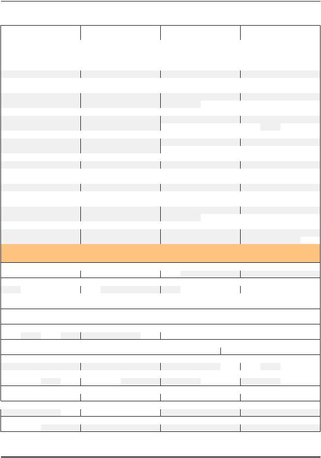
Register Quick Reference
31 |
30 |
29 |
28 |
27 |
26 |
25 |
24 |
23 |
22 |
21 |
20 |
19 |
18 |
17 |
16 |
15 |
14 |
13 |
12 |
11 |
10 |
9 |
8 |
7 |
6 |
5 |
4 |
3 |
2 |
1 |
0 |
MACIA0, type R/W, offset 0x014, reset 0x0000.0000 |
|
|
|
|
|
|
|
|
|
|
|
||||
|
|
|
MACOCT4 |
|
|
|
|
|
|
MACOCT3 |
|
|
|
||
|
|
|
MACOCT2 |
|
|
|
|
|
|
MACOCT1 |
|
|
|
||
MACIA1, type R/W, offset 0x018, reset 0x0000.0000 |
|
|
|
|
|
|
|
|
|
|
|
||||
|
|
|
MACOCT6 |
|
|
|
|
|
|
MACOCT5 |
|
|
|
||
MACTHR, type R/W, offset 0x01C, reset 0x0000.003F |
|
|
|
|
|
|
|
|
|
|
|
||||
|
|
|
|
|
|
|
|
|
|
|
|
THRESH |
|
|
|
MACMCTL, type R/W, offset 0x020, reset 0x0000.0000 |
|
|
|
|
|
|
|
|
|
|
|
||||
|
|
|
|
|
|
|
|
|
|
REGADR |
|
|
|
WRITE |
START |
MACMDV, type R/W, offset 0x024, reset 0x0000.0080 |
|
|
|
|
|
|
|
|
|
|
|
||||
|
|
|
|
|
|
|
|
|
|
|
DIV |
|
|
|
|
MACMTXD, type R/W, offset 0x02C, reset 0x0000.0000 |
|
|
|
|
|
|
|
|
|
|
|||||
|
|
|
|
|
|
|
MDTX |
|
|
|
|
|
|
|
|
MACMRXD, type R/W, offset 0x030, reset 0x0000.0000 |
|
|
|
|
|
|
|
|
|
|
|||||
|
|
|
|
|
|
|
MDRX |
|
|
|
|
|
|
|
|
MACNP, type RO, offset 0x034, reset 0x0000.0000 |
|
|
|
|
|
|
|
|
|
|
|
||||
|
|
|
|
|
|
|
|
|
|
|
|
NPR |
|
|
|
MACTR, type R/W, offset 0x038, reset 0x0000.0000 |
|
|
|
|
|
|
|
|
|
|
|
||||
|
|
|
|
|
|
|
|
|
|
|
|
|
|
|
NEWTX |
Ethernet Controller |
|
|
|
|
|
|
|
|
|
|
|
|
|
||
MII Management |
|
|
|
|
|
|
|
|
|
|
|
|
|
||
MR0, type R/W, address 0x00, reset 0x3100 |
|
|
|
|
|
|
|
|
|
|
|
||||
RESET |
LOOPBK |
SPEEDSL |
ANEGEN |
PWRDN |
ISO |
RANEG |
DUPLEX |
COLT |
|
|
|
|
|
|
|
MR1, type RO, address 0x01, reset 0x7849 |
|
|
|
|
|
|
|
|
|
|
|
|
|||
|
100X_F |
100X_H 10T_F |
10T_H |
|
|
|
|
MFPS |
ANEGC |
RFAULT |
ANEGA |
LINK |
JAB |
EXTD |
|
MR2, type RO, address 0x02, reset 0x000E |
|
|
|
|
|
|
|
|
|
|
|
|
|||
|
|
|
|
|
|
|
OUI[21:6] |
|
|
|
|
|
|
|
|
MR3, type RO, address 0x03, reset 0x7237 |
|
|
|
|
|
|
|
|
|
|
|
|
|||
|
|
OUI[5:0] |
|
|
|
|
MN |
|
|
|
RN |
|
|||
MR4, type R/W, address 0x04, reset 0x01E1 |
|
|
|
|
|
|
|
|
|
|
|
||||
NP |
|
RF |
|
|
|
|
A3 |
A2 |
A1 |
A0 |
|
|
S |
|
|
MR5, type RO, address 0x05, reset 0x0000 |
|
|
|
|
|
|
|
|
|
|
|
|
|||
NP |
ACK |
RF |
|
|
|
A[7:0] |
|
|
|
|
|
S |
|
|
|
MR6, type RO, address 0x06, reset 0x0000 |
|
|
|
|
|
|
|
|
|
|
|
|
|||
|
|
|
|
|
|
|
|
|
|
|
LPNPA |
|
PRX |
LPANEGA |
|
MR16, type R/W, address 0x10, reset 0x0140 |
|
|
|
|
|
|
|
|
|
|
|
||||
RPTR |
INPOL |
|
TXHIM |
SQEI |
NL10 |
|
|
|
|
APOL |
RVSPOL |
|
|
PCSBP |
RXCC |
MR17, type R/W, address 0x11, reset 0x0000 |
|
|
|
|
|
|
|
|
|
|
|
||||
JABBER_IE |
RXER_IE |
PRX_IE |
PDF_IE |
LPACK_IE |
LSCHG_IE |
RFAULT_IE |
ANEGCOMP_IE |
JABBER_INT |
RXER_INT |
PRX_INT |
PDF_INT |
LPACK_INT |
LSCHG_INT |
RFAULT_INT |
ANEGCOMP_INT |
 MR18, type RO, address 0x12, reset 0x0000
ANEGF DPLX RATE RXSD RX_LOCK
MR19, type R/W, address 0x13, reset 0x4000
TXO
608 |
November 16, 2008 |
Preliminary

LM3S6965 Microcontroller
31 |
30 |
29 |
28 |
27 |
26 |
25 |
24 |
23 |
22 |
21 |
20 |
19 |
18 |
17 |
16 |
15 |
14 |
13 |
12 |
11 |
10 |
9 |
8 |
7 |
6 |
5 |
4 |
3 |
2 |
1 |
0 |
MR23, type R/W, address 0x17, reset 0x0010 |
|
|
|
|
|
|
|
|
|
|
|
|
|||
|
|
|
|
|
|
|
|
|
LED1[3:0] |
|
|
LED0[3:0] |
|
||
MR24, type R/W, address 0x18, reset 0x00C0 |
|
|
|
|
|
|
|
|
|
|
|
|
|||
|
|
|
|
|
|
|
|
PD_MODE AUTO_SW |
MDIX |
MDIX_CM |
|
MDIX_SD |
|
||
Analog Comparators
Base 0x4003.C000
 ACMIS, type R/W1C, offset 0x000, reset 0x0000.0000
IN1  IN0
IN0
ACRIS, type RO, offset 0x004, reset 0x0000.0000
IN1  IN0
IN0
ACINTEN, type R/W, offset 0x008, reset 0x0000.0000
IN1 IN0
 ACREFCTL, type R/W, offset 0x010, reset 0x0000.0000
EN |
RNG |
VREF |
 ACSTAT0, type RO, offset 0x020, reset 0x0000.0000
OVAL
 ACSTAT1, type RO, offset 0x040, reset 0x0000.0000
|
|
|
|
|
|
OVAL |
ACCTL0, type R/W, offset 0x024, reset 0x0000.0000 |
|
|
|
|
|
|
TOEN |
ASRCP |
TSLVAL |
TSEN |
ISLVAL |
ISEN |
CINV |
ACCTL1, type R/W, offset 0x044, reset 0x0000.0000 |
|
|
|
|
|
|
TOEN |
ASRCP |
TSLVAL |
TSEN |
ISLVAL |
ISEN |
CINV |
Pulse Width Modulator (PWM)
Base 0x4002.8000
 PWMCTL, type R/W, offset 0x000, reset 0x0000.0000
GlobalSync2 GlobalSync1 GlobalSync0
 PWMSYNC, type R/W, offset 0x004, reset 0x0000.0000
Sync2  Sync1
Sync1  Sync0
Sync0
PWMENABLE, type R/W, offset 0x008, reset 0x0000.0000


 PWM5En
  PWM4En
  PWM3En
  PWM2En
  PWM1En
  PWM0En
PWMINVERT, type R/W, offset 0x00C, reset 0x0000.0000


 PWM5Inv
 PWM4Inv
 PWM3Inv
 PWM2Inv
 PWM1Inv
 PWM0Inv
PWMFAULT, type R/W, offset 0x010, reset 0x0000.0000
 PWMINTEN, type R/W, offset 0x014, reset 0x0000.0000
Fault5  Fault4
  Fault3
  Fault2
  Fault1
  Fault0


 IntFault
IntPWM2 IntPWM1 IntPWM0
November 16, 2008 |
609 |
Preliminary

Register Quick Reference
31 |
30 |
29 |
28 |
27 |
26 |
25 |
24 |
23 |
22 |
21 |
20 |
19 |
18 |
17 |
16 |
15 |
14 |
13 |
12 |
11 |
10 |
9 |
8 |
7 |
6 |
5 |
4 |
3 |
2 |
1 |
0 |
PWMRIS, type RO, offset 0x018, reset 0x0000.0000 |
|
|
|
|
|
|
|
|
|
|
|
||||
|
|
|
|
|
|
|
|
|
|
|
|
|
|
|
IntFault |
|
|
|
|
|
|
|
|
|
|
|
|
|
IntPWM2 |
IntPWM1 |
IntPWM0 |
PWMISC, type R/W1C, offset 0x01C, reset 0x0000.0000 |
|
|
|
|
|
|
|
|
|
|
|||||
|
|
|
|
|
|
|
|
|
|
|
|
|
|
|
IntFault |
|
|
|
|
|
|
|
|
|
|
|
|
|
IntPWM2 |
IntPWM1 |
IntPWM0 |
PWMSTATUS, type RO, offset 0x020, reset 0x0000.0000 |
|
|
|
|
|
|
|
|
|
|
|||||
|
|
|
|
|
|
|
|
|
|
|
|
|
|
|
Fault |
PWM0CTL, type R/W, offset 0x040, reset 0x0000.0000 |
|
|
|
|
|
|
|
|
|
|
|
||||
|
|
|
|
|
|
|
|
|
|
CmpBUpd |
CmpAUpd |
LoadUpd |
Debug |
Mode |
Enable |
PWM1CTL, type R/W, offset 0x080, reset 0x0000.0000 |
|
|
|
|
|
|
|
|
|
|
|
||||
|
|
|
|
|
|
|
|
|
|
CmpBUpd |
CmpAUpd |
LoadUpd |
Debug |
Mode |
Enable |
PWM2CTL, type R/W, offset 0x0C0, reset 0x0000.0000 |
|
|
|
|
|
|
|
|
|
|
|
||||
|
|
|
|
|
|
|
|
|
|
CmpBUpd |
CmpAUpd |
LoadUpd |
Debug |
Mode |
Enable |
PWM0INTEN, type R/W, offset 0x044, reset 0x0000.0000 |
|
|
|
|
|
|
|
|
|
|
|||||
|
|
TrCmpBD |
TrCmpBU |
TrCmpAD |
TrCmpAU |
TrCntLoad |
TrCntZero |
|
|
IntCmpBD |
IntCmpBU |
IntCmpAD |
IntCmpAU |
IntCntLoad |
IntCntZero |
PWM1INTEN, type R/W, offset 0x084, reset 0x0000.0000 |
|
|
|
|
|
|
|
|
|
|
|||||
|
|
TrCmpBD |
TrCmpBU |
TrCmpAD |
TrCmpAU |
TrCntLoad |
TrCntZero |
|
|
IntCmpBD |
IntCmpBU |
IntCmpAD |
IntCmpAU |
IntCntLoad |
IntCntZero |
PWM2INTEN, type R/W, offset 0x0C4, reset 0x0000.0000 |
|
|
|
|
|
|
|
|
|
|
|||||
|
|
TrCmpBD |
TrCmpBU |
TrCmpAD |
TrCmpAU |
TrCntLoad |
TrCntZero |
|
|
IntCmpBD |
IntCmpBU |
IntCmpAD |
IntCmpAU |
IntCntLoad |
IntCntZero |
PWM0RIS, type RO, offset 0x048, reset 0x0000.0000 |
|
|
|
|
|
|
|
|
|
|
|
||||
|
|
|
|
|
|
|
|
|
|
IntCmpBD IntCmpBU IntCmpAD IntCmpAU IntCntLoad |
IntCntZero |
||||
PWM1RIS, type RO, offset 0x088, reset 0x0000.0000 |
|
|
|
|
|
|
|
|
|
|
|
||||
|
|
|
|
|
|
|
|
|
|
IntCmpBD IntCmpBU IntCmpAD IntCmpAU IntCntLoad |
IntCntZero |
||||
PWM2RIS, type RO, offset 0x0C8, reset 0x0000.0000 |
|
|
|
|
|
|
|
|
|
|
|
||||
|
|
|
|
|
|
|
|
|
|
IntCmpBD IntCmpBU IntCmpAD IntCmpAU IntCntLoad |
IntCntZero |
||||
PWM0ISC, type R/W1C, offset 0x04C, reset 0x0000.0000 |
|
|
|
|
|
|
|
|
|
|
|||||
|
|
|
|
|
|
|
|
|
|
IntCmpBD IntCmpBU IntCmpAD IntCmpAU IntCntLoad |
IntCntZero |
||||
PWM1ISC, type R/W1C, offset 0x08C, reset 0x0000.0000 |
|
|
|
|
|
|
|
|
|
|
|||||
|
|
|
|
|
|
|
|
|
|
IntCmpBD IntCmpBU IntCmpAD IntCmpAU IntCntLoad |
IntCntZero |
||||
PWM2ISC, type R/W1C, offset 0x0CC, reset 0x0000.0000 |
|
|
|
|
|
|
|
|
|
|
|||||
|
|
|
|
|
|
|
|
|
|
IntCmpBD IntCmpBU IntCmpAD IntCmpAU IntCntLoad |
IntCntZero |
||||
PWM0LOAD, type R/W, offset 0x050, reset 0x0000.0000 |
|
|
|
|
|
|
|
|
|
|
|||||
Load
 PWM1LOAD, type R/W, offset 0x090, reset 0x0000.0000
Load
610 |
November 16, 2008 |
Preliminary
LM3S6965 Microcontroller
31 |
30 |
29 |
28 |
27 |
26 |
25 |
24 |
23 |
22 |
21 |
20 |
19 |
18 |
17 |
16 |
15 |
14 |
13 |
12 |
11 |
10 |
9 |
8 |
7 |
6 |
5 |
4 |
3 |
2 |
1 |
0 |
 PWM2LOAD, type R/W, offset 0x0D0, reset 0x0000.0000
Load
 PWM0COUNT, type RO, offset 0x054, reset 0x0000.0000
Count
 PWM1COUNT, type RO, offset 0x094, reset 0x0000.0000
Count
 PWM2COUNT, type RO, offset 0x0D4, reset 0x0000.0000
Count
 PWM0CMPA, type R/W, offset 0x058, reset 0x0000.0000
CompA
 PWM1CMPA, type R/W, offset 0x098, reset 0x0000.0000
CompA
 PWM2CMPA, type R/W, offset 0x0D8, reset 0x0000.0000
CompA
 PWM0CMPB, type R/W, offset 0x05C, reset 0x0000.0000
CompB
 PWM1CMPB, type R/W, offset 0x09C, reset 0x0000.0000
CompB
 PWM2CMPB, type R/W, offset 0x0DC, reset 0x0000.0000
CompB
 PWM0GENA, type R/W, offset 0x060, reset 0x0000.0000
ActCmpBD |
ActCmpBU |
ActCmpAD |
ActCmpAU |
ActLoad |
ActZero |
 PWM1GENA, type R/W, offset 0x0A0, reset 0x0000.0000
ActCmpBD |
ActCmpBU |
ActCmpAD |
ActCmpAU |
ActLoad |
ActZero |
 PWM2GENA, type R/W, offset 0x0E0, reset 0x0000.0000
ActCmpBD |
ActCmpBU |
ActCmpAD |
ActCmpAU |
ActLoad |
ActZero |
 PWM0GENB, type R/W, offset 0x064, reset 0x0000.0000
ActCmpBD |
ActCmpBU |
ActCmpAD |
ActCmpAU |
ActLoad |
ActZero |
 PWM1GENB, type R/W, offset 0x0A4, reset 0x0000.0000
ActCmpBD |
ActCmpBU |
ActCmpAD |
ActCmpAU |
ActLoad |
ActZero |
 PWM2GENB, type R/W, offset 0x0E4, reset 0x0000.0000
ActCmpBD |
ActCmpBU |
ActCmpAD |
ActCmpAU |
ActLoad |
ActZero |
 PWM0DBCTL, type R/W, offset 0x068, reset 0x0000.0000


 Enable
November 16, 2008 |
611 |
Preliminary
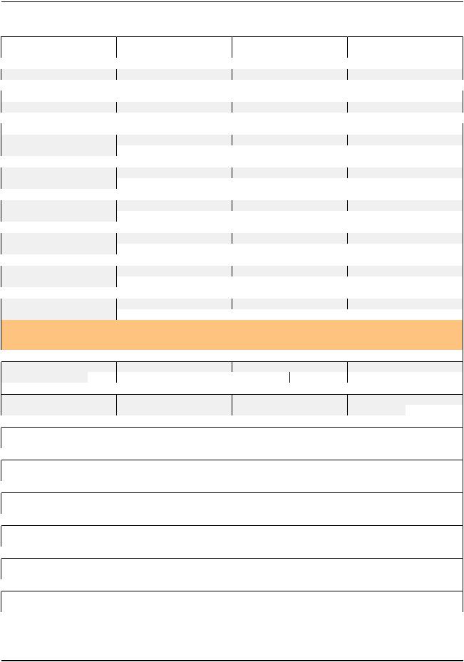
Register Quick Reference
31 |
30 |
29 |
28 |
27 |
26 |
25 |
24 |
23 |
22 |
21 |
20 |
19 |
18 |
17 |
16 |
15 |
14 |
13 |
12 |
11 |
10 |
9 |
8 |
7 |
6 |
5 |
4 |
3 |
2 |
1 |
0 |
 PWM1DBCTL, type R/W, offset 0x0A8, reset 0x0000.0000


 Enable
PWM2DBCTL, type R/W, offset 0x0E8, reset 0x0000.0000


 Enable
PWM0DBRISE, type R/W, offset 0x06C, reset 0x0000.0000
RiseDelay
 PWM1DBRISE, type R/W, offset 0x0AC, reset 0x0000.0000
RiseDelay
 PWM2DBRISE, type R/W, offset 0x0EC, reset 0x0000.0000
RiseDelay
 PWM0DBFALL, type R/W, offset 0x070, reset 0x0000.0000
FallDelay
 PWM1DBFALL, type R/W, offset 0x0B0, reset 0x0000.0000
FallDelay
 PWM2DBFALL, type R/W, offset 0x0F0, reset 0x0000.0000
FallDelay
Quadrature Encoder Interface (QEI)
QEI0 base: 0x4002.C000
QEI1 base: 0x4002.D000
 QEICTL, type R/W, offset 0x000, reset 0x0000.0000
STALLEN |
INVI |
INVB |
INVA |
VelDiv |
VelEn ResMode CapMode SigMode Swap |
Enable |
QEISTAT, type RO, offset 0x004, reset 0x0000.0000 |
|
|
|
|
|
|
|
|
|
|
|
Direction |
Error |
 QEIPOS, type R/W, offset 0x008, reset 0x0000.0000
Position
Position
 QEIMAXPOS, type R/W, offset 0x00C, reset 0x0000.0000
MaxPos
MaxPos
 QEILOAD, type R/W, offset 0x010, reset 0x0000.0000
Load
Load
 QEITIME, type RO, offset 0x014, reset 0x0000.0000
Time
Time
 QEICOUNT, type RO, offset 0x018, reset 0x0000.0000
Count
Count
 QEISPEED, type RO, offset 0x01C, reset 0x0000.0000
Speed
Speed
612 |
November 16, 2008 |
Preliminary

LM3S6965 Microcontroller
31 |
30 |
29 |
28 |
27 |
26 |
25 |
24 |
23 |
22 |
21 |
20 |
19 |
18 |
17 |
16 |
15 |
14 |
13 |
12 |
11 |
10 |
9 |
8 |
7 |
6 |
5 |
4 |
3 |
2 |
1 |
0 |
QEIINTEN, type R/W, offset 0x020, reset 0x0000.0000 |
|
|
|
|
|
|
|
|
|
|
|
||||
|
|
|
|
|
|
|
|
|
|
|
|
IntError |
IntDir |
IntTimer |
IntIndex |
QEIRIS, type RO, offset 0x024, reset 0x0000.0000 |
|
|
|
|
|
|
|
|
|
|
|
||||
|
|
|
|
|
|
|
|
|
|
|
|
IntError |
IntDir |
IntTimer |
IntIndex |
QEIISC, type R/W1C, offset 0x028, reset 0x0000.0000 |
|
|
|
|
|
|
|
|
|
|
|
||||
|
|
|
|
|
|
|
|
|
|
|
|
IntError |
IntDir |
IntTimer |
IntIndex |
November 16, 2008 |
613 |
Preliminary
Ordering and Contact Information
COrdering and Contact Information
C.1 Ordering Information
L M 3 S n n n n – g p p s s – r r m
Part Number  nnn = Sandstorm-class parts nnnn = All other Stellaris® parts
Temperature
E = –40 C to +105 C I = –40 C to +85 C
Package
BZ = 108-ball BGA
QC = 100-pin LQFP
QN = 48-pin LQFP
QR = 64-pin LQFP
RN = 28-pin SOIC
Speed
20 = 20 MHz
25 = 25 MHz
50 = 50 MHz
80 = 80 MHz
Table C-1. Part Ordering Information
Orderable Part Number |
Description |
LM3S6965-IBZ50 |
Stellaris® LM3S6965 Microcontroller |
LM3S6965-IBZ50 (T) |
Stellaris® LM3S6965 Microcontroller |
LM3S6965-EQC50 |
Stellaris® LM3S6965 Microcontroller |
LM3S6965-EQC50 (T) |
Stellaris® LM3S6965 Microcontroller |
LM3S6965-IQC50 |
Stellaris® LM3S6965 Microcontroller |
LM3S6965-IQC50 (T) |
Stellaris® LM3S6965 Microcontroller |
Shipping Medium
T = Tape-and-reel
Omitted = Default shipping (tray or tube)
Revision
Omitted = Default to current shipping revision A0 = First all-layer mask
A1 = Metal layers update to A0
A2 = Metal layers update to A1
B0 = Second all-layer mask revision
C.2 Kits
TheLuminaryMicroStellaris® Familyprovidesthehardwareandsoftwaretoolsthatengineersneed to begin development quickly.
■ReferenceDesignKitsaccelerateproductdevelopmentbyprovidingready-to-runhardware,and comprehensive documentation including hardware design files:
http://www.luminarymicro.com/products/reference_design_kits/
■Evaluation Kits provide a low-cost and effective means of evaluating Stellaris® microcontrollers before purchase:
http://www.luminarymicro.com/products/kits.html
■Development Kits provide you with all the tools you need to develop and prototype embedded applications right out of the box:
http://www.luminarymicro.com/products/development_kits.html
SeetheLuminaryMicrowebsiteforthelatesttoolsavailable,oraskyourLuminaryMicrodistributor.
614 |
November 16, 2008 |
Preliminary

LM3S6965 Microcontroller
C.3 Company Information
Luminary Micro, Inc. designs, markets, and sells ARM Cortex-M3-based microcontrollers (MCUs). Austin, Texas-based Luminary Micro is the lead partner for the Cortex-M3 processor, delivering the world's first silicon implementation of the Cortex-M3 processor. Luminary Micro's introduction of the Stellaris®familyofproductsprovides32-bitperformanceforthesamepriceascurrent8- and16-bit microcontroller designs. With entry-level pricing at $1.00 for an ARM technology-based MCU, Luminary Micro's Stellaris product line allows for standardization that eliminates future architectural upgrades or software tool changes.
Luminary Micro, Inc. 108 Wild Basin, Suite 350 Austin, TX 78746
Main: +1-512-279-8800
Fax: +1-512-279-8879 http://www.luminarymicro.com sales@luminarymicro.com
C.4 Support Information
For support on Luminary Micro products, contact:
support@luminarymicro.com +1-512-279-8800, ext. 3
November 16, 2008 |
615 |
Preliminary