

Добавил:
Upload
Опубликованный материал нарушает ваши авторские права? Сообщите нам.
Вуз:
Предмет:
Файл:даташитина PIC 12F683 .pdf
X
- •8-Pin Flash-Based, 8-Bit CMOS Microcontrollers with nanoWatt Technology
- •1.0 Device Overview
- •2.0 Memory Organization
- •2.1 Program Memory Organization
- •FIGURE 2-1: Program Memory Map and Stack for the PIC12F683
- •2.2 Data Memory Organization
- •2.2.1 General Purpose Register File
- •2.2.2 Special Function Registers
- •FIGURE 2-2: Data Memory Map of the PIC12F683
- •2.3 PCL and PCLATH
- •FIGURE 2-3: Loading of PC in Different Situations
- •2.3.2 Stack
- •2.4 Indirect Addressing, INDF and FSR Registers
- •EXAMPLE 2-1: Indirect Addressing
- •3.1 Overview
- •FIGURE 3-1: PIC® MCU Clock Source Block Diagram
- •3.2 Oscillator Control
- •3.3 Clock Source Modes
- •3.4 External Clock Modes
- •TABLE 3-1: Oscillator Delay Examples
- •3.4.2 EC Mode
- •FIGURE 3-2: External Clock (EC) Mode Operation
- •3.4.3 LP, XT, HS Modes
- •FIGURE 3-3: Quartz Crystal Operation (LP, XT or HS Mode)
- •3.4.4 External RC Modes
- •FIGURE 3-5: External RC Modes
- •3.5 Internal Clock Modes
- •3.5.1 INTOSC and INTOSCIO Modes
- •3.5.2 HFINTOSC
- •3.5.3 LFINTOSC
- •3.5.4 Frequency Select Bits (IRCF)
- •3.5.5 HF and LF INTOSC Clock Switch Timing
- •FIGURE 3-6: Internal Oscillator Switch Timing
- •3.6 Clock Switching
- •3.6.1 System Clock Select (SCS) Bit
- •FIGURE 3-7: Two-Speed Start-up
- •FIGURE 3-8: FSCM Block Diagram
- •4.0 GPIO Port
- •4.1 GPIO and the TRISIO Registers
- •4.2 Additional Pin Functions
- •4.2.1 ANSEL Register
- •4.2.3 Interrupt-on-Change
- •Register 4-3: ANSEL: Analog Select Register
- •4.2.5 Pin Descriptions and Diagrams
- •FIGURE 4-1: Block Diagram of GP0
- •FIGURE 4-2: Block Diagram of GP1
- •FIGURE 4-4: Block Diagram of GP3
- •FIGURE 4-5: Block Diagram of GP4
- •FIGURE 4-6: Block Diagram of GP5
- •5.0 Timer0 Module
- •5.1 Timer0 Operation
- •FIGURE 5-1: Block Diagram of the Timer0/WDT Prescaler
- •5.1.3 Software Programmable Prescaler
- •5.1.4 Timer0 Interrupt
- •5.1.5 Using Timer0 with an External Clock
- •6.0 Timer1 Module with Gate Control
- •6.1 Timer1 Operation
- •6.2 Clock Source Selection
- •FIGURE 6-1: Timer1 Block Diagram
- •6.2.1 iNternal Clock Source
- •6.2.2 External Clock Source
- •6.3 Timer1 Prescaler
- •6.4 Timer1 Oscillator
- •6.5 Timer1 Operation in Asynchronous Counter Mode
- •6.5.1 Reading and Writing Timer1 in Asynchronous Counter Mode
- •6.6 Timer1 Gate
- •6.7 Timer1 Interrupt
- •6.8 Timer1 Operation During Sleep
- •6.9 CCP Special Event Trigger
- •6.10 Comparator Synchronization
- •FIGURE 6-2: Timer1 Incrementing Edge
- •6.11 Timer1 Control Register
- •7.0 Timer2 Module
- •7.1 Timer2 Operation
- •FIGURE 7-1: Timer2 Block Diagram
- •8.0 Comparator Module
- •8.1 Comparator Overview
- •FIGURE 8-1: Single Comparator
- •FIGURE 8-2: Comparator Output Block Diagram
- •8.2 Analog Input Connection Considerations
- •8.3 Comparator Configuration
- •8.4 Comparator Control
- •8.4.1 Comparator Output State
- •8.4.2 Comparator Output Polarity
- •8.4.3 Comparator Input Switch
- •8.5 Comparator Response Time
- •8.6 Comparator Interrupt Operation
- •8.7 Operation During Sleep
- •8.8 Effects of a Reset
- •8.9 Comparator Gating Timer1
- •8.10 Synchronizing Comparator Output to Timer1
- •8.11 Comparator Voltage Reference
- •8.11.1 Independent Operation
- •8.11.2 Output Voltage Selection
- •EQUATION 8-1: CVref Output Voltage
- •8.11.4 Output Ratiometric to Vdd
- •FIGURE 8-7: Comparator Voltage Reference Block Diagram
- •TABLE 8-2: Summary of Registers Associated with the Comparator and Voltage Reference Modules
- •FIGURE 9-1: ADC Block Diagram
- •9.1 ADC Configuration
- •9.1.1 GPIO Configuration
- •9.1.2 Channel Selection
- •9.1.4 Conversion Clock
- •FIGURE 9-2: Analog-to-Digital Conversion Tad Cycles
- •9.1.5 Interrupts
- •9.1.6 Result Formatting
- •9.2 ADC Operation
- •9.2.1 Starting a Conversion
- •9.2.2 Completion of a Conversion
- •9.2.3 Terminating a conversion
- •9.2.4 ADC Operation During Sleep
- •9.2.5 Special Event Trigger
- •9.2.6 A/D Conversion Procedure
- •EXAMPLE 9-1: A/D Conversion
- •9.2.7 ADC Register Definitions
- •9.3 A/D Acquisition Requirements
- •EQUATION 9-1: Acquisition Time Example
- •FIGURE 9-5: ADC Transfer Function
- •10.0 Data EEPROM Memory
- •10.1 EECON1 and EECON2 Registers
- •EXAMPLE 10-1: DATA EEPROM READ
- •EXAMPLE 10-2: DATA EEPROM WRITE
- •10.4 Write Verify
- •EXAMPLE 10-3: WRITE VERIFY
- •10.4.1 Using the Data EEPROM
- •10.5 Protection Against Spurious Write
- •TABLE 10-1: Summary of Associated Data EEPROM Registers
- •11.0 Capture/Compare/PWM (CCP) Module
- •TABLE 11-1: CCP Mode – Timer Resources Required
- •11.1 Capture Mode
- •11.1.1 CCP1 pin Configuration
- •11.1.2 Timer1 Mode Selection
- •11.1.3 Software Interrupt
- •11.1.4 CCP Prescaler
- •11.2 Compare Mode
- •11.2.1 CCP1 Pin Configuration
- •11.2.2 timer1 Mode Selection
- •11.2.3 Software Interrupt Mode
- •11.2.4 Special Event Trigger
- •11.3 PWM Mode
- •FIGURE 11-3: Simplified PWM Block Diagram
- •FIGURE 11-4: CCP PWM Output
- •11.3.1 PWM period
- •EQUATION 11-1: PWM Period
- •11.3.2 PWM Duty Cycle
- •EQUATION 11-2: Pulse Width
- •EQUATION 11-3: Duty Cycle Ratio
- •11.3.3 PWM Resolution
- •EQUATION 11-4: PWM Resolution
- •11.3.4 Operation in Sleep Mode
- •11.3.5 Changes in System Clock Frequency
- •11.3.6 Effects of Reset
- •11.3.7 Setup for PWM Operation
- •TABLE 11-4: Registers Associated with Capture, cOMPARE and Timer1
- •12.0 Special Features of the CPU
- •12.1 Configuration Bits
- •12.2 Calibration Bits
- •12.3 Reset
- •FIGURE 12-1: Simplified Block Diagram of On-Chip Reset Circuit
- •12.3.2 MCLR
- •FIGURE 12-2: Recommended MCLR Circuit
- •12.3.5 BOR Calibration
- •12.3.7 Power Control (PCON) Register
- •TABLE 12-1: Time-out in Various Situations
- •TABLE 12-2: Status/PCON Bits and Their Significance
- •TABLE 12-3: Summary of Registers Associated with Brown-out Reset
- •FIGURE 12-4: Time-out Sequence on Power-up (Delayed MCLR)
- •FIGURE 12-5: Time-out Sequence on Power-up (Delayed MCLR)
- •FIGURE 12-6: Time-out Sequence on Power-up (MCLR with Vdd)
- •TABLE 12-5: Initialization Condition for Special Registers
- •12.4 Interrupts
- •12.4.1 GP2/INT Interrupt
- •12.4.2 Timer0 Interrupt
- •12.4.3 GPIO Interrupt
- •FIGURE 12-7: Interrupt Logic
- •TABLE 12-6: Summary of Registers Associated with Interrupts
- •12.5 Context Saving During Interrupts
- •12.6 Watchdog Timer (WDT)
- •12.6.1 WDT Oscillator
- •12.6.2 WDT Control
- •TABLE 12-7: WDT Status
- •TABLE 12-8: Summary of Registers Associated with Watchdog Timer
- •12.8 Code Protection
- •12.9 ID Locations
- •12.10 In-Circuit Serial Programming™
- •FIGURE 12-11: Typical In-Circuit Serial Programming Connection
- •12.11 In-Circuit Debugger
- •TABLE 12-9: Debugger Resources
- •FIGURE 12-12: 14-Pin ICD Pinout
- •13.0 Instruction Set Summary
- •13.2 Instruction Descriptions
- •14.0 Development Support
- •14.1 MPLAB Integrated Development Environment Software
- •14.2 MPASM Assembler
- •14.3 MPLAB C18 and MPLAB C30 C Compilers
- •14.4 MPLINK Object Linker/ MPLIB Object Librarian
- •14.5 MPLAB ASM30 Assembler, Linker and Librarian
- •14.6 MPLAB SIM Software Simulator
- •14.10 MPLAB PM3 Device Programmer
- •14.11 PICSTART Plus Development Programmer
- •14.12 PICkit 2 Development Programmer
- •14.13 Demonstration, Development and Evaluation Boards
- •15.0 Electrical Specifications
- •FIGURE 15-2: HFINTOSC Frequency Accuracy Over Device Vdd and Temperature
- •15.6 Thermal Considerations
- •15.7 Timing Parameter Symbology
- •FIGURE 15-3: Load Conditions
- •15.8 AC Characteristics: PIC12F683 (Industrial, Extended)
- •TABLE 15-1: Clock Oscillator Timing Requirements
- •TABLE 15-2: Oscillator Parameters
- •FIGURE 15-5: CLKOUT and I/O Timing
- •TABLE 15-3: CLKOUT and I/O Timing Parameters
- •FIGURE 15-6: Reset, Watchdog Timer, Oscillator Start-up Timer and Power-up Timer Timing
- •FIGURE 15-7: Brown-out Reset Timing and Characteristics
- •FIGURE 15-8: Timer0 and Timer1 External Clock Timings
- •TABLE 15-5: Timer0 and Timer1 External Clock Requirements
- •FIGURE 15-9: Capture/Compare/PWM Timings (ECCP)
- •TABLE 15-6: Capture/Compare/PWM Requirements (ECCP)
- •TABLE 15-7: Comparator Specifications
- •TABLE 15-8: Comparator Voltage Reference (CVref) Specifications
- •TABLE 15-9: PIC12F683 A/D Converter (ADC) Characteristics
- •TABLE 15-10: PIC12F683 A/D Conversion Requirements
- •FIGURE 15-10: PIC12F683 A/D Conversion Timing (Normal Mode)
- •FIGURE 15-11: PIC12F683 A/D Conversion Timing (Sleep Mode)
- •16.0 DC and AC Characteristics Graphs and Tables
- •FIGURE 16-1: Typical Idd vs. Fosc Over Vdd (EC Mode)
- •FIGURE 16-2: Maximum Idd vs. Fosc Over Vdd (EC Mode)
- •FIGURE 16-3: Typical Idd vs. Fosc Over Vdd (HS Mode)
- •FIGURE 16-4: Maximum Idd vs. Fosc Over Vdd (HS Mode)
- •FIGURE 16-5: Typical Idd vs. Vdd Over Fosc (XT Mode)
- •FIGURE 16-6: Maximum Idd vs. Vdd Over Fosc (XT Mode)
- •FIGURE 16-7: Typical Idd vs. Vdd Over Fosc (EXTRC Mode)
- •FIGURE 16-8: Maximum Idd vs. Vdd (EXTRC Mode)
- •FIGURE 16-9: Idd vs. Vdd Over Fosc (LFINTOSC Mode, 31 kHz)
- •FIGURE 16-10: Idd vs. Vdd (LP Mode)
- •FIGURE 16-11: Typical Idd vs. Fosc Over Vdd (HFINTOSC Mode)
- •FIGURE 16-12: Maximum Idd vs. Fosc Over Vdd (HFINTOSC Mode)
- •FIGURE 16-13: Typical Ipd vs. Vdd (Sleep Mode, all Peripherals Disabled)
- •FIGURE 16-14: Maximum Ipd vs. Vdd (Sleep Mode, all Peripherals Disabled)
- •FIGURE 16-15: Comparator Ipd vs. Vdd (Both Comparators Enabled)
- •FIGURE 16-16: BOR Ipd VS. Vdd Over Temperature
- •FIGURE 16-17: Typical WDT Ipd VS. Vdd Over Temperature
- •FIGURE 16-18: Maximum WDT Ipd VS. Vdd Over Temperature
- •FIGURE 16-19: WDT Period VS. Vdd Over Temperature
- •FIGURE 16-20: WDT Period VS. Temperature Over Vdd (5.0V)
- •FIGURE 16-21: CVref Ipd VS. Vdd Over Temperature (High Range)
- •FIGURE 16-22: CVref Ipd VS. Vdd Over Temperature (Low Range)
- •FIGURE 16-23: Vol VS. Iol Over Temperature (Vdd = 3.0V)
- •FIGURE 16-24: Vol VS. Iol Over Temperature (Vdd = 5.0V)
- •FIGURE 16-25: Voh VS. Ioh Over Temperature (Vdd = 3.0V)
- •FIGURE 16-26: Voh VS. Ioh Over Temperature (Vdd = 5.0V)
- •FIGURE 16-27: TTL Input Threshold Vin VS. Vdd Over Temperature
- •FIGURE 16-28: Schmitt Trigger Input Threshold Vin VS. Vdd Over Temperature
- •FIGURE 16-29: T1OSC Ipd vs. Vdd Over Temperature (32 kHz)
- •FIGURE 16-30: Comparator Response Time (Rising Edge)
- •FIGURE 16-31: Comparator Response Time (Falling Edge)
- •FIGURE 16-32: LFINTOSC Frequency vs. Vdd Over Temperature (31 kHz)
- •FIGURE 16-33: ADC Clock Period vs. Vdd Over Temperature
- •FIGURE 16-34: Typical HFINTOSC Start-Up Times vs. Vdd Over Temperature
- •FIGURE 16-36: Minimum HFINTOSC Start-Up Times vs. Vdd Over Temperature
- •17.0 Packaging Information
- •17.1 Package Marking Information
- •17.2 Package Details
- •Appendix A: Data Sheet Revision History
- •Appendix B: Migrating From Other PIC® Devices
- •INDEX
- •The Microchip Web Site
- •Customer Change Notification Service
- •Customer Support
- •Reader Response
- •Product Identification System
- •Worldwide Sales and Service
PIC12F683
15.7Timing Parameter Symbology
The timing parameter symbols have been created with one of the following formats:
1.TppS2ppS
2.TppS
T |
|
|
|
|
|
|
|
|
|
|
|
F |
Frequency |
T |
Time |
||||||||
Lowercase letters (pp) and their meanings: |
|
|
|
|
|
|
|
|
|||
pp |
|
|
|
|
|
|
|
|
|
|
|
cc |
CCP1 |
osc |
OSC1 |
||||||||
ck |
CLKOUT |
rd |
|
|
|
|
|
|
|||
RD |
|
|
|
|
|||||||
cs |
|
|
rw |
|
|
|
or |
|
|
||
CS |
|
|
RD |
|
WR |
|
|||||
di |
SDI |
sc |
SCK |
||||||||
do |
SDO |
ss |
|
|
|||||||
SS |
|
|
|||||||||
dt |
Data in |
t0 |
T0CKI |
||||||||
io |
I/O PORT |
t1 |
T1CKI |
||||||||
mc |
|
wr |
|
|
|||||||
MCLR |
|
WR |
|
||||||||
Uppercase letters and their meanings: |
|
|
|
|
|
|
|
|
|||
S |
|
|
|
|
|
|
|
|
|
|
|
F |
Fall |
P |
Period |
||||||||
H |
High |
R |
Rise |
||||||||
I |
Invalid (High-impedance) |
V |
Valid |
||||||||
L |
Low |
Z |
High-impedance |
||||||||
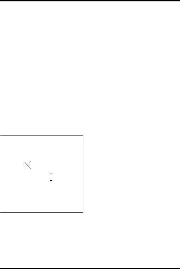
FIGURE 15-3: LOAD CONDITIONS
Load Condition
|
|
|
|
|
|
|
|
|
|
|
|
|
Pin |
|
|
CL |
|
|
|
||||
|
|
|
|
|
|
|
|
|
|
|
|
|
|
|
VSS |
||
Legend: CL = 50 pF |
for all pins |
||||
|
|
15 pF |
for OSC2 output |
||
DS41211D-page 124 |
♥ 2007 Microchip Technology Inc. |
Соседние файлы в предмете [НЕСОРТИРОВАННОЕ]