
- •8-Pin Flash-Based, 8-Bit CMOS Microcontrollers with nanoWatt Technology
- •1.0 Device Overview
- •2.0 Memory Organization
- •2.1 Program Memory Organization
- •FIGURE 2-1: Program Memory Map and Stack for the PIC12F683
- •2.2 Data Memory Organization
- •2.2.1 General Purpose Register File
- •2.2.2 Special Function Registers
- •FIGURE 2-2: Data Memory Map of the PIC12F683
- •2.3 PCL and PCLATH
- •FIGURE 2-3: Loading of PC in Different Situations
- •2.3.2 Stack
- •2.4 Indirect Addressing, INDF and FSR Registers
- •EXAMPLE 2-1: Indirect Addressing
- •3.1 Overview
- •FIGURE 3-1: PIC® MCU Clock Source Block Diagram
- •3.2 Oscillator Control
- •3.3 Clock Source Modes
- •3.4 External Clock Modes
- •TABLE 3-1: Oscillator Delay Examples
- •3.4.2 EC Mode
- •FIGURE 3-2: External Clock (EC) Mode Operation
- •3.4.3 LP, XT, HS Modes
- •FIGURE 3-3: Quartz Crystal Operation (LP, XT or HS Mode)
- •3.4.4 External RC Modes
- •FIGURE 3-5: External RC Modes
- •3.5 Internal Clock Modes
- •3.5.1 INTOSC and INTOSCIO Modes
- •3.5.2 HFINTOSC
- •3.5.3 LFINTOSC
- •3.5.4 Frequency Select Bits (IRCF)
- •3.5.5 HF and LF INTOSC Clock Switch Timing
- •FIGURE 3-6: Internal Oscillator Switch Timing
- •3.6 Clock Switching
- •3.6.1 System Clock Select (SCS) Bit
- •FIGURE 3-7: Two-Speed Start-up
- •FIGURE 3-8: FSCM Block Diagram
- •4.0 GPIO Port
- •4.1 GPIO and the TRISIO Registers
- •4.2 Additional Pin Functions
- •4.2.1 ANSEL Register
- •4.2.3 Interrupt-on-Change
- •Register 4-3: ANSEL: Analog Select Register
- •4.2.5 Pin Descriptions and Diagrams
- •FIGURE 4-1: Block Diagram of GP0
- •FIGURE 4-2: Block Diagram of GP1
- •FIGURE 4-4: Block Diagram of GP3
- •FIGURE 4-5: Block Diagram of GP4
- •FIGURE 4-6: Block Diagram of GP5
- •5.0 Timer0 Module
- •5.1 Timer0 Operation
- •FIGURE 5-1: Block Diagram of the Timer0/WDT Prescaler
- •5.1.3 Software Programmable Prescaler
- •5.1.4 Timer0 Interrupt
- •5.1.5 Using Timer0 with an External Clock
- •6.0 Timer1 Module with Gate Control
- •6.1 Timer1 Operation
- •6.2 Clock Source Selection
- •FIGURE 6-1: Timer1 Block Diagram
- •6.2.1 iNternal Clock Source
- •6.2.2 External Clock Source
- •6.3 Timer1 Prescaler
- •6.4 Timer1 Oscillator
- •6.5 Timer1 Operation in Asynchronous Counter Mode
- •6.5.1 Reading and Writing Timer1 in Asynchronous Counter Mode
- •6.6 Timer1 Gate
- •6.7 Timer1 Interrupt
- •6.8 Timer1 Operation During Sleep
- •6.9 CCP Special Event Trigger
- •6.10 Comparator Synchronization
- •FIGURE 6-2: Timer1 Incrementing Edge
- •6.11 Timer1 Control Register
- •7.0 Timer2 Module
- •7.1 Timer2 Operation
- •FIGURE 7-1: Timer2 Block Diagram
- •8.0 Comparator Module
- •8.1 Comparator Overview
- •FIGURE 8-1: Single Comparator
- •FIGURE 8-2: Comparator Output Block Diagram
- •8.2 Analog Input Connection Considerations
- •8.3 Comparator Configuration
- •8.4 Comparator Control
- •8.4.1 Comparator Output State
- •8.4.2 Comparator Output Polarity
- •8.4.3 Comparator Input Switch
- •8.5 Comparator Response Time
- •8.6 Comparator Interrupt Operation
- •8.7 Operation During Sleep
- •8.8 Effects of a Reset
- •8.9 Comparator Gating Timer1
- •8.10 Synchronizing Comparator Output to Timer1
- •8.11 Comparator Voltage Reference
- •8.11.1 Independent Operation
- •8.11.2 Output Voltage Selection
- •EQUATION 8-1: CVref Output Voltage
- •8.11.4 Output Ratiometric to Vdd
- •FIGURE 8-7: Comparator Voltage Reference Block Diagram
- •TABLE 8-2: Summary of Registers Associated with the Comparator and Voltage Reference Modules
- •FIGURE 9-1: ADC Block Diagram
- •9.1 ADC Configuration
- •9.1.1 GPIO Configuration
- •9.1.2 Channel Selection
- •9.1.4 Conversion Clock
- •FIGURE 9-2: Analog-to-Digital Conversion Tad Cycles
- •9.1.5 Interrupts
- •9.1.6 Result Formatting
- •9.2 ADC Operation
- •9.2.1 Starting a Conversion
- •9.2.2 Completion of a Conversion
- •9.2.3 Terminating a conversion
- •9.2.4 ADC Operation During Sleep
- •9.2.5 Special Event Trigger
- •9.2.6 A/D Conversion Procedure
- •EXAMPLE 9-1: A/D Conversion
- •9.2.7 ADC Register Definitions
- •9.3 A/D Acquisition Requirements
- •EQUATION 9-1: Acquisition Time Example
- •FIGURE 9-5: ADC Transfer Function
- •10.0 Data EEPROM Memory
- •10.1 EECON1 and EECON2 Registers
- •EXAMPLE 10-1: DATA EEPROM READ
- •EXAMPLE 10-2: DATA EEPROM WRITE
- •10.4 Write Verify
- •EXAMPLE 10-3: WRITE VERIFY
- •10.4.1 Using the Data EEPROM
- •10.5 Protection Against Spurious Write
- •TABLE 10-1: Summary of Associated Data EEPROM Registers
- •11.0 Capture/Compare/PWM (CCP) Module
- •TABLE 11-1: CCP Mode – Timer Resources Required
- •11.1 Capture Mode
- •11.1.1 CCP1 pin Configuration
- •11.1.2 Timer1 Mode Selection
- •11.1.3 Software Interrupt
- •11.1.4 CCP Prescaler
- •11.2 Compare Mode
- •11.2.1 CCP1 Pin Configuration
- •11.2.2 timer1 Mode Selection
- •11.2.3 Software Interrupt Mode
- •11.2.4 Special Event Trigger
- •11.3 PWM Mode
- •FIGURE 11-3: Simplified PWM Block Diagram
- •FIGURE 11-4: CCP PWM Output
- •11.3.1 PWM period
- •EQUATION 11-1: PWM Period
- •11.3.2 PWM Duty Cycle
- •EQUATION 11-2: Pulse Width
- •EQUATION 11-3: Duty Cycle Ratio
- •11.3.3 PWM Resolution
- •EQUATION 11-4: PWM Resolution
- •11.3.4 Operation in Sleep Mode
- •11.3.5 Changes in System Clock Frequency
- •11.3.6 Effects of Reset
- •11.3.7 Setup for PWM Operation
- •TABLE 11-4: Registers Associated with Capture, cOMPARE and Timer1
- •12.0 Special Features of the CPU
- •12.1 Configuration Bits
- •12.2 Calibration Bits
- •12.3 Reset
- •FIGURE 12-1: Simplified Block Diagram of On-Chip Reset Circuit
- •12.3.2 MCLR
- •FIGURE 12-2: Recommended MCLR Circuit
- •12.3.5 BOR Calibration
- •12.3.7 Power Control (PCON) Register
- •TABLE 12-1: Time-out in Various Situations
- •TABLE 12-2: Status/PCON Bits and Their Significance
- •TABLE 12-3: Summary of Registers Associated with Brown-out Reset
- •FIGURE 12-4: Time-out Sequence on Power-up (Delayed MCLR)
- •FIGURE 12-5: Time-out Sequence on Power-up (Delayed MCLR)
- •FIGURE 12-6: Time-out Sequence on Power-up (MCLR with Vdd)
- •TABLE 12-5: Initialization Condition for Special Registers
- •12.4 Interrupts
- •12.4.1 GP2/INT Interrupt
- •12.4.2 Timer0 Interrupt
- •12.4.3 GPIO Interrupt
- •FIGURE 12-7: Interrupt Logic
- •TABLE 12-6: Summary of Registers Associated with Interrupts
- •12.5 Context Saving During Interrupts
- •12.6 Watchdog Timer (WDT)
- •12.6.1 WDT Oscillator
- •12.6.2 WDT Control
- •TABLE 12-7: WDT Status
- •TABLE 12-8: Summary of Registers Associated with Watchdog Timer
- •12.8 Code Protection
- •12.9 ID Locations
- •12.10 In-Circuit Serial Programming™
- •FIGURE 12-11: Typical In-Circuit Serial Programming Connection
- •12.11 In-Circuit Debugger
- •TABLE 12-9: Debugger Resources
- •FIGURE 12-12: 14-Pin ICD Pinout
- •13.0 Instruction Set Summary
- •13.2 Instruction Descriptions
- •14.0 Development Support
- •14.1 MPLAB Integrated Development Environment Software
- •14.2 MPASM Assembler
- •14.3 MPLAB C18 and MPLAB C30 C Compilers
- •14.4 MPLINK Object Linker/ MPLIB Object Librarian
- •14.5 MPLAB ASM30 Assembler, Linker and Librarian
- •14.6 MPLAB SIM Software Simulator
- •14.10 MPLAB PM3 Device Programmer
- •14.11 PICSTART Plus Development Programmer
- •14.12 PICkit 2 Development Programmer
- •14.13 Demonstration, Development and Evaluation Boards
- •15.0 Electrical Specifications
- •FIGURE 15-2: HFINTOSC Frequency Accuracy Over Device Vdd and Temperature
- •15.6 Thermal Considerations
- •15.7 Timing Parameter Symbology
- •FIGURE 15-3: Load Conditions
- •15.8 AC Characteristics: PIC12F683 (Industrial, Extended)
- •TABLE 15-1: Clock Oscillator Timing Requirements
- •TABLE 15-2: Oscillator Parameters
- •FIGURE 15-5: CLKOUT and I/O Timing
- •TABLE 15-3: CLKOUT and I/O Timing Parameters
- •FIGURE 15-6: Reset, Watchdog Timer, Oscillator Start-up Timer and Power-up Timer Timing
- •FIGURE 15-7: Brown-out Reset Timing and Characteristics
- •FIGURE 15-8: Timer0 and Timer1 External Clock Timings
- •TABLE 15-5: Timer0 and Timer1 External Clock Requirements
- •FIGURE 15-9: Capture/Compare/PWM Timings (ECCP)
- •TABLE 15-6: Capture/Compare/PWM Requirements (ECCP)
- •TABLE 15-7: Comparator Specifications
- •TABLE 15-8: Comparator Voltage Reference (CVref) Specifications
- •TABLE 15-9: PIC12F683 A/D Converter (ADC) Characteristics
- •TABLE 15-10: PIC12F683 A/D Conversion Requirements
- •FIGURE 15-10: PIC12F683 A/D Conversion Timing (Normal Mode)
- •FIGURE 15-11: PIC12F683 A/D Conversion Timing (Sleep Mode)
- •16.0 DC and AC Characteristics Graphs and Tables
- •FIGURE 16-1: Typical Idd vs. Fosc Over Vdd (EC Mode)
- •FIGURE 16-2: Maximum Idd vs. Fosc Over Vdd (EC Mode)
- •FIGURE 16-3: Typical Idd vs. Fosc Over Vdd (HS Mode)
- •FIGURE 16-4: Maximum Idd vs. Fosc Over Vdd (HS Mode)
- •FIGURE 16-5: Typical Idd vs. Vdd Over Fosc (XT Mode)
- •FIGURE 16-6: Maximum Idd vs. Vdd Over Fosc (XT Mode)
- •FIGURE 16-7: Typical Idd vs. Vdd Over Fosc (EXTRC Mode)
- •FIGURE 16-8: Maximum Idd vs. Vdd (EXTRC Mode)
- •FIGURE 16-9: Idd vs. Vdd Over Fosc (LFINTOSC Mode, 31 kHz)
- •FIGURE 16-10: Idd vs. Vdd (LP Mode)
- •FIGURE 16-11: Typical Idd vs. Fosc Over Vdd (HFINTOSC Mode)
- •FIGURE 16-12: Maximum Idd vs. Fosc Over Vdd (HFINTOSC Mode)
- •FIGURE 16-13: Typical Ipd vs. Vdd (Sleep Mode, all Peripherals Disabled)
- •FIGURE 16-14: Maximum Ipd vs. Vdd (Sleep Mode, all Peripherals Disabled)
- •FIGURE 16-15: Comparator Ipd vs. Vdd (Both Comparators Enabled)
- •FIGURE 16-16: BOR Ipd VS. Vdd Over Temperature
- •FIGURE 16-17: Typical WDT Ipd VS. Vdd Over Temperature
- •FIGURE 16-18: Maximum WDT Ipd VS. Vdd Over Temperature
- •FIGURE 16-19: WDT Period VS. Vdd Over Temperature
- •FIGURE 16-20: WDT Period VS. Temperature Over Vdd (5.0V)
- •FIGURE 16-21: CVref Ipd VS. Vdd Over Temperature (High Range)
- •FIGURE 16-22: CVref Ipd VS. Vdd Over Temperature (Low Range)
- •FIGURE 16-23: Vol VS. Iol Over Temperature (Vdd = 3.0V)
- •FIGURE 16-24: Vol VS. Iol Over Temperature (Vdd = 5.0V)
- •FIGURE 16-25: Voh VS. Ioh Over Temperature (Vdd = 3.0V)
- •FIGURE 16-26: Voh VS. Ioh Over Temperature (Vdd = 5.0V)
- •FIGURE 16-27: TTL Input Threshold Vin VS. Vdd Over Temperature
- •FIGURE 16-28: Schmitt Trigger Input Threshold Vin VS. Vdd Over Temperature
- •FIGURE 16-29: T1OSC Ipd vs. Vdd Over Temperature (32 kHz)
- •FIGURE 16-30: Comparator Response Time (Rising Edge)
- •FIGURE 16-31: Comparator Response Time (Falling Edge)
- •FIGURE 16-32: LFINTOSC Frequency vs. Vdd Over Temperature (31 kHz)
- •FIGURE 16-33: ADC Clock Period vs. Vdd Over Temperature
- •FIGURE 16-34: Typical HFINTOSC Start-Up Times vs. Vdd Over Temperature
- •FIGURE 16-36: Minimum HFINTOSC Start-Up Times vs. Vdd Over Temperature
- •17.0 Packaging Information
- •17.1 Package Marking Information
- •17.2 Package Details
- •Appendix A: Data Sheet Revision History
- •Appendix B: Migrating From Other PIC® Devices
- •INDEX
- •The Microchip Web Site
- •Customer Change Notification Service
- •Customer Support
- •Reader Response
- •Product Identification System
- •Worldwide Sales and Service

PIC12F683
11.1Capture Mode
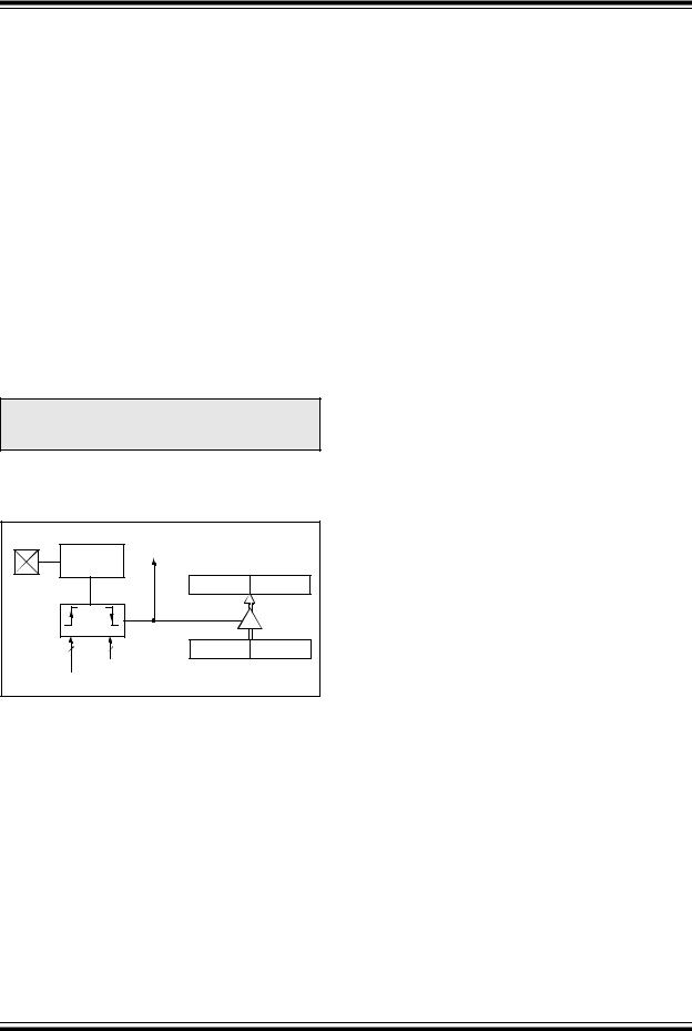
In Capture mode, CCPR1H:CCPR1L captures the 16-bit value of the TMR1 register when an event occurs on pin CCP1. An event is defined as one of the following and is configured by the CCP1M<3:0> bits of the CCP1CON register:
•Every falling edge
•Every rising edge
•Every 4th rising edge
•Every 16th rising edge
When a capture is made, the Interrupt Request Flag bit CCP1IF of the PIR1 register is set. The interrupt flag must be cleared in software. If another capture occurs before the value in the CCPR1H, CCPR1L register pair is read, the old captured value is overwritten by the new captured value (see Figure 11-1).
11.1.1CCP1 PIN CONFIGURATION
In Capture mode, the CCP1 pin should be configured as an input by setting the associated TRIS control bit.
Note: If the CCP1 pin is configured as an output, a write to the GPIO port can cause a capture condition.
FIGURE 11-1: |
CAPTURE MODE |
|
OPERATION BLOCK |
|
DIAGRAM |
|
Set Flag bit CCP1IF |
|
|
Prescaler |
|
(PIR1 register) |
|
|
|
|
|
1, 4, 16 |
|
|
|
CCP1 |
|
CCPR1H |
CCPR1L |
pin |
|
|
|
and |
|
Capture |
|
Edge Detect |
Enable |
|
|
|
|
||
|
|
TMR1H |
TMR1L |
CCP1CON<3:0> |
|
||
System Clock (FOSC) |
|
|
|
11.1.2TIMER1 MODE SELECTION
Timer1 must be running in Timer mode or Synchronized Counter mode for the CCP module to use the capture feature. In Asynchronous Counter mode, the capture operation may not work.
11.1.3SOFTWARE INTERRUPT
When the Capture mode is changed, a false capture interrupt may be generated. The user should keep the CCP1IE interrupt enable bit of the PIE1 register clear to avoid false interrupts. Additionally, the user should clear the CCP1IF interrupt flag bit of the PIR1 register following any change in operating mode.
11.1.4CCP PRESCALER
There are four prescaler settings specified by the CCP1M<3:0> bits of the CCP1CON register. Whenever the CCP module is turned off, or the CCP module is not in Capture mode, the prescaler counter is cleared. Any Reset will clear the prescaler counter.
Switching from one capture prescaler to another does not clear the prescaler and may generate a false interrupt. To avoid this unexpected operation, turn the module off by clearing the CCP1CON register before changing the prescaler (see Example 11-1).
EXAMPLE 11-1: |
CHANGING BETWEEN |
|
|
|
CAPTURE PRESCALERS |
BANKSEL CCP1CON |
;Set Bank bits to point |
|
|
|
;to CCP1CON |
CLRF |
CCP1CON |
;Turn CCP module off |
MOVLW |
NEW_CAPT_PS ;Load the W reg with |
|
|
|
; the new prescaler |
|
|
; move value and CCP ON |
MOVWF |
CCP1CON |
;Load CCP1CON with this |
|
|
; value |
|
|
|
DS41211D-page 76 |
♥ 2007 Microchip Technology Inc. |