

March 1998
74F148
8-Line to 3-Line Priority Encoder
General Description |
|
|
n Provides 3-bit binary priority code |
|||
|
|
n Input enable capability |
||||
The 'F148 provides three bits of binary coded output repre- |
||||||
n Signals when data is present on any input |
||||||
senting the position of the highest order active input, along |
||||||
n Cascadable for priority encoding of n bits |
||||||
with an output indicating the presence of any active input. It |
||||||
|
|
|||||
is easily expanded via input and output enables to provide |
|
|
||||
priority encoding over many bits. |
|
|
|
|
||
Features |
|
|
|
|
||
n Encodes eight data lines in priority |
|
|
||||
|
|
|
|
|
|
|
Ordering Code: |
|
|
|
|
||
|
|
|
|
|
|
|
|
Commercial |
Package |
|
Package Description |
|
|
|
|
Number |
|
|
|
|
|
|
|
|
|
|
|
|
74F148PC |
N16E |
|
16-Lead (0.300" Wide) Molded Dual-In-Line |
|
|
|
|
|
|
|
|
|
|
74F148SC (Note 1) |
M16A |
|
16-Lead (0.150" Wide) Molded Small Outline, JEDEC |
|
|
|
|
|
|
|
|
|
|
74F148SJ (Note 1) |
M16D |
|
16-Lead (0.300" Wide) Molded Small Outline, EIAJ |
|
|
|
|
|
|
|
|
|
Note 1: Devices also available in 13" reel. Use Suffix = SCX and SJX.
Logic Symbols
IEEE/IEC
DS009480-3
DS009480-6
Encoder Priority Line-3 to Line-8 74F148
© 1998 Fairchild Semiconductor Corporation |
DS009480 |
www.fairchildsemi.com |

Connection Diagram
Pin Assignment for SOIC and DIP
|
|
|
|
|
|
|
|
|
|
DS009480-1 |
Unit Loading/Fan Out |
|
|
||||||||
|
|
|
|
|
|
|
|
|
|
|
|
|
|
|
|
|
|
|
|
|
74F |
|
|
|
|
|
|
|
|
|
|
|
|
Pin Names |
Description |
U.L. |
Input IIH/IIL |
||||||
|
|
|
|
|
|
|
|
|
HIGH/LOW |
Output IOH/IOL |
|
I0 |
Priority Input (Active LOW) |
1.0/1.0 |
20 µA/−0.6 mA |
||||||
|
I1±I7 |
Priority Inputs (Active LOW) |
1.0/2.0 |
20 µA/−1.2 mA |
||||||
|
|
|
|
|
|
|
Enable Input (Active LOW) |
1.0/1.0 |
20 µA/−0.6 mA |
|
|
EI |
|
|
|
|
|
||||
|
|
|
|
|
|
Enable Output (Active LOW) |
50/33.3 |
−1 mA/20 mA |
||
|
EO |
|
|
|
|
|||||
|
|
|
|
|
Group Signal Output (Active LOW) |
50/33.3 |
−1 mA/20 mA |
|||
|
GS |
|
|
|
||||||
|
|
|
|
|
|
|
|
|||
|
A |
0±A |
2 |
Address Outputs (Active LOW) |
50/33.3 |
−1 mA/20 mA |
||||
Functional Description
The 'F148 8-input priority encoder accepts data from eight active LOW inputs (I0±I7) and provides a binary representation on the three active LOW outputs. A priority is assigned to each input so that when two or more inputs are simultaneously active, the input with the highest priority is represented on the output, with input line 7 having the highest priority. A HIGH on the Enable Input (EI) will force all outputs to the inactive (HIGH) state and allow new data to settle without producing erroneous information at the outputs.A Group Signal output (GS) and Enable Output (EO) are provided along with the three priority data outputs (A2, A1, A0). GS is active LOW when any input is LOW: this indicates when any input is active. EO is active LOW when all inputs are HIGH. Using the Enable Output along with the Enable Input allows cascading for priority encoding on any number of input signals. Both EO and GS are in the inactive HIGH state when the Enable Input is HIGH.
Truth Table
|
|
Inputs |
|
|
|
|
|
Outputs |
||||||
|
|
|
|
|
|
|
|
|
|
|
|
|
|
|
EI |
|
I0 I1 I2 I3 I4 I5 |
I6 |
I7 |
GS |
|
A |
0 |
A |
1 |
A |
2 |
EO |
|
H |
X X X X X X X X |
H |
H H H |
H |
||||||||||
L |
H H H H H H H H |
H |
H H H |
L |
||||||||||
L |
X X X X X X X L |
L |
L L L |
H |
||||||||||
L |
X X X X X X L |
H |
L |
H L L |
H |
|||||||||
L |
X X X X X L |
H H |
L |
L H L |
H |
|||||||||
|
|
|
|
|
|
|
|
|
|
|
|
|
||
L |
X X X X L H H H |
L |
H H L |
H |
||||||||||
L |
X X X L H H H H |
L |
L L H |
H |
||||||||||
L |
X X L H H H H H |
L |
H L H |
H |
||||||||||
L |
X L H H H H H H |
L |
L H H |
H |
||||||||||
L |
L H H H H H H H |
L |
H H H |
H |
||||||||||
|
|
|
|
|
|
|
|
|
|
|
|
|
|
|
H = HIGH Voltage Level |
|
|
|
|
|
|
|
|
|
|
|
|
||
L = LOW Voltage Level |
|
|
|
|
|
|
|
|
|
|
|
|
||
X = Immaterial |
|
|
|
|
|
|
|
|
|
|
|
|
||
www.fairchildsemi.com |
2 |
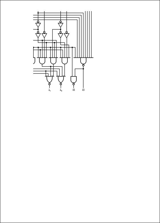
Logic Diagram
DS009480-4
Please note that this diagram is provided only for the understanding of logic operations and should not be used to estimate propagation delays.
3 |
www.fairchildsemi.com |

Absolute Maximum Ratings (Note 2)
Storage Temperature |
−65ÊC to +150ÊC |
Ambient Temperature under Bias |
−55ÊC to +125ÊC |
Junction Temperature under Bias |
−55ÊC to +175ÊC |
Plastic |
−55ÊC to +150ÊC |
VCC Pin Potential to |
|
Ground Pin |
−0.5V to +7.0V |
Input Voltage (Note 3) |
−0.5V to +7.0V |
Input Current (Note 3) |
−30 mA to +5.0 mA |
Voltage Applied to Output |
|
in HIGH State (with VCC = 0V) |
|
Standard Output |
−0.5V to V CC |
3-STATE Output |
−0.5V to +5.5V |
Current Applied to Output |
|
in LOW State (Max) |
twice the rated IOL (mA) |
Recommended Operating
Conditions
Free Air Ambient Temperature |
|
Commercial |
0ÊC to +70ÊC |
Supply Voltage |
|
Commercial |
+4.5V to +5.5V |
Note 2: Absolute maximum ratings are values beyond which the device may be damaged or have its useful life impaired. Functional operation under these conditions is not implied.
Note 3: Either voltage limit or current limit is sufficient to protect inputs.
DC Electrical Characteristics
Symbol |
Parameter |
|
|
74F |
|
Units |
VCC |
Conditions |
||||
|
|
|
|
Min |
Typ |
Max |
|
|
|
|
|
|
|
|
|
|
|
|
|
|
|
|
|
|
|
VIH |
Input HIGH Voltage |
|
|
2.0 |
|
|
V |
|
Recognized as a HIGH Signal |
|||
VIL |
Input LOW Voltage |
|
|
|
|
0.8 |
V |
|
Recognized as a LOW Signal |
|||
VCD |
Input Clamp Diode Voltage |
|
|
|
−1.2 |
V |
Min |
I IN = −18 mA |
|
|
|
|
VOH |
Output HIGH |
74F |
10% VCC |
2.5 |
|
|
V |
Min |
IOH = −1 mA |
|
|
|
|
Voltage |
74F |
5% VCC |
2.7 |
|
|
|
|
IOH = −1 mA |
|
|
|
VOL |
Output LOW |
74F |
10% VCC |
|
|
0.5 |
V |
Min |
IOL = 20 mA |
|
|
|
|
Voltage |
|
|
|
|
|
|
|
|
|
|
|
|
|
|
|
|
|
|
|
|
|
|
|
|
IIH |
Input HIGH |
74F |
|
|
|
5.0 |
µA |
Max |
VIN = 2.7V |
|
|
|
|
Current |
|
|
|
|
|
|
|
|
|
|
|
|
|
|
|
|
|
|
|
|
|
|
|
|
IBVI |
Input HIGH Current |
74F |
|
|
|
7.0 |
µA |
Max |
VIN = 7.0V |
|
|
|
|
Breakdown Test |
|
|
|
|
|
|
|
|
|
|
|
|
|
|
|
|
|
|
|
|
|
|
|
|
ICEX |
Output High |
74F |
|
|
|
50 |
µA |
Max |
VOUT = VCC |
|
|
|
|
Leakage Current |
|
|
|
|
|
|
|
|
|
|
|
|
|
|
|
|
|
|
|
|
|
|
|
|
VID |
Input Leakage |
74F |
|
4.75 |
|
|
V |
0.0 |
IID = 1.9 µA |
|
|
|
|
Test |
|
|
|
|
|
|
|
All Other Pins Grounded |
|||
|
|
|
|
|
|
|
|
|
|
|
|
|
IOD |
Output Leakage |
74F |
|
|
|
3.75 |
µA |
0.0 |
VIOD = 150 mV |
|||
|
Circuit Current |
|
|
|
|
|
|
|
All Other Pins Grounded |
|||
|
|
|
|
|
|
|
|
|
|
|
|
|
IIL |
|
|
|
|
|
|
|
|
V IN = 0.5V |
|
|
|
Input LOW |
|
|
|
|
−0.6 |
mA |
Max |
(I0, |
EI) |
|||
|
Current |
|
|
|
|
−1.2 |
mA |
|
V IN = 0.5V |
(I1±I7) |
||
IOS |
Output Short-Circuit Current |
|
−60 |
|
−150 |
mA |
Max |
V OUT = 0V |
|
|
|
|
ICCH |
Power Supply Current |
|
|
|
|
35 |
mA |
Max |
VO = HIGH |
|
|
|
ICCL |
Power Supply Current |
|
|
|
|
35 |
mA |
Max |
VO = LOW |
|
|
|
www.fairchildsemi.com |
4 |

Application
16-Input Priority Encoder
|
|
|
|
|
|
|
|
|
|
|
|
|
DS009480-5 |
|
|
AC Electrical Characteristics |
|
|
|
|
|
||||||||||
|
|
|
|
|
|
|
|
|
|
|
|
|
|
|
|
|
|
|
|
|
|
|
|
|
|
|
74F |
|
74F |
|
|
|
|
|
|
|
|
|
|
|
|
|
|
|
|
|
|
|
|
|
|
|
|
|
|
|
|
|
TA = +25ÊC |
|
TA, VCC = Com |
|
|
Symbol |
|
|
|
|
Parameter |
|
VCC = +5.0V |
|
CL = 50 pF |
Units |
|||||
|
|
|
|
|
|
|
|
|
|
|
CL = 50 pF |
|
|
|
|
|
|
|
|
|
|
|
|
|
|
Min |
Typ |
Max |
Min |
Max |
|
|
|
|
|
|
|
|
|
|
|
|
|
|
|
|
|
tPLH |
|
Propagation Delay |
3.0 |
7.0 |
9.0 |
3.0 |
10.0 |
ns |
|||||||
tPHL |
|
In to |
A |
n |
3.0 |
8.0 |
10.5 |
3.0 |
12.0 |
|
|||||
tPLH |
|
Propagation Delay |
2.5 |
5.0 |
6.5 |
2.5 |
7.5 |
ns |
|||||||
tPHL |
|
In to |
EO |
|
|
2.5 |
5.5 |
7.5 |
2.5 |
8.5 |
|
||||
tPLH |
|
Propagation Delay |
2.5 |
7.0 |
9.0 |
2.5 |
10.0 |
ns |
|||||||
tPHL |
|
In to |
GS |
|
|
2.5 |
6.0 |
8.0 |
2.5 |
9.0 |
|
||||
tPLH |
|
Propagation Delay |
2.5 |
6.5 |
8.5 |
2.5 |
9.5 |
ns |
|||||||
tPHL |
|
EI |
to |
A |
n |
2.5 |
6.0 |
8.0 |
2.5 |
9.0 |
|
||||
tPLH |
|
Propagation Delay |
2.5 |
5.0 |
7.0 |
2.5 |
8.0 |
ns |
|||||||
tPHL |
|
EI |
to |
GS |
|
2.5 |
6.0 |
7.5 |
2.5 |
8.5 |
|
||||
tPLH |
|
Propagation Delay |
2.5 |
5.5 |
7.0 |
2.5 |
8.0 |
ns |
|||||||
tPHL |
|
EI |
to |
EO |
|
3.0 |
8.0 |
10.5 |
3.0 |
12.0 |
|
||||
5 |
www.fairchildsemi.com |
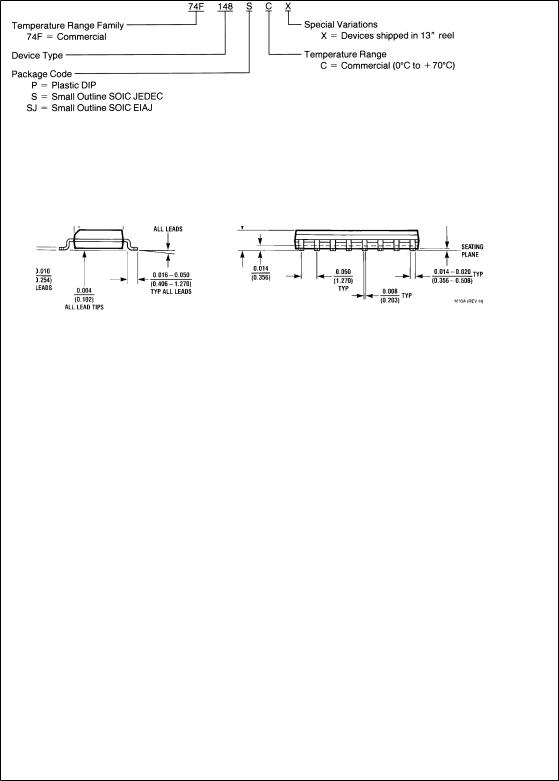
Ordering Information
The device number is used to form part of a simplified purchasing code where the package type and temperature range are defined as follows:
DS009480-7
Physical Dimensions inches (millimeters) unless otherwise noted
16-Lead (0.150" Wide) Molded Small Outline Package, JEDEC (S)
Package Number M16A
www.fairchildsemi.com |
6 |
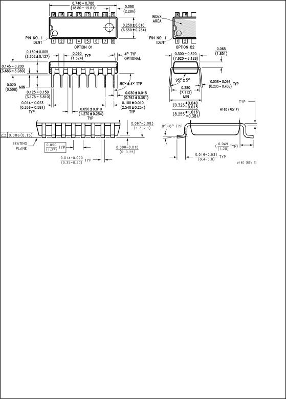
Physical Dimensions inches (millimeters) unless otherwise noted (Continued)
16-Lead (0.150" Wide) Molded Small Outline Package, EIAJ (SJ)
Package Number M16D
16-Lead (0.300" Wide) Molded Dual-In-Line Package (P)
Package Number N16E
7 |
www.fairchildsemi.com |

74F148 8-Line to 3-Line Priority Encoder
LIFE SUPPORT POLICY
FAIRCHILD'S PRODUCTS ARE NOT AUTHORIZED FOR USE AS CRITICAL COMPONENTS IN LIFE SUPPORT DEVICES OR SYSTEMS WITHOUT THE EXPRESS WRITTEN APPROVAL OF THE PRESIDENT OF FAIRCHILD SEMICONDUCTOR CORPORATION. As used herein:
1. Life support devices or systems are devices or sys- |
2. A critical component in any component of a life support |
tems which, (a) are intended for surgical implant into |
device or system whose failure to perform can be rea- |
the body, or (b) support or sustain life, and (c) whose |
sonably expected to cause the failure of the life support |
failure to perform when properly used in accordance |
device or system, or to affect its safety or effectiveness. |
with instructions for use provided in the labeling, can |
|
be reasonably expected to result in a significant injury |
|
to the user.
Fairchild Semiconductor |
Fairchild Semiconductor |
Fairchild Semiconductor |
National Semiconductor |
||
Corporation |
Europe |
|
|
Hong Kong Ltd. |
Japan Ltd. |
Americas |
|
Fax: |
+49 (0) 1 80-530 85 86 |
13th Floor, Straight Block, |
Tel: 81-3-5620-6175 |
Customer Response Center |
Email: europe.support@nsc.com |
Ocean Centre, 5 Canton Rd. |
Fax: 81-3-5620-6179 |
||
Tel: 1-888-522-5372 |
Deutsch |
Tel: |
+49 (0) 8 141-35-0 |
Tsimshatsui, Kowloon |
|
|
English |
Tel: |
+44 (0) 1 793-85-68-56 |
Hong Kong |
|
|
Italy |
Tel: |
+39 (0) 2 57 5631 |
Tel: +852 2737-7200 |
|
www.fairchildsemi.com |
|
|
|
Fax: +852 2314-0061 |
|
Fairchild does not assume any responsibility for use of any circuitry described, no circuit patent licenses are implied and Fairchild reserves the right at any time without notice to change said circuitry and specifications.