

Denisov A. K., group 3205
Task №1 Diodes with positive dynamic resistance
Calculate the maximum value of rectified current for a DD with the ideality factor
 and microwave power
 .
.Estimate tangential sensivity (express in dBm), effective diode noise temperature is
 ,
amplification band
,
amplification band
 .
.Characterize similarities and differences in functional role, structure, parameters between microwave DD, VD, MD and PIN-diodes.
Find «standard» circuit models of microwave DD and MD, using available information sources such as the Internet, lectures, MicrowaveOffice etc.
Given:
 ;
;
 ;
;
 ;
;
 .
.
Find:
1. (for DD)
2.
 (for
DD)
(for
DD)
3. Similarities and differences between DD, VD, and PIN-diodes
4. Circuit models of microwave DD and MD
Solution:
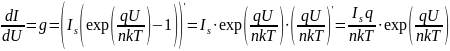
1. Current sensivity:
 ,
,
 – max
rectified diode current;
– max
rectified diode current;
 – microwave
power.
– microwave
power.

equivalent circuit of DD
Also,
 ,
,
 -
voltage-current characteristic curve,
-
voltage-current characteristic curve,
g - differential conductivity,
 -
frequency limit,
-
frequency limit,
 ,
,
 - parameters of contacts and rectifier junction
Supposing
the resistance of the ohmic contact to be much less than the
resistance of the rectifier junction, we get
 .
Also, the device is working in the frequency bandwidth, so
.
Also, the device is working in the frequency bandwidth, so
 .
.
Then:
 .
According to this, we get the following expression:
.
According to this, we get the following expression:

Values of curve and differential conductivity at the operation point can be evaluated using the expression for VCC:
 ,
,
 –saturation
current;
–saturation
current;
 –diode
voltage;
–diode
voltage;
q–electron charge;
n – ideality factor;
k – Stefan-Boltzmann constant;
T –temperature.
We need to differentiate the VCC once to find the value of differential conductivity and twice to find the curve:

After that we get:

Then:


Supposing the temperature T=300 K:

2. To estimate the tangential sensivity we use the following expression:

 -
minimum value of noise power.
-
minimum value of noise power.
Using the expression for Nyquist noise:

And considering:
 ;
;

We get this:


 dBm
dBm
Answer:
1.

3. 1. Detector diode
Function:
converts
energetically weak microwave signals ( )
W into DC
signal.
It uses rectifying properties of a diode for separation
of a low-frequency signal from an amplitude modulated microwave
oscillation, which is then used as an input of an amplifier.
Detector
diode is used as an indicator (detector) of weak signals.
)
W into DC
signal.
It uses rectifying properties of a diode for separation
of a low-frequency signal from an amplitude modulated microwave
oscillation, which is then used as an input of an amplifier.
Detector
diode is used as an indicator (detector) of weak signals.
Structure: there are two kinds of structure:
point-contact diode (a pointed metal wire is placed in contact with an n-type semiconductor, usually Si or Ge) (1)
p
 lanar
diode (epitaxial structure with an evaporated metal film) (2)
lanar
diode (epitaxial structure with an evaporated metal film) (2)Schottky-barrier junction is usually used
P
(1)
arameters:VCC

Current sensibility
Tangential sensibility
N
 oise
quotient
oise
quotient

F
(2)
requency limit
Impedance

Specialty: microwave signal is distorted according to the VCC. Most of modern detector diodes are epitaxial structures made of GaAs. High-speed response is provided by using of high-concentration doping and small-area contacts as well as using materials with high charge-carrier mobility.
2. Mixer diode
Function: mixer diode is used for transduction of a microwave signal to a signal of lower frequency, it is caused by the non-linear VCC. Usually used as heterodynes, microwave mixers, sometimes also used as precise detectors (microwave power 10-12 W).
Structure: usually similar to a detector diode structure. To provide a high frequency limit, mixer diodes can have different complex shapes (for example, a cross shape of a mixer diode with SB).


Mixer diode structure
Parameters:
VCC
Noise quotient
Frequency limit
Impedance
Specialty: mixer diode has a high sensibility to microwave signal, it means that sometimes even a low-level signal can cause a junction breakdown or a structure burn. That is why low-concentration doped materials should be used, e.g. GaAs.

Vcc of detector and mixer diodes
3. Varactor diodes
Function: varactor diode is used as voltage-controlled capacitors. The principle is dependence of capacity of a reversed-biased p-n junction on voltage. Barrier capacity is dependent on the thickness of the depletion zone. They are commonly used in voltage-controlled oscillators, parametric amplifiers, and frequency multipliers. Voltage-controlled oscillators have many applications such as frequency modulation for FM transmitters and phase-locked loops. Phase-locked loops are used for the frequency synthesizers that tune many radios, television sets, and cellular telephones.
Structure: The varactor diode consists of a standard p-n junction, although it is obviously optimised for its function as a variable capacitor. Some varactor diodes may be referred to as abrupt, hyperabrupt, or super hyper abrupt. These refer to the change in junction capacitance with changing reverse bias as being abrupt or hyper-abrupt, or super hyperabrupt. These diodes offer a relatively large change in capacitance. Planar structures are commonly used.

Varactor diode structure
Parameters:
Barrier capacity (voltage-capacitance characteristic)

Zero-biased capacitance

Overlap coefficient

Quality factor

Cut-off frequency (Q = 1)

Specialty: there is no diffusion capacitance when reverse bias is applied. Inside of microwave range GaAs is used instead of Si because of its low Rs, high carrier-mobility and cut-off frequency.

Voltage-capacitance characteristic
4. PIN diode
Function: PIN diodes are useful as RF switches, attenuators, photodetectors, and phase shifters. At high frequencies, the PIN diode appears as a resistor whose resistance is an inverse function of its forward current. Consequently, PIN diode can be used in some variable attenuator designs as amplitude modulators or output leveling circuits. PIN diodes are sometimes used as input protection devices for high frequency test probes. If the input signal is within range, the PIN diode has little impact as a small capacitance. If the signal is large, then the PIN diode starts to conduct and becomes a resistor that shunts most of the signal to ground (limiter).
Structure: a wide, undoped intrinsic semiconductor region between a p-type semiconductor and an n-type semiconductor region. The p-type and n-type regions are typically heavily doped because they are used for ohmic contacts.

PIN diode structure
Parameters:
VCC
Transmission loss

Quality coefficient

Frequency limit ;

response time

Specialty: A PIN diode obeys the standard diode equation for low frequency signals. At higher frequencies, the diode looks like an almost perfect (very linear, even for large signals) resistor. There is a lot of stored charge in the intrinsic region. At low frequencies, the charge can be removed and the diode turns off. At higher frequencies, there is not enough time to remove the charge, so the diode never turns off. In a PIN diode, the depletion region exists almost completely within the intrinsic region. This depletion region is much larger than in a PN diode, and almost constant-size, independent of the reverse bias applied to the diode. It also means a high breakdown voltage.
