

Дьяконов / Datasheets / MAX11044-MAX11056
.pdfEVALUATION KIT AVAILABLE
MAX11044/MAX11045/MAX11046/
MAX11054/MAX11055/MAX11056
4-/6-/8-Channel, 16-/14-Bit, Simultaneous-Sampling ADCs
General Description
The MAX11044/MAX11045/MAX11046 16-bit and MAX11054/MAX11055/MAX11056 14-bit ADCs offer 4, 6, or 8 independent input channels. Featuring independent track and hold (T/H) and SAR circuitry, these parts provide simultaneous sampling at 250ksps for each channel.
The MAX11044/MAX11045/MAX11046 and MAX11054/ MAX11055/MAX11056 accept a ±5V input. All inputs are overrange protected with internal ±20mA input clamps providing overrange protection with a simple external resistor. Other features include a 4MHz T/H input bandwidth, internal clock, and internal or external reference. A 20MHz, bidirectional, parallel interface provides the conversion results and accepts digital configuration inputs.
The MAX11044/MAX11045/MAX11046 and MAX11054/ MAX11055/MAX11056 operate with a 4.75V to 5.25V analog supply and a separate flexible 2.7V to 5.25V digital supply for interfacing with the host without a level shifter. The MAX11044/MAX11045/MAX11046 are available in a 56-pin TQFN and 64-pin TQFP packages while the MAX11054/MAX11055/MAX11056 are available in TQFP only and operate over the extended -40°C to +85°C temperature range.
Applications
Automatic Test Equipment
Power-Factor Monitoring and Correction
Power-Grid Protection
Multiphase Motor Control
Vibration and Waveform Analysis
Functional Diagram
AVDD |
|
|
|
DVDD |
CH0 |
|
|
|
DB15** |
S/H |
16-/14-BIT ADC |
|
|
|
CLAMP |
|
|
||
|
|
8x16-/14-BITREGISTERS |
BIDIRECTIONALDRIVERS |
DB4 |
|
|
DB3/CR3 |
||
CH7† |
S/H |
DB0/CR0 |
||
CLAMP |
16-/14-BIT ADC |
|
|
|
AGNDS |
|
CONFIGURATION |
WR |
|
|
|
REGISTERS |
RD |
|
|
|
|
|
|
|
|
|
INTERFACE |
CS |
|
|
|
CONVST |
|
|
|
|
AND |
|
AGND |
|
|
SHDN |
|
|
|
CONTROL |
||
|
|
|
EOC |
|
MAX11044/MAX11045/MAX11046/ |
|
|||
MAX11054/MAX11055/MAX11056 |
|
|
||
|
|
INT REF |
|
DGND |
|
10kΩ |
|
|
|
BANDGAP |
REF |
|
RDC |
|
|
|
|||
REFERENCE |
|
BUF |
|
|
REFIO |
|
EXT REF |
|
RDC_SENSE* |
*CONNECTED INTERNALLY TO RDC ON THE TQFN PARTS |
**MAX11044/MAX11045/MAX11046 |
|||
†MAX11046/MAX11056 |
|
|||
Features
♦16-Bit ADC (MAX11044/MAX11045/MAX11046) and
14-Bit ADC (MAX11054/MAX11055/MAX11056)
8-Channel ADC (MAX11046/MAX11056)
6-Channel ADC (MAX11045/MAX11055)
4-Channel ADC (MAX11044/MAX11054)
♦Single Analog and Digital Supply
♦High-Impedance Inputs Up to 1GΩ
♦On-Chip T/H Circuit for Each Channel
♦Fast 3µs Conversion Time
♦High Throughput: 250ksps for Each Channel
♦16-Bit/14-Bit, High-Speed, Parallel Interface
♦Internal Clocked Conversions
♦10ns Aperture Delay
♦100ps Channel-to-Channel T/H Matching
♦Low Drift, Accurate 4.096V Internal Reference Providing an Input Range of ±5V
♦External Reference Range of 3.0V to 4.25V, Allowing Full-Scale Input Ranges of ±4.0V to ±5.2V
♦56-Pin (8mm x 8mm) TQFN and 64-Pin (10mm x 10mm) TQFP Packages
♦Evaluation Kit Available
Ordering Information
PART |
PIN-PACKAGE |
CHANNELS |
|
|
|
MAX11044ETN+ |
56 TQFN-EP* |
4 |
MAX11044ECB+ |
64 TQFP-EP* |
4 |
|
|
|
MAX11045ETN+ |
56 TQFN-EP* |
6 |
|
|
|
MAX11045ECB+ |
64 TQFP-EP* |
6 |
|
|
|
MAX11046ETN+ |
56 TQFN-EP* |
8 |
MAX11046ECB+ |
64 TQFP-EP* |
8 |
MAX11054ECB+ |
64 TQFP-EP* |
4 |
|
|
|
MAX11055ECB+ |
64 TQFP-EP* |
6 |
MAX11056ECB+ |
64 TQFP-EP* |
8 |
Note: All devices are specified over the -40°C to +85°C operating temperature range.
+Denotes a lead(Pb)-free/RoHS-compliant package. *EP = Exposed pad.
Pin Configurations appear at end of data sheet.
For pricing, delivery, and ordering information, please contact Maxim Direct at 1-888-629-4642, or visit Maxim’s website at www.maximintegrated.com.
19-5036; Rev 5; 1/11
MAX11044/MAX11045/MAX11046/
MAX11054/MAX11055/MAX11056
4-/6-/8-Channel, 16-/14-Bit, Simultaneous-Sampling ADCs
ABSOLUTE MAXIMUM RATINGS
AVDD to AGND ........................................................ |
-0.3V to +6V |
Maximum Current into Any Pin Except AVDD, DVDD, AGND, |
||
DVDD to AGND and DGND ..................................... |
-0.3V to +6V |
DGND ........................................................................... |
|
±50mA |
DGND to AGND..................................................... |
-0.3V to +0.3V |
Continuous Power Dissipation |
|
|
AGNDS to AGND................................................... |
-0.3V to +0.3V |
56-Pin TQFN (derate 47.6mW/°C above +70°C) .... |
3809.5mW |
|
CH0–CH7 to AGND ............................................... |
-7.5V to +7.5V |
64-Pin TQFP (derate 43.5mW/°C above +70°C)........ |
3478mW |
|
REFIO, RDC to AGND .................................. |
-0.3V to the lower of |
Operating Temperature Range ........................... |
-40°C to +85°C |
|
EOC, WR, RD, CS, CONVST to AGND |
(VAVDD + 0.3V) and +6V |
Junction Temperature ...................................................... |
|
+150°C |
-0.3V to the lower of |
Storage Temperature Range ............................. |
-65°C to +150°C |
||
|
(VDVDD + 0.3V) and +6V |
Lead Temperature (soldering, 10s) ................................. |
|
+300°C |
DB0–DB15 to AGND .................................... |
-0.3V to the lower of |
Soldering Temperature (reflow) ....................................... |
|
+260°C |
(VDVDD + 0.3V) and +6V
Stresses beyond those listed under “Absolute Maximum Ratings” may cause permanent damage to the device. These are stress ratings only, and functional operation of the device at these or any other conditions beyond those indicated in the operational sections of the specifications is not implied. Exposure to absolute maximum rating conditions for extended periods may affect device reliability.
ELECTRICAL CHARACTERISTICS
(VAVDD = +4.75V to +5.25V, VDVDD = +2.70V to +5.25V, VAGNDS = VAGND = VDGND = 0V, VREFIO = internal reference, CRDC = 4 x 33µF, CREFIO = 0.1µF, CAVDD = 4 x 0.1µF || 10µF, CDVDD = 3 x 0.1µF || 10µF; all digital inputs at DVDD or DGND, unless otherwise noted, fSAMPLE = 250ksps. TA = -40°C to +85°C, unless otherwise noted. Typical values are at TA = +25°C.)
PARAMETER |
SYMBOL |
CONDITIONS |
MIN |
TYP |
MAX |
UNITS |
||
|
|
|
|
|
|
|
|
|
STATIC PERFORMANCE (Note 1) |
|
|
|
|
|
|
|
|
|
|
|
|
|
|
|
|
|
Resolution |
N |
MAX11044/MAX11045/MAX11046 |
16 |
|
|
Bits |
||
MAX11054/MAX11055/MAX11056 |
14 |
|
|
|||||
|
|
|
|
|
||||
|
|
|
|
|
|
|
|
|
Integral Nonlinearity |
INL |
MAX11044/MAX11045/MAX11046 |
> -2 |
±0.4 |
< +2 |
LSB |
||
MAX11054/MAX11055/MAX11056 |
-0.8 |
±0.13 |
+0.8 |
|||||
|
|
|
||||||
Differential Nonlinearity |
DNL |
MAX11044/MAX11045/MAX11046 |
> -1 |
±0.4 |
< +1.2 |
LSB |
||
MAX11054/MAX11055/MAX11056 |
-0.6 |
±0.15 |
+0.6 |
|||||
|
|
|
||||||
No Missing Codes |
|
MAX11044/MAX11045/MAX11046 |
16 |
|
|
Bits |
||
|
MAX11054/MAX11055/MAX11056 |
14 |
|
|
||||
|
|
|
|
|
||||
|
|
|
|
|
|
|
|
|
Offset Error |
|
|
|
|
±0.001 |
±0.015 |
%FSR |
|
|
|
|
|
|
|
|
|
|
Channel Offset Matching |
|
|
|
|
±0.001 |
±0.015 |
%FSR |
|
|
|
|
|
|
|
|
|
|
Offset Temperature Coefficient |
|
|
|
|
±0.8 |
|
µV/°C |
|
Gain Error |
|
|
|
|
|
±0.015 |
%FSR |
|
|
|
|
|
|
|
|
|
|
Positive Full-Scale Error |
|
|
|
|
|
±0.015 |
%FSR |
|
|
|
|
|
|
|
|
|
|
Negative Full-Scale Error |
|
|
|
|
|
±0.015 |
%FSR |
|
|
|
|
|
|
|
|
|
|
Positive Full-Scale Error Matching |
|
|
|
|
|
±0.01 |
%FSR |
|
|
|
|
|
|
|
|
|
|
Negative Full-Scale Error Matching |
|
|
|
|
|
±0.01 |
%FSR |
|
Channel Gain-Error Matching |
|
Between all channels |
|
|
±0.01 |
%FSR |
||
|
|
|
|
|
|
|
|
|
Gain Temperature Coefficient |
|
|
|
|
±0.5 |
|
ppm/°C |
|
|
|
|
|
|
|
|
|
|
DYNAMIC PERFORMANCE |
|
|
|
|
|
|
|
|
|
|
|
|
|
|
|
|
|
|
|
|
MAX11044/MAX11045/ |
91 |
92.3 |
|
|
|
|
|
fIN = 10kHz, |
MAX11046 |
|
|
|||
Signal-to-Noise Ratio |
SNR |
|
|
|
dB |
|||
|
|
|
|
|||||
full-scale input |
MAX11054/MAX11055/ |
84.5 |
85.2 |
|
||||
|
|
|
|
|||||
|
|
|
|
|
||||
|
|
|
MAX11056 |
|
|
|||
|
|
|
|
|
|
|
||
|
|
|
|
|
|
|
|
|
|
|
|
MAX11044/MAX11045/ |
90.5 |
92 |
|
|
|
Signal-to-Noise and Distortion |
|
fIN = 10kHz, |
MAX11046 |
|
|
|||
SINAD |
|
|
|
dB |
||||
|
|
|
|
|||||
Ratio |
full-scale input |
MAX11054/MAX11055/ |
84.5 |
85.2 |
|
|||
|
|
|
||||||
|
|
|
|
|
||||
|
|
|
MAX11056 |
|
|
|||
|
|
|
|
|
|
|
||
|
|
|
|
|
|
|
|
|
|
|
|
|
|
|
|
|
|
2 |
Maxim Integrated |

MAX11044/MAX11045/MAX11046/
MAX11054/MAX11055/MAX11056
4-/6-/8-Channel, 16-/14-Bit, Simultaneous-Sampling ADCs
ELECTRICAL CHARACTERISTICS (continued)
(VAVDD = +4.75V to +5.25V, VDVDD = +2.70V to +5.25V, VAGNDS = VAGND = VDGND = 0V, VREFIO = internal reference, CRDC = 4 x 33µF, CREFIO = 0.1µF, CAVDD = 4 x 0.1µF || 10µF, CDVDD = 3 x 0.1µF || 10µF; all digital inputs at DVDD or DGND, unless otherwise noted, fSAMPLE = 250ksps. TA = -40°C to +85°C, unless otherwise noted. Typical values are at TA = +25°C.)
PARAMETER |
SYMBOL |
CONDITIONS |
MIN |
TYP |
MAX |
UNITS |
|||
|
|
|
|
|
|
|
|
|
|
|
|
|
|
|
MAX11044/MAX11045/ |
98 |
104 |
|
|
|
|
|
|
fIN = 10kHz, |
MAX11046 |
|
|
||
Spurious-Free Dynamic Range |
SFDR |
|
|
|
dB |
||||
|
|
|
|
||||||
full-scale input |
MAX11054/MAX11055/ |
95 |
104 |
|
|||||
|
|
|
|
|
|
||||
|
|
|
|
|
|
|
|||
|
|
|
|
|
MAX11056 |
|
|
||
|
|
|
|
|
|
|
|
|
|
|
|
|
|
|
|
|
|
|
|
|
|
|
|
|
MAX11044/MAX11045/ |
|
-105 |
-98 |
|
|
|
|
|
fIN = 10kHz, |
MAX11046 |
|
|
||
Total Harmonic Distortion |
THD |
|
|
|
dB |
||||
|
|
|
|
||||||
full-scale input |
MAX11054/MAX11055/ |
|
-104 |
-95 |
|||||
|
|
|
|
|
|
||||
|
|
|
|
|
|
|
|||
|
|
|
|
|
MAX11056 |
|
|
||
|
|
|
|
|
|
|
|
|
|
|
|
|
|
|
|
|
|
|
|
Channel-to-Channel Crosstalk |
|
fIN = 60Hz, full scale and ground on |
|
-126 |
-100 |
dB |
|||
|
adjacent channel (Note 2) |
|
|||||||
|
|
|
|
|
|
|
|
||
|
|
|
|
|
|
|
|
|
|
ANALOG INPUTS (CH0–CH7) |
|
|
|
|
|
|
|
||
|
|
|
|
|
|
|
|
|
|
Input Voltage Range |
|
|
(Note 3) |
|
|
|
±1.22 x |
V |
|
|
|
|
|
|
VREFIO |
||||
|
|
|
|
|
|
|
|
|
|
|
|
|
|
|
|
|
|
|
|
Input Leakage Current |
|
|
|
|
-1 |
|
+1 |
µA |
|
Input Capacitance |
|
|
|
|
|
15 |
|
pF |
|
|
|
|
|
|
|
|
|
|
|
Input-Clamp Protection Current |
|
|
Each input simultaneously |
-20 |
|
+20 |
mA |
||
|
|
|
|
|
|
|
|
|
|
TRACK AND HOLD |
|
|
|
|
|
|
|
||
|
|
|
|
|
|
|
|
|
|
Throughput Rate |
|
|
|
Per channel |
|
1 |
|
250 |
ksps |
|
|
|
|
|
|
|
|
|
|
Acquisition Time |
|
tACQ |
|
|
1 |
|
1000 |
µs |
|
Full-Power Bandwidth |
|
|
-3dB point |
|
|
4 |
|
MHz |
|
|
|
-0.1dB point |
|
|
> 0.2 |
|
|||
|
|
|
|
|
|
|
|
||
|
|
|
|
|
|
|
|
|
|
Aperture Delay |
|
|
|
|
|
10 |
|
ns |
|
|
|
|
|
|
|
|
|
|
|
Aperture-Delay Matching |
|
|
|
|
|
100 |
|
ps |
|
|
|
|
|
|
|
|
|
|
|
Aperture Jitter |
|
|
|
|
|
|
50 |
|
psRMS |
INTERNAL REFERENCE |
|
|
|
|
|
|
|
||
|
|
|
|
|
|
|
|
||
REFIO Voltage |
|
VREF |
|
|
4.08 |
4.096 |
4.112 |
V |
|
REFIO Temperature Coefficient |
|
|
|
|
|
±5 |
|
ppm/°C |
|
EXTERNAL REFERENCE |
|
|
|
|
|
|
|
||
Input Current |
|
|
|
|
|
-10 |
|
+10 |
µA |
|
|
|
|
|
|
|
|
|
|
REF Voltage-Input Range |
|
VREF |
|
|
3.00 |
|
4.25 |
V |
|
REF Input Capacitance |
|
|
|
|
|
15 |
|
pF |
|
|
|
|
|
|
|
|
|
||
DIGITAL INPUTS (CR0–CR3, RD, WR, CS, CONVST) |
|
|
|
|
|
||||
|
|
|
|
|
|
|
|||
Input Voltage High |
|
VIH |
VDVDD = 2.7V to 5.25V |
2 |
|
|
V |
||
Input Voltage Low |
|
VIL |
VDVDD = 2.7V to 5.25V |
|
|
0.8 |
V |
||
Input Capacitance |
|
CIN |
|
|
|
10 |
|
pF |
|
Input Current |
|
IIN |
VIN = 0V or VDVDD |
|
|
±10 |
µA |
||
|
|
|
|
|
|
|
|
|
|
Maxim Integrated |
3 |

MAX11044/MAX11045/MAX11046/
MAX11054/MAX11055/MAX11056
4-/6-/8-Channel, 16-/14-Bit, Simultaneous-Sampling ADCs
ELECTRICAL CHARACTERISTICS (continued)
(VAVDD = +4.75V to +5.25V, VDVDD = +2.70V to +5.25V, VAGNDS = VAGND = VDGND = 0V, VREFIO = internal reference, CRDC = 4 x 33µF, CREFIO = 0.1µF, CAVDD = 4 x 0.1µF || 10µF, CDVDD = 3 x 0.1µF || 10µF; all digital inputs at DVDD or DGND, unless otherwise noted, fSAMPLE = 250ksps. TA = -40°C to +85°C, unless otherwise noted. Typical values are at TA = +25°C.)
PARAMETER |
|
SYMBOL |
|
|
CONDITIONS |
MIN |
TYP |
MAX |
UNITS |
|
DIGITAL OUTPUTS (DB0–DB15, EOC) |
|
|
|
|
|
|
|
|
||
Output Voltage High |
|
VOH |
|
ISOURCE = 1.2mA |
VDVDD - |
|
|
V |
||
|
|
0.4 |
|
|
||||||
|
|
|
|
|
|
|
|
|
|
|
|
|
|
|
|
|
|
|
|
|
|
Output Voltage Low |
|
VOL |
|
ISINK = 1mA |
|
|
|
0.25 |
0.4 |
V |
Three-State Leakage Current |
|
|
|
DB0–DB15, VRD ≥ VIH or VCS ≥ VIH |
|
|
10 |
µA |
||
Three-State Output Capacitance |
|
|
|
DB0–DB15, VRD ≥ VIH or VCS ≥ VIH |
|
15 |
|
pF |
||
Analog Supply Voltage |
|
AVDD |
|
|
|
|
4.75 |
|
5.25 |
V |
|
|
|
|
|
|
|
|
|
|
|
Digital Supply Voltage |
|
DVDD |
|
|
|
|
2.70 |
|
5.25 |
V |
|
|
|
|
MAX11046/MAX11056, VAVDD = 5V |
|
|
48 |
|
||
Analog Supply Current |
|
IAVDD |
|
MAX11045/MAX11055, VAVDD = 5V |
|
|
39 |
mA |
||
|
|
|
|
MAX11044/MAX11054, VAVDD = 5V |
|
|
30 |
|
||
|
|
|
|
MAX11046/MAX11056, VDVDD = 3.3V |
|
|
7.0 |
|
||
Digital Supply Current (Note 9) |
|
IDVDD |
|
MAX11045/MAX11055, VDVDD = 3.3V |
|
|
6.5 |
mA |
||
|
|
|
|
MAX11044/MAX11054, VDVDD = 3.3V |
|
|
5.5 |
|
||
Shutdown Current |
|
IDVDD |
|
|
|
|
|
|
10 |
µA |
|
IAVDD |
|
|
|
|
|
|
10 |
||
|
|
|
|
|
|
|
|
|
||
|
|
|
|
VAVDD = 4.9V |
MAX11044/MAX11045/ |
|
±1 |
|
|
|
|
|
|
|
MAX11046 |
|
|
|
|||
|
|
|
|
|
|
|
|
|||
Power-Supply Rejection |
|
PSR |
|
to 5.1V |
|
|
|
|
|
LSB |
|
|
|
MAX11054/MAX11055/ |
|
|
|
||||
|
|
|
|
(Note 5) |
|
|
±0.25 |
|
|
|
|
|
|
|
|
MAX11056 |
|
|
|
||
|
|
|
|
|
|
|
|
|
|
|
|
|
|
|
|
|
|
|
|
|
|
TIMING CHARACTERISTICS (Note 4) |
|
|
|
|
|
|
|
|
|
|
CONVST Rise to EOC |
|
tCON |
|
Conversion time (Note 6) |
|
|
3 |
µs |
||
Acquisition Time |
|
tACQ |
|
|
|
|
1 |
|
1000 |
µs |
CS Rise to CONVST Rise |
|
tQ |
|
Sample quiet time (Note 6) |
500 |
|
|
ns |
||
CONVST Rise to EOC Rise |
|
t0 |
|
|
|
|
|
47 |
140 |
ns |
EOC Fall to CONVST Fall |
|
t1 |
|
CONVST mode B0 = 0 only (Note 7) |
0 |
|
|
ns |
||
CONVST Low Time |
|
t2 |
|
CONVST mode B0 = 1 only |
20 |
|
|
ns |
||
CS Fall to WR Fall |
|
t3 |
|
|
|
|
0 |
|
|
ns |
WR Low Time |
|
t4 |
|
|
|
|
20 |
|
|
ns |
CS Rise to WR Rise |
|
t5 |
|
|
|
|
0 |
|
|
ns |
Input Data Setup Time |
|
t6 |
|
|
|
|
10 |
|
|
ns |
Input Data Hold Time |
|
t7 |
|
|
|
|
1 |
|
|
ns |
CS Fall to RD Fall |
|
t8 |
|
|
|
|
0 |
|
|
ns |
RD Low Time |
|
t9 |
|
|
|
|
30 |
|
|
ns |
|
|
|
|
|
|
|
|
|
|
|
4 |
Maxim Integrated |

MAX11044/MAX11045/MAX11046/
MAX11054/MAX11055/MAX11056
4-/6-/8-Channel, 16-/14-Bit, Simultaneous-Sampling ADCs
ELECTRICAL CHARACTERISTICS (continued)
(VAVDD = +4.75V to +5.25V, VDVDD = +2.70V to +5.25V, VAGNDS = VAGND = VDGND = 0V, VREFIO = internal reference, CRDC = 4 x 33µF, CREFIO = 0.1µF, CAVDD = 4 x 0.1µF || 10µF, CDVDD = 3 x 0.1µF || 10µF; all digital inputs at DVDD or DGND, unless otherwise noted, fSAMPLE = 250ksps. TA = -40°C to +85°C, unless otherwise noted. Typical values are at TA = +25°C.)
PARAMETER |
SYMBOL |
CONDITIONS |
MIN |
TYP |
MAX |
UNITS |
|
|
|
|
|
|
|
RD Rise to CS Rise |
t10 |
|
0 |
|
|
ns |
RD High Time |
t11 |
|
10 |
|
|
ns |
RD Fall to Data Valid |
t12 |
|
|
|
35 |
ns |
RD Rise to Data Hold Time |
t13 |
(Note 7) |
5 |
|
|
ns |
|
|
|
|
|
|
|
Note 1: See the Definitions section at the end of the data sheet.
Note 2: Tested with alternating channels modulated at full scale and ground. Note 3: See the Input Range and Protection section for more details.
Note 4: CLOAD = 30pF on DB0–DB15 and EOC. Inputs (CH0–CH7) alternate between full scale and zero scale. fCONV = 250ksps. All data is read out.
Note 5: Defined as the change in positive full scale caused by a ±2% variation in the nominal supply voltage. Note 6: It is recommended that RD, WR, and CS are kept high for the quiet time (tQ) and conversion time (tCON). Note 7: Guaranteed by design.
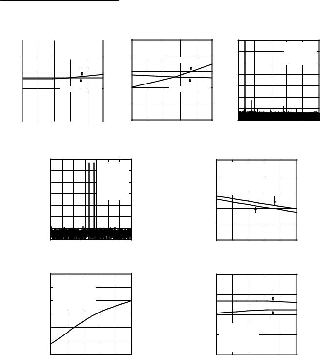
Typical Operating Characteristics
(VAVDD = 5V, VDVDD = 3.3V, TA = +25°C, fSAMPLE = 250ksps, internal reference, unless otherwise noted.)
INTEGRAL NONLINEARITY vs. CODE (MAX1104_)
|
1.0 |
|
|
|
|
|
|
|
toc01 |
|
1.000 |
|
0.8 |
|
|
|
|
|
|
|
|
0.800 |
|
|
|
|
|
|
|
|
|
MAX11044 |
|
||
|
0.6 |
|
|
|
|
|
|
|
|
0.600 |
|
|
0.4 |
|
|
|
|
|
|
|
|
|
0.400 |
INL (LSB) |
0.2 |
|
|
|
|
|
|
|
|
DNL (LSB) |
0.200 |
0 |
|
|
|
|
|
|
|
|
0 |
||
-0.2 |
|
|
|
|
|
|
|
|
-0.200 |
||
|
|
|
|
|
|
VAVDD = 5.0V |
|
|
|||
|
-0.4 |
|
|
|
|
|
|
|
-0.400 |
||
|
|
|
|
|
|
VDVDD = 3.3V |
|
|
|||
|
|
|
|
|
|
|
|
|
|
||
|
-0.6 |
|
|
|
|
fSAMPLE = 250ksps |
|
|
-0.600 |
||
|
-0.8 |
|
|
|
|
|
TA = +25°C |
|
|
-0.800 |
|
|
|
|
|
|
|
VRDC = 4.096V |
|
|
|||
|
|
|
|
|
|
|
|
|
-1.000 |
||
|
-1.0 |
|
|
|
|
|
|
|
|
|
|
|
0 |
8192 |
16384 |
24576 |
32768 |
40960 |
49152 |
57344 |
65536 |
|
|
OUTPUT CODE (DECIMAL)
DIFFERENTIAL NONLINEARITY vs. CODE |
INL AND DNL vs. ANALOG SUPPLY VOLTAGE |
(MAX1104_) |
(MAX1104_) |
|
|
|
|
|
|
|
|
MAX11044 toc02 |
|
1.0 |
|
|
|
|
MAX11044 toc03 |
|
|
|
|
|
|
|
|
|
0.6 |
|
|
|
MAX INL |
||
|
|
|
|
|
|
|
|
|
(LSB) |
0.2 |
MAX DNL |
VDVDD = 3.3V |
|
||
|
|
|
|
|
|
|
|
|
DNL |
|
|
fSAMPLE = 250ksps |
|||
|
|
|
|
|
|
|
|
|
|
|
|
||||
|
|
|
|
|
|
|
|
|
|
MIN INL |
TA = +25°C |
|
|||
|
|
|
|
|
|
|
|
|
AND |
|
|
||||
|
|
|
|
|
|
|
|
|
|
VRDC = 4.096V |
|
||||
|
|
|
|
|
|
|
|
|
-0.2 |
|
|
|
|||
|
|
|
|
|
|
|
|
|
|
|
|
|
|||
|
|
|
|
|
|
|
|
|
INL |
|
|
|
|
|
|
|
|
|
|
VAVDD = 5.0V |
|
|
|
|
|
|
|
|
|
||
|
|
|
|
|
|
|
|
|
|
|
|
|
|
||
|
|
|
|
VDVDD = 3.3V |
|
|
|
|
-0.6 |
|
|
|
|
|
|
|
|
|
|
fSAMPLE = 250ksps |
|
|
|
MIN DNL |
|
|
|
||||
|
|
|
|
TA = +25°C |
|
|
|
|
|
|
|
|
|||
|
|
|
|
|
|
|
|
|
|
|
|
|
|
||
|
|
|
|
VRDC = 4.096V |
|
|
|
-1.0 |
|
|
|
|
|
||
0 |
8192 |
16384 |
24576 |
32768 |
40960 |
49152 |
57344 |
65536 |
|
|
|
|
|
|
|
|
4.75 |
4.85 |
4.95 |
5.05 |
5.15 |
5.25 |
|||||||||
|
|
|
|
|
|
|
|
|
|
||||||
|
|
|
|
|
|
|
|
|
|
|
|
VAVDD (V) |
|
|
|
|
|
OUTPUT CODE (DECIMAL) |
|
|
|
|
|
|
|
|
|
||||
Maxim Integrated |
5 |

MAX11044/MAX11045/MAX11046/
MAX11054/MAX11055/MAX11056
4-/6-/8-Channel, 16-/14-Bit, Simultaneous-Sampling ADCs
Typical Operating Characteristics (continued)
(VAVDD = 5V, VDVDD = 3.3V, TA = +25°C, fSAMPLE = 250ksps, internal reference, unless otherwise noted.)
INL AND DNL vs. TEMPERATURE (MAX1104_)
|
1.5 |
|
|
|
|
toc04 |
|
|
|
MAX INL |
|
||
|
|
|
|
MAX11044 |
||
|
1.0 |
|
|
|
|
|
|
|
|
|
|
|
|
DNL (LSB) |
0.5 |
|
|
|
|
|
0 |
MIN INL |
MAX DNL |
|
|||
INL AND |
|
|
|
|
|
|
-0.5 |
|
|
|
|
|
|
|
|
|
|
|
|
|
|
|
VAVDD = 5.0V |
|
MIN DNL |
|
|
|
-1.0 |
VDVDD = 3.3V |
|
|
||
|
|
|
|
|
||
|
fSAMPLE = 250ksps |
|
|
|
||
|
|
|
|
|
||
|
-1.5 |
VRDC = 4.096V |
|
|
|
|
|
|
|
|
|
|
|
|
-40 |
-15 |
10 |
35 |
60 |
85 |
|
|
TEMPERATURE (°C) |
|
|
||
ANALOG SUPPLY CURRENT vs. SUPPLY VOLTAGE
|
45 |
|
MAX11046 CONVERTING |
toc05 |
||
|
|
|
||||
|
40 |
|
|
|
|
MAX11044 |
|
|
|
MAX11045 CONVERTING |
|
||
(mA) |
35 |
MAX11046 STATIC |
|
|
|
|
|
|
|
|
|
|
|
AVDD |
30 |
|
|
|
|
|
I |
|
|
TA = +25°C |
|
||
|
|
|
|
|||
|
|
|
|
|
||
|
|
MAX11045 STATIC |
fSAMPLE = 250ksps |
|||
|
25 |
|
|
|
|
|
|
MAX11044 CONVERTING |
MAX11044 STATIC |
||||
|
20 |
|
|
|||
|
|
|
|
|
|
|
|
4.75 |
4.85 |
4.95 |
5.05 |
5.15 |
5.25 |
|
|
|
VAVDD (V) |
|
|
|
ANALOG SUPPLY CURRENT vs. TEMPERATURE
|
45 |
|
MAX11046 CONVERTING |
toc06 |
||
|
|
|
||||
|
40 |
|
|
|
|
MAX11044 |
|
|
|
MAX11045 CONVERTING |
|
||
(mA) |
35 |
MAX11046 STATIC |
|
|
|
|
|
|
|
|
|
|
|
AVDD |
30 |
|
|
|
|
|
I |
|
|
VAVDD = 5.0V |
|
||
|
|
|
|
|||
|
|
|
|
|
||
|
|
MAX11045 STATIC |
fSAMPLE = 250ksps |
|
||
|
25 |
|
|
|
|
|
|
MAX11044 CONVERTING |
MAX11044 STATIC |
|
|||
|
20 |
|
|
|
||
|
|
|
|
|
|
|
|
-40 |
-15 |
10 |
35 |
60 |
85 |
TEMPERATURE (°C)
DIGITAL SUPPLY CURRENT vs. SUPPLY VOLTAGE
|
12 |
|
|
|
|
toc07 |
|
TA = +25°C |
|
|
|
||
|
fSAMPLE = 250ksps |
|
|
MAX11044 |
||
|
10 |
|
|
|
|
|
|
|
MAX11046 CONVERTING |
|
|||
|
|
|
|
|||
(mA) |
8 |
|
|
|
|
|
6 |
|
|
|
|
|
|
DVDD |
|
|
|
|
|
|
|
|
|
MAX11045 CONVERTING |
|
||
I |
|
|
|
|
||
|
|
|
|
|
||
|
4 |
|
|
|
|
|
|
|
MAX11044 CONVERTING |
|
|
||
|
2 |
MAX11044/MAX11045/MAX11046 STATIC |
|
|||
|
0 |
|
|
|
|
|
|
2.75 |
3.25 |
3.75 |
4.25 |
4.75 |
5.25 |
|
|
|
VDVDD (V) |
|
|
|
6 |
Maxim Integrated |

MAX11044/MAX11045/MAX11046/
MAX11054/MAX11055/MAX11056
4-/6-/8-Channel, 16-/14-Bit, Simultaneous-Sampling ADCs
Typical Operating Characteristics (continued)
(VAVDD = 5V, VDVDD = 3.3V, TA = +25°C, fSAMPLE = 250ksps, internal reference, unless otherwise noted.)
DIGITAL SUPPLY CURRENT |
ANALOG AND DIGITAL SHUTDOWN |
ANALOG AND DIGITAL SHUTDOWN |
vs. TEMPERATURE |
CURRENT vs. TEMPERATURE |
CURRENT vs. SUPPLY VOLTAGE |
|
7.2 |
|
|
MAX11046 CONVERTING |
toc08 |
|
5 |
|
|
|
|
|
|
|
|||
|
|
|
|
MAX11044 |
|
|
||
|
6.0 |
MAX11045 CONVERTING |
|
(µA) |
4 |
|||
|
|
|
|
|
|
|||
|
|
|
|
|
|
|
||
(mA) |
4.8 |
|
|
|
|
|
CURRENT |
3 |
|
|
|
|
|
|
|||
3.6 |
|
|
|
|
|
|
||
DVDD |
|
|
MAX11044 CONVERTING |
|
|
|||
|
VDVDD = 3.3V |
|
|
2 |
||||
I |
|
|
|
|
|
SHUTDOWN |
||
2.4 |
fSAMPLE = 250ksps |
|
|
|
|
|||
|
CDBxx = 15pF |
|
|
|
|
1 |
||
|
1.2 |
MAX11044/MAX11045/MAX11046 STATIC |
|
|
||||
|
|
|
|
|||||
|
0 |
|
|
|
|
|
|
0 |
|
-40 |
-15 |
10 |
35 |
60 |
85 |
|
|
TEMPERATURE (°C)
|
|
|
|
|
toc09 |
|
5 |
|
|
|
|
VAVDD = 5.0V |
|
|
|
|
|
|
|
MAX11044 |
|
|
|
|
|
|
|
VDVDD = 3.3V |
|
4 |
|
|
|
|
|
|
(µA) |
||
|
|
|
|
|
|
||
|
|
|
IAVDD |
|
|
CURRENT |
3 |
|
|
|
|
|
|
SHUTDOWN |
2 |
|
|
|
IDVDD |
|
|
|
|
|
|
|
|
|
|
|
1 |
|
|
|
|
|
|
|
0 |
-40 |
-15 |
10 |
35 |
60 |
85 |
|
|
TEMPERATURE (°C)
|
TA = +25°C |
|
|
|
toc09a |
|
|
|
|
MAX11044 |
|
|
|
|
|
|
|
|
|
|
|
IAVDD |
|
|
|
IDVDD |
|
|
|
2.75 |
3.25 |
3.75 |
4.25 |
4.75 |
5.25 |
|
|
VAVDD OR VDVDD (V) |
|
|
|
INTERNAL REFERENCE VOLTAGES vs. SUPPLY VOLTAGE
|
4.09630 |
|
|
|
TA = +25°C |
toc10 |
|
|
|
|
|
|
|||
|
4.09625 |
|
|
|
MAX1960 |
||
|
|
|
|
|
|
||
|
|
|
|
|
|
|
|
|
4.09620 |
|
|
|
|
|
|
(V) |
4.09615 |
|
VRDC |
|
|
|
|
|
|
|
|
|
|
||
REF |
4.09610 |
|
|
|
|
|
|
V |
|
|
|
|
|
|
|
|
4.09605 |
|
|
|
|
|
|
|
4.09600 |
|
VREFIO |
|
|
|
|
|
|
|
|
|
|
|
|
|
4.09595 |
|
|
|
|
|
|
|
4.09590 |
|
|
|
|
|
|
|
4.75 |
4.85 |
4.95 |
5.05 |
5.15 |
5.25 |
|
|
|
|
VAVDD (V) |
|
|
|
|
INTERNAL REFERENCE VOLTAGE vs. TEMPERATURE
|
4.112 |
VAVDD = 5.0V |
toc11 |
|
|
||
|
4.108 |
MAX1960 |
|
|
|
||
|
|
|
|
|
4.104 |
UPPER TYPICAL LIMIT |
|
|
|
|
|
(V) |
4.100 |
|
|
|
|
|
|
REFIO |
4.096 |
|
|
|
|
|
|
V |
4.092 |
|
|
|
|
|
4.088 |
|
|
LOWER TYPICAL LIMIT |
|
|
|
|||
|
|
|
|
|
|||||
4.084 |
|
|
|
|
|
|
|
|
|
|
|
|
|
|
|
|
|
|
|
4.080 |
|
|
|
|
|
|
|
|
|
|
|
|
|
|
|
|
|
|
|
-40 |
-15 |
10 |
35 |
60 |
85 |
||||
TEMPERATURE (°C)
OFFSET ERROR AND OFFSET ERROR
MATCHING vs. SUPPLY VOLTAGE
|
0.010 |
|
|
fSAMPLE = 250ksps |
toc12 |
|
|
|
|
|
|||
|
|
|
|
|
TA = +25°C |
MAX11044 |
|
0.006 |
|
|
|
VRDC = 4.096V |
|
ERRORS (%FS) |
|
OFFSET ERROR MATCHING |
|
|||
0.002 |
|
|
|
|
|
|
-0.002 |
|
OFFSET ERROR |
|
|
||
|
-0.006 |
|
|
|
|
|
|
-0.010 |
|
|
|
|
|
|
4.75 |
4.85 |
4.95 |
5.05 |
5.15 |
5.25 |
|
|
|
VAVDD (V) |
|
|
|
OFFSET ERROR AND OFFSET ERROR
MATCHING vs. TEMPERATURE
0.010 |
|
|
|
|
|
|
|
toc13 |
0.006 |
|
|
f |
SAMPLE = |
|
250ksps |
|
|
|
|
|
VREFIO = 4.096V |
|
MAX11044 |
|||
|
|
|
|
VAVDD = 5.0V |
|
|
||
|
|
|
|
|
|
|
|
|
|
|
|
|
|
|
|
|
|
OFFSET ERROR MATCHING
ERRORS(%FS) |
0.002 |
|
-0.002 |
OFFSET ERROR |
-0.006
-0.010
-40 |
-15 |
10 |
35 |
60 |
85 |
|
|
TEMPERATURE (°C) |
|
|
|
Maxim Integrated |
7 |
MAX11044/MAX11045/MAX11046/
MAX11054/MAX11055/MAX11056
4-/6-/8-Channel, 16-/14-Bit, Simultaneous-Sampling ADCs
Typical Operating Characteristics (continued)
(VAVDD = 5V, VDVDD = 3.3V, TA = +25°C, fSAMPLE = 250ksps, internal reference, unless otherwise noted.)
GAIN ERROR AND GAIN ERROR
MATCHING vs. SUPPLY VOLTAGE
0.010 |
|
|
|
|
|
|
|
toc14 |
0.010 |
0.006 |
|
f |
|
SAMPLE = |
|
250ksps |
|
0.006 |
|
|
|
|
VRDC = 4.096V |
|
MAX11044 |
||||
|
|
|
|
TA = +25°C |
|
|
|
||
GAIN ERROR
ERRORS(%FS) |
0.002 |
|
ERRORS(%FS) |
0.002 |
-0.002 |
GAIN ERROR MATCHING |
-0.002 |
||
|
|
|
-0.006 |
|
|
|
|
|
|
-0.006 |
|
|
|
|
|
|
||
-0.010 |
|
|
|
|
|
|
-0.010 |
|
|
|
|
|
|
||
4.75 |
4.85 |
4.95 |
5.05 |
5.15 |
5.25 |
||
VAVDD (V)
|
GAIN ERROR AND GAIN ERROR |
|
|
|
|
|
|
|
|
|||
|
MATCHING vs. TEMPERATURE |
|
|
|
FFT PLOT (MAX1104_) |
|
||||||
|
fSAMPLE = 250ksps |
|
|
toc15 |
|
0 |
|
|
|
fIN = 10kHz |
toc16 |
|
|
|
|
|
|
|
|
|
|||||
|
|
|
MAX11044 |
|
|
|
|
|
MAX11044 |
|||
|
VREFIO = 4.096V |
|
|
|
|
|
|
|
|
TA = +25°C |
||
|
VAVDD = 5.0V |
|
|
|
|
|
-20 |
|
|
fSAMPLE = 250ksps |
|
|
|
|
|
GAIN ERROR |
|
(dB) |
-40 |
|
|
|
VAVDD = 5.0V |
|
|
|
|
|
|
|
|
|
|
|
|
|
||
|
|
|
|
|
|
|
|
|
|
|
|
|
|
|
|
|
|
|
MAGNITUDE |
-60 |
|
|
|
|
|
|
|
|
|
|
|
|
|
|
|
|
|
|
|
|
|
GAIN ERROR MATCHING |
|
|
-80 |
|
|
|
|
|
|
|
|
|
|
|
|
|
|
|
|
|
||
|
|
|
|
|
|
|
-100 |
|
|
|
|
|
|
|
|
|
|
|
|
-120 |
|
|
|
|
|
-40 |
-15 |
10 |
35 |
60 |
85 |
|
-140 |
|
|
|
|
|
|
0 |
25 |
50 |
75 |
100 |
125 |
||||||
|
TEMPERATURE (°C) |
|
|
|
|
|
FREQUENCY (kHz) |
|
||||
TWO-TONE IMD PLOT (MAX1104_)
|
0 |
|
|
|
|
|
|
|
toc17 |
|
|
|
|
|
|
fIN1 = 9838Hz |
|||
|
|
|
|
|
|
MAX11044 |
|||
|
-20 |
|
|
|
|
fIN2 = 10235Hz |
|||
|
|
|
|
|
fSAMPLE = 250ksps |
||||
(dB) |
-40 |
|
|
|
|
TA = +25°C |
|
||
|
|
|
|
|
VAVDD = 5.0V |
|
|||
|
|
|
|
|
VRDC = 4.096V |
|
|||
MAGNITUDE |
-60 |
|
|
|
|
|
|||
|
|
|
|
VIN = -0.01dBFS |
|
||||
|
|
|
|
|
|
||||
-80 |
|
|
|
|
|
|
|
|
|
|
|
|
|
|
|
|
|
|
|
|
-100 |
|
|
|
|
|
|
|
|
|
-120 |
|
|
|
|
|
|
|
|
|
-140 |
|
|
|
|
|
|
|
|
|
7.2 |
8.0 |
8.8 |
9.6 |
10.4 |
11.2 |
12.0 |
12.8 |
|
|
|
|
FREQUENCY (kHz) |
|
|
|
|||
SIGNAL-TO-NOISE RATIO AND SIGNAL-TO-NOISE AND DISTORTION RATIO vs. TEMPERATURE (MAX1104_)
|
95 |
fIN = 10kHz |
|
|
|
toc18 |
|
|
|
|
|
||
|
|
|
|
|
MAX11044 |
|
|
|
fSAMPLE = 250ksps |
|
|
||
|
94 |
TA = +25°C |
|
|
|
|
(dB) |
|
VAVDD = 5.0V |
|
|
|
|
|
VRDC = 4.096V |
|
|
|
|
|
AND SINAD |
93 |
VIN = -0.025dB FROM FS |
|
SNR |
|
|
92 |
|
|
|
|
|
|
SNR |
|
|
|
|
|
|
|
|
SINAD |
|
|
|
|
|
|
|
|
|
|
|
|
91 |
|
|
|
|
|
|
90 |
|
|
|
|
|
|
-40 |
-15 |
10 |
35 |
60 |
85 |
TEMPERATURE (°C)
TOTAL HARMONIC DISTORTION vs. TEMPERATURE (MAX1104_)
|
-103.5 |
|
|
|
|
toc19 |
|
|
fIN = 10kHz |
|
|
|
|
|
|
|
|
|
MAX11044 |
|
|
-104.0 |
fSAMPLE = 250ksps |
|
|
||
|
TA = +25°C |
|
|
|
||
|
|
|
|
|
||
|
|
VAVDD = 5.0V |
|
|
|
|
|
-104.5 |
VRDC = 4.096V |
|
|
|
|
(dB) |
|
VIN = -0.025dB FROM FS |
|
|
|
|
-105.0 |
|
|
|
|
|
|
THD |
|
|
|
|
|
|
|
|
|
|
|
|
|
|
-105.5 |
|
|
|
|
|
|
-106.0 |
|
|
|
|
|
|
-106.5 |
|
|
|
|
|
|
-40 |
-15 |
10 |
35 |
60 |
85 |
TEMPERATURE (°C)
8
SNR AND SINAD (dB)
SNR AND SINAD vs. ANALOG SUPPLY
VOLTAGE (MAX1104_)
93.0 |
|
toc20 |
|
|
|
|
SNR |
MAX11044 |
92.5 |
|
|
92.0 |
|
|
|
SINAD |
|
|
fIN = 10kHz |
|
91.5 |
fSAMPLE = 250ksps |
|
TA = +25°C |
|
|
|
|
|
|
VRDC = 4.096V |
|
|
VIN = -0.025dB FROM FS |
|
91.0
4.75 |
4.85 |
4.95 |
5.05 |
5.15 |
5.25 |
VAVDD (V)
Maxim Integrated

MAX11044/MAX11045/MAX11046/
MAX11054/MAX11055/MAX11056
4-/6-/8-Channel, 16-/14-Bit, Simultaneous-Sampling ADCs
Typical Operating Characteristics (continued)
(VAVDD = 5V, VDVDD = 3.3V, TA = +25°C, fSAMPLE = 250ksps, internal reference, unless otherwise noted.)
THD vs. ANALOG SUPPLY VOLTAGE (MAX1104_)
|
-102 |
fIN = 10kHz |
|
|
|
toc21 |
|
|
|
|
|
||
|
|
|
|
|
MAX11044 |
|
|
|
fSAMPLE = 250ksps |
|
|
||
|
-103 |
TA = +25°C |
|
|
|
|
|
|
VRDC = 4.096V |
|
|
|
|
|
|
VIN = -0.025dB FROM FS |
|
|
|
|
THD (dB) |
-104 |
|
|
|
|
|
-105 |
|
|
|
|
|
|
|
|
|
|
|
|
|
|
-106 |
|
|
|
|
|
|
-107 |
|
|
|
|
|
|
4.75 |
4.85 |
4.95 |
5.05 |
5.15 |
5.25 |
VAVDD (V)
SIGNAL-TO-NOISE AND DISTORTION RATIO |
THD vs. INPUT FREQUENCY |
vs. FREQUENCY (MAX1104_) |
(MAX1104_) |
94 |
|
|
toc22 |
|
-85 |
|
|
toc23 |
|
|
|
|
|
fSAMPLE = 250ksps |
|
||
|
|
|
MAX11044 |
|
-90 |
|
AX11044M |
|
|
|
|
|
VAVDD = 5.0V |
|
|||
92 |
|
|
|
|
|
TA = +25°C |
|
|
90 |
|
|
|
|
|
VRDC = 4.096V |
|
|
|
|
|
|
|
VIN = -0.025dB from FS |
|
|
|
(dB)SINAD |
|
|
|
(dB)THD |
-95 |
|
|
|
|
|
|
|
|
|
|||
|
|
|
|
|
|
|
|
|
88 |
|
|
|
|
|
|
|
|
86 |
fSAMPLE = 250ksps |
|
|
|
-100 |
|
|
|
|
|
|
|
|
|
|
||
|
TA = +25°C |
|
|
|
|
|
|
|
84 |
VAVDD = 5.0V |
|
|
|
-105 |
|
|
|
VRDC = 4.096V |
|
|
|
|
|
|
||
|
|
|
|
|
|
|
||
|
|
|
|
|
|
|
|
|
|
VIN = -0.025dB from FS |
|
|
|
|
|
|
|
82 |
|
|
|
|
-110 |
|
|
|
0.1 |
1 |
10 |
100 |
|
0.1 |
1 |
10 |
100 |
|
FREQUENCY (kHz) |
|
|
|
FREQUENCY (kHz) |
|
||
CROSSTALK vs. FREQUENCY
|
-90 |
|
|
toc24 |
|
|
fIN = 60Hz |
|
|
|
|
|
MAX11044 |
|
|
-100 |
fSAMPLE = 250ksps |
|
|
|
TA = +25°C |
|
||
|
|
|
|
|
(dB) |
|
VAVDD = 5.0V |
|
|
-110 |
VRDC = 4.096V |
|
|
|
CROSSTALK |
VIN = -0.025dB FROM FS |
|
|
|
|
|
|
||
|
INACTIVE CHANNEL AT AGNDS |
|
||
-120 |
|
|
|
|
|
|
|
|
|
|
-130 |
|
|
|
|
-140 |
|
|
|
|
0.1 |
1 |
10 |
100 |
FREQUENCY (kHz)
CONVERSION TIME
vs. ANALOG SUPPLY VOLATAGE
|
3.00 |
|
|
|
TA = +25°C |
toc26 |
|
|
|
|
|
|
|||
|
2.99 |
|
|
|
MAX11044 |
||
|
|
|
|
|
|
||
|
2.98 |
|
|
|
|
|
|
(µs) |
|
|
|
|
|
|
|
|
|
|
|
|
|
|
|
TIME |
2.97 |
|
|
|
|
|
|
|
|
|
|
|
|
|
|
CONVERSION |
2.96 |
|
|
|
|
|
|
2.95 |
|
|
|
|
|
|
|
2.94 |
|
|
|
|
|
|
|
|
|
|
|
|
|
|
|
|
2.93 |
|
|
|
|
|
|
|
2.92 |
|
|
|
|
|
|
|
4.75 |
4.85 |
4.95 |
5.05 |
5.15 |
5.25 |
|
|
|
|
VAVDD (V) |
|
|
|
|
OUTPUT NOISE HISTOGRAM WITH INPUT CONNECTED TO AGNDS (MAX1104_)
|
200,000 |
|
|
|
|
|
|
|
|
|
|
|
|
|
|
|
toc25 |
|
|
|
|
|
|
|
|
|
|
VCH_ = 0V |
|
|
|||||
|
|
|
|
|
|
|
|
|
|
|
|
MAX11044 |
|||||
|
|
|
|
|
|
|
|
|
|
VAVDD = 5.0V |
|
|
|||||
OCCURANCES |
|
|
|
|
|
|
|
|
|
VRDC = 4.096V |
|
|
|
||||
100,000 |
|
|
|
|
|
|
|
|
|
|
|
|
|
|
|
|
|
|
150,000 |
|
|
|
|
|
|
|
|
fSAMPLE = 250ksps |
|
|
|||||
|
|
|
|
|
|
|
|
|
|
|
|
||||||
NUMBER OF |
50,000 |
|
|
|
|
|
|
|
|
|
|
|
|
|
|
|
|
|
|
|
|
|
|
|
|
|
|
|
|
|
|
|
|
||
|
|
|
|
|
|
|
|
|
|
|
|
|
|
|
|
||
|
0 |
|
|
|
|
|
|
|
|
|
|
|
|
|
|
|
|
|
|
|
|
|
|
|
|
|
|
|
|
|
|
|
|
|
|
|
|
|
|
|
|
|
|
|
|
|
|
|
|
|
|
|
|
|
32765 |
32766 |
32767 |
|
32768 |
|
32769 |
|
32770 |
|
32771 |
|
|
||||
OUTPUT CODE (DECIMAL)
CONVERSION TIME vs. TEMPERATURE
|
3.00 |
|
|
|
VAVDD = 5.0V |
toc27 |
|
|
|
|
|
||
|
2.99 |
|
|
|
MAX11044 |
|
|
|
|
|
|
||
|
2.98 |
|
|
|
|
|
(µs) |
|
|
|
|
|
|
|
|
|
|
|
|
|
TIME |
2.97 |
|
|
|
|
|
|
|
|
|
|
|
|
CONVERSION |
2.96 |
|
|
|
|
|
2.95 |
|
|
|
|
|
|
2.94 |
|
|
|
|
|
|
|
|
|
|
|
|
|
|
2.93 |
|
|
|
|
|
|
2.92 |
|
|
|
|
|
|
-40 |
-15 |
10 |
35 |
60 |
85 |
TEMPERATURE (°C)
Maxim Integrated |
9 |

MAX11044/MAX11045/MAX11046/
MAX11054/MAX11055/MAX11056
4-/6-/8-Channel, 16-/14-Bit, Simultaneous-Sampling ADCs
|
|
|
|
|
Pin Description |
|
|
|
|
|
|
|
|
|
PIN |
|
|
|
|
|
|
|
|
NAME |
FUNCTION |
||
MAX11044 |
MAX11045 |
MAX11046 |
||||
(TQFN-EP) |
(TQFN-EP) |
(TQFN-EP) |
|
|
|
|
|
|
|
|
|
||
1 |
1 |
1 |
DB13 |
16-Bit Parallel Data Bus Digital Output Bit 13 |
||
2 |
2 |
2 |
DB12 |
16-Bit Parallel Data Bus Digital Output Bit 12 |
||
3 |
3 |
3 |
DB11 |
16-Bit Parallel Data Bus Digital Output Bit 11 |
||
|
|
|
|
|
||
4 |
4 |
4 |
DB10 |
16-Bit Parallel Data Bus Digital Output Bit 10 |
||
|
|
|
|
|
||
5 |
5 |
5 |
DB9 |
16-Bit Parallel Data Bus Digital Output Bit 9 |
||
|
|
|
|
|
||
6 |
6 |
6 |
DB8 |
16-Bit Parallel Data Bus Digital Output Bit 8 |
||
|
|
|
|
|
||
7, 21, 50 |
7, 21, 50 |
7, 21, 50 |
DGND |
Digital Ground |
||
|
|
|
|
|
||
8, 20, 51 |
8, 20, 51 |
8, 20, 51 |
DVDD |
Digital Supply. Bypass to DGND with a 0.1µF capacitor |
||
at each DVDD input. |
||||||
|
|
|
|
|||
|
|
|
|
|
||
9 |
9 |
9 |
DB7 |
16-Bit Parallel Data Bus Digital Output Bit 7 |
||
|
|
|
|
|
||
10 |
10 |
10 |
DB6 |
16-Bit Parallel Data Bus Digital Output Bit 6 |
||
|
|
|
|
|
||
11 |
11 |
11 |
DB5 |
16-Bit Parallel Data Bus Digital Output Bit 5 |
||
|
|
|
|
|
||
12 |
12 |
12 |
DB4 |
16-Bit Parallel Data Bus Digital Output Bit 4 |
||
13 |
13 |
13 |
DB3/CR3 |
16-Bit Parallel Data Bus Digital Output Bit 3/ |
||
Configuration Register Input Bit 3 |
||||||
|
|
|
|
|||
|
|
|
|
|
||
14 |
14 |
14 |
DB2/CR2 |
16-Bit Parallel Data Bus Digital Output Bit 2/ |
||
Configuration Register Input Bit 2 |
||||||
|
|
|
|
|||
|
|
|
|
|
||
15 |
15 |
15 |
DB1/CR1 |
16-Bit Parallel Data Bus Digital Output Bit 1/ |
||
Configuration Register Input Bit 1 |
||||||
|
|
|
|
|||
|
|
|
|
|
||
16 |
16 |
16 |
DB0/CR0 |
16-Bit Parallel Data Bus Digital Output Bit 0/ |
||
Configuration Register Input Bit 0 |
||||||
|
|
|
|
|||
|
|
|
|
|
||
|
|
|
|
Active-Low End-of-Conversion Output. EOC goes low |
||
17 |
17 |
17 |
EOC |
when conversion is completed. EOC goes high when a |
||
|
|
|
|
conversion is initiated. |
||
|
|
|
|
|
||
|
|
|
|
Convert Start Input. Rising edge of CONVST ends |
||
18 |
18 |
18 |
CONVST |
sample and starts a conversion on the captured sample. |
||
The ADC is in acquisition mode when CONVST is low |
||||||
|
|
|
|
|||
|
|
|
|
and CONVST mode = 0. |
||
|
|
|
|
|
||
|
|
|
|
Shutdown Input. If SHDN is held high, the entire device |
||
19 |
19 |
19 |
SHDN |
will enter and stay in a low-current state. Contents of |
||
the configuration register are not lost when in the |
||||||
|
|
|
|
|||
|
|
|
|
shutdown mode. |
||
|
|
|
|
|
||
|
|
|
|
Reference Buffer Decoupling. Connect all RDC outputs |
||
22, 28, 35, 43, |
22, 28, 35, 43, |
22, 28, 35, 43, |
RDC |
together. Bypass to AGND with at least an 80µF total |
||
49 |
49 |
49 |
capacitance. See the Layout, Grounding, and Bypassing |
|||
|
||||||
|
|
|
|
section. |
||
|
|
|
|
|
||
23, 27, 33, 38, |
23, 27, 33, 38, |
23, 27, 33, 38, |
AGNDS |
Signal Ground. Connect all AGND and AGNDS inputs |
||
44, 48 |
44, 48 |
44, 48 |
together on PCB. |
|||
|
||||||
|
|
|
|
|
|
|
10 |
Maxim Integrated |