

- •Features
- •1. Pin Configurations
- •2. Overview
- •2.1 Block Diagram
- •2.2 Pin Descriptions
- •2.2.3 Port A (PA7:PA0)
- •2.2.4 Port B (PB7:PB0)
- •2.2.5 Port C (PC7:PC0)
- •2.2.6 Port D (PD7:PD0)
- •2.2.7 RESET
- •2.2.8 XTAL1
- •2.2.9 XTAL2
- •2.2.10 AVCC
- •2.2.11 AREF
- •3. Resources
- •4. Data Retention
- •5. About Code Examples
- •6.1 Overview
- •6.3 Status Register
- •6.3.1 SREG – AVR Status Register
- •6.4 General Purpose Register File
- •6.5 Stack Pointer
- •6.5.1 SPH and SPL – Stack Pointer High and Low Register
- •6.6 Instruction Execution Timing
- •6.7 Reset and Interrupt Handling
- •6.7.1 Interrupt Response Time
- •7. AVR Memories
- •7.1 Overview
- •7.3 SRAM Data Memory
- •7.3.1 Data Memory Access Times
- •7.4 EEPROM Data Memory
- •7.4.1 EEPROM Read/Write Access
- •7.4.3 Preventing EEPROM Corruption
- •7.5 I/O Memory
- •7.6 Register Description
- •7.6.1 EEARH and EEARL – The EEPROM Address Register
- •7.6.2 EEDR – The EEPROM Data Register
- •7.6.3 EECR – The EEPROM Control Register
- •8. System Clock and Clock Options
- •8.1 Clock Systems and their Distribution
- •8.2 Clock Sources
- •8.3 Default Clock Source
- •8.4 Crystal Oscillator
- •8.6 External RC Oscillator
- •8.7 Calibrated Internal RC Oscillator
- •8.8 External Clock
- •8.9 Timer/Counter Oscillator
- •8.10 Register Description
- •8.10.1 OSCCAL – Oscillator Calibration Register
- •9. Power Management and Sleep Modes
- •9.1 Overview
- •9.2 Sleep Modes
- •9.3 Idle Mode
- •9.4 ADC Noise Reduction Mode
- •9.7 Standby Mode
- •9.8 Extended Standby Mode
- •9.9 Minimizing Power Consumption
- •9.9.1 Analog to Digital Converter
- •9.9.2 Analog Comparator
- •9.9.4 Internal Voltage Reference
- •9.9.5 Watchdog Timer
- •9.9.6 Port Pins
- •9.10 Register Description
- •9.10.1 MCUCR – MCU Control Register
- •10. System Control and Reset
- •10.1 Resetting the AVR
- •10.1.1 Reset Sources
- •10.1.3 External Reset
- •10.1.5 Watchdog Reset
- •10.2 Internal Voltage Reference
- •10.3 Watchdog Timer
- •10.4 Register Description
- •10.4.1 MCUCSR – MCU Control and Status Register
- •10.4.2 WDTCR – Watchdog Timer Control Register
- •11. Interrupts
- •11.1 Overview
- •11.2 Interrupt Vectors
- •11.2.1 Moving Interrupts Between Application and Boot Space
- •11.2.2 GICR – General Interrupt Control Register
- •12. I/O Ports
- •12.1 Overview
- •12.2 Ports as General Digital I/O
- •12.2.1 Configuring the Pin
- •12.2.2 Reading the Pin Value
- •12.2.3 Digital Input Enable and Sleep Modes
- •12.2.4 Unconnected pins
- •12.3 Alternate Port Functions
- •12.3.1 Alternate Functions of Port A
- •12.3.2 Alternate Functions of Port B
- •12.3.3 Alternate Functions of Port C
- •12.3.4 Alternate Functions of Port D
- •12.4 Register Description
- •12.4.1 SFIOR – Special Function I/O Register
- •12.4.2 PORTA – Port A Data Register
- •12.4.3 DDRA – Port A Data Direction Register
- •12.4.4 PINA – Port A Input Pins Address
- •12.4.5 PORTB – Port B Data Register
- •12.4.6 DDRB – Port B Data Direction Register
- •12.4.7 PINB – Port B Input Pins Address
- •12.4.8 PORTC – Port C Data Register
- •12.4.9 DDRC – Port C Data Direction Register
- •12.4.10 PINC – Port C Input Pins Address
- •12.4.11 PORTD – Port D Data Register
- •12.4.12 DDRD – Port D Data Direction Register
- •12.4.13 PIND – Port D Input Pins Address
- •13. External Interrupts
- •13.1 Register Description
- •13.1.1 MCUCR – MCU Control Register
- •13.1.2 MCUCSR – MCU Control and Status Register
- •13.1.3 GICR – General Interrupt Control Register
- •13.1.4 GIFR – General Interrupt Flag Register
- •14. 8-bit Timer/Counter0 with PWM
- •14.1 Features
- •14.2 Overview
- •14.2.1 Registers
- •14.2.2 Definitions
- •14.3 Timer/Counter Clock Sources
- •14.4 Counter Unit
- •14.5 Output Compare Unit
- •14.5.1 Force Output Compare
- •14.5.2 Compare Match Blocking by TCNT0 Write
- •14.5.3 Using the Output Compare Unit
- •14.6 Compare Match Output Unit
- •14.6.1 Compare Output Mode and Waveform Generation
- •14.7 Modes of Operation
- •14.7.1 Normal Mode
- •14.7.2 Clear Timer on Compare Match (CTC) Mode
- •14.7.3 Fast PWM Mode
- •14.7.4 Phase Correct PWM Mode
- •14.8 Timer/Counter Timing Diagrams
- •14.9 Register Description
- •14.9.1 TCCR0 – Timer/Counter Control Register
- •14.9.2 TCNT0 – Timer/Counter Register
- •14.9.3 OCR0 – Output Compare Register
- •14.9.4 TIMSK – Timer/Counter Interrupt Mask Register
- •14.9.5 TIFR qP Timer/Counter Interrupt Flag Register
- •15. Timer/Counter0 and Timer/Counter1 Prescalers
- •15.1 Overview
- •15.2 Internal Clock Source
- •15.3 Prescaler Reset
- •15.4 External Clock Source
- •15.5 Register Description
- •15.5.1 SFIOR – Special Function IO Register
- •16. 16-bit Timer/Counter1
- •16.1 Features
- •16.2 Overview
- •16.2.1 Registers
- •16.2.2 Definitions
- •16.2.3 Compatibility
- •16.3.1 Reusing the Temporary High Byte Register
- •16.4 Timer/Counter Clock Sources
- •16.5 Counter Unit
- •16.6 Input Capture Unit
- •16.6.1 Input Capture Pin Source
- •16.6.2 Noise Canceler
- •16.6.3 Using the Input Capture Unit
- •16.7 Output Compare Units
- •16.7.1 Force Output Compare
- •16.7.2 Compare Match Blocking by TCNT1 Write
- •16.7.3 Using the Output Compare Unit
- •16.8 Compare Match Output Unit
- •16.8.1 Compare Output Mode and Waveform Generation
- •16.9 Modes of Operation
- •16.9.1 Normal Mode
- •16.9.2 Clear Timer on Compare Match (CTC) Mode
- •16.9.3 Fast PWM Mode
- •16.9.4 Phase Correct PWM Mode
- •16.9.5 Phase and Frequency Correct PWM Mode
- •16.10 Timer/Counter Timing Diagrams
- •16.11 Register Description
- •16.11.1 TCCR1A – Timer/Counter1 Control Register A
- •16.11.2 TCCR1B – Timer/Counter1 Control Register B
- •16.11.4 OCR1AH and OCR1AL – Output Compare Register 1 A
- •16.11.5 OCR1BH and OCR1BL – Output Compare Register 1 B
- •16.11.6 ICR1H and ICR1L – Input Capture Register 1
- •16.11.8 TIFR – Timer/Counter Interrupt Flag Register
- •17. 8-bit Timer/Counter2 with PWM and Asynchronous Operation
- •17.1 Features
- •17.2 Overview
- •17.2.1 Registers
- •17.2.2 Definitions
- •17.3 Timer/Counter Clock Sources
- •17.4 Counter Unit
- •17.5 Output Compare Unit
- •17.5.1 Force Output Compare
- •17.5.2 Compare Match Blocking by TCNT2 Write
- •17.5.3 Using the Output Compare Unit
- •17.6 Compare Match Output Unit
- •17.6.1 Compare Output Mode and Waveform Generation
- •17.7 Modes of Operation
- •17.7.1 Normal Mode
- •17.7.2 Clear Timer on Compare Match (CTC) Mode
- •17.7.3 Fast PWM Mode
- •17.7.4 Phase Correct PWM Mode
- •17.8 Timer/Counter Timing Diagrams
- •17.9 Asynchronous Operation of the Timer/Counter2
- •17.10 Timer/Counter Prescaler
- •17.11 Register Description
- •17.11.1 TCCR2 – Timer/Counter Control Register
- •17.11.2 TCNT2 – Timer/Counter Register
- •17.11.3 OCR2 – Output Compare Register
- •17.11.4 ASSR – Asynchronous Status Register
- •17.11.5 TIMSK – Timer/Counter Interrupt Mask Register
- •17.11.6 TIFR – Timer/Counter Interrupt Flag Register
- •17.11.7 SFIOR – Special Function IO Register
- •18. SPI – Serial Peripheral Interface
- •18.1 Features
- •18.2 Overview
- •18.3 SS Pin Functionality
- •18.3.1 Slave Mode
- •18.3.2 Master Mode
- •18.4 Data Modes
- •18.5 Register Description
- •18.5.1 SPCR – SPI Control Register
- •18.5.2 SPSR – SPI Status Register
- •18.5.3 SPDR – SPI Data Register
- •19. USART
- •19.1 Features
- •19.2 Overview
- •19.2.1 AVR USART vs. AVR UART – Compatibility
- •19.3 Clock Generation
- •19.3.1 Internal Clock Generation – The Baud Rate Generator
- •19.3.2 Double Speed Operation (U2X)
- •19.3.3 External Clock
- •19.3.4 Synchronous Clock Operation
- •19.4 Frame Formats
- •19.4.1 Parity Bit Calculation
- •19.5 USART Initialization
- •19.6 Data Transmission – The USART Transmitter
- •19.6.1 Sending Frames with 5 to 8 Data Bit
- •19.6.2 Sending Frames with 9 Data Bit
- •19.6.3 Transmitter Flags and Interrupts
- •19.6.4 Parity Generator
- •19.6.5 Disabling the Transmitter
- •19.7 Data Reception – The USART Receiver
- •19.7.1 Receiving Frames with 5 to 8 Data Bits
- •19.7.2 Receiving Frames with 9 Databits
- •19.7.3 Receive Compete Flag and Interrupt
- •19.7.4 Receiver Error Flags
- •19.7.5 Parity Checker
- •19.7.6 Disabling the Receiver
- •19.7.7 Flushing the Receive Buffer
- •19.8 Asynchronous Data Reception
- •19.8.1 Asynchronous Clock Recovery
- •19.8.2 Asynchronous Data Recovery
- •19.8.3 Asynchronous Operational Range
- •19.9.1 Using MPCM
- •19.10 Accessing UBRRH/ UCSRC Registers
- •19.10.1 Write Access
- •19.10.2 Read Access
- •19.10.3 Register Description
- •19.10.4 UDR – USART I/O Data Register
- •19.10.5 UCSRA – USART Control and Status Register A
- •19.10.6 UCSRB – USART Control and Status Register B
- •19.10.7 UCSRC – USART Control and Status Register C
- •19.10.8 UBRRL and UBRRH – USART Baud Rate Registers
- •19.11 Examples of Baud Rate Setting
- •20. Two-wire Serial Interface
- •20.1 Features
- •20.2.1 TWI Terminology
- •20.2.2 Electrical Interconnection
- •20.3 Data Transfer and Frame Format
- •20.3.1 Transferring Bits
- •20.3.2 START and STOP Conditions
- •20.3.3 Address Packet Format
- •20.3.4 Data Packet Format
- •20.3.5 Combining Address and Data Packets into a Transmission
- •20.5 Overview of the TWI Module
- •20.5.1 SCL and SDA Pins
- •20.5.2 Bit Rate Generator Unit
- •20.5.3 Bus Interface Unit
- •20.5.4 Address Match Unit
- •20.5.5 Control Unit
- •20.6 Using the TWI
- •20.7 Transmission Modes
- •20.7.1 Master Transmitter Mode
- •20.7.2 Master Receiver Mode
- •20.7.3 Slave Receiver Mode
- •20.7.4 Slave Transmitter Mode
- •20.7.5 Miscellaneous States
- •20.7.6 Combining Several TWI Modes
- •20.9 Register Description
- •20.9.1 TWBR – TWI Bit Rate Register
- •20.9.2 TWCR – TWI Control Register
- •20.9.3 TWSR – TWI Status Register
- •20.9.4 TWDR – TWI Data Register
- •20.9.5 TWA R– TWI (Slave) Address Register
- •21. Analog Comparator
- •21.1 Analog Comparator Multiplexed Input
- •21.2 Register Description
- •21.2.1 SFIOR – Special Function IO Register
- •21.2.2 ACSR – Analog Comparator Control and Status Register
- •22. Analog to Digital Converter
- •22.1 Features
- •22.2 Overview
- •22.3 Operation
- •22.4 Starting a Conversion
- •22.5 Prescaling and Conversion Timing
- •22.5.1 Differential Gain Channels
- •22.6 Changing Channel or Reference Selection
- •22.6.1 ADC Input Channels
- •22.6.2 ADC Voltage Reference
- •22.7 ADC Noise Canceler
- •22.7.1 Analog Input Circuitry
- •22.7.2 Analog Noise Canceling Techniques
- •22.7.3 Offset Compensation Schemes
- •22.7.4 ADC Accuracy Definitions
- •22.8 ADC Conversion Result
- •22.9 Register Description
- •22.9.1 ADMUX – ADC Multiplexer Selection Register
- •22.9.2 ADCSRA – ADC Control and Status Register A
- •22.9.3 ADCL and ADCH – The ADC Data Register
- •ADLAR = 0
- •ADLAR = 1
- •22.9.4 SFIOR – Special FunctionIO Register
- •23. JTAG Interface and On-chip Debug System
- •23.1 Features
- •23.2 Overview
- •23.3 TAP – Test Access Port
- •23.4 TAP Controller
- •23.7.1 PRIVATE0; $8
- •23.7.2 PRIVATE1; $9
- •23.7.3 PRIVATE2; $A
- •23.7.4 PRIVATE3; $B
- •23.8 Using the JTAG Programming Capabilities
- •23.9 Register Description
- •23.10 Bibliography
- •24. IEEE 1149.1 (JTAG) Boundary-scan
- •24.1 Features
- •24.2 Overview
- •24.3 Data Registers
- •24.3.1 Bypass Register
- •24.3.2 Device Identification Register
- •24.3.3 Reset Register
- •24.4.1 EXTEST; $0
- •24.4.2 IDCODE; $1
- •24.4.3 SAMPLE_PRELOAD; $2
- •24.4.4 AVR_RESET; $C
- •24.4.5 BYPASS; $F
- •24.5.1 Scanning the Digital Port Pins
- •24.5.3 Scanning the RESET Pin
- •24.5.4 Scanning the Clock Pins
- •24.5.5 Scanning the Analog Comparator
- •24.5.6 Scanning the ADC
- •24.8 Register Description
- •24.8.1 MCUCSR – MCU Control and Status Register
- •25. Boot Loader Support – Read-While-Write Self-Programming
- •25.1 Features
- •25.2 Overview
- •25.3 Application and Boot Loader Flash Sections
- •25.3.1 Application Section
- •25.3.2 BLS – Boot Loader Section
- •25.5 Boot Loader Lock Bits
- •25.6 Entering the Boot Loader Program
- •25.6.1 SPMCR – Store Program Memory Control Register
- •25.8.1 Performing Page Erase by SPM
- •25.8.2 Filling the Temporary Buffer (Page Loading)
- •25.8.3 Performing a Page Write
- •25.8.4 Using the SPM Interrupt
- •25.8.5 Consideration while Updating BLS
- •25.8.7 Setting the Boot Loader Lock Bits by SPM
- •25.8.8 EEPROM Write Prevents Writing to SPMCR
- •25.8.9 Reading the Fuse and Lock Bits from Software
- •25.8.10 Preventing Flash Corruption
- •25.8.11 Programming Time for Flash when using SPM
- •25.8.12 Simple Assembly Code Example for a Boot Loader
- •25.8.13 ATmega16A Boot Loader Parameters
- •26. Memory Programming
- •26.1 Program And Data Memory Lock Bits
- •26.2 Fuse Bits
- •26.2.1 Latching of Fuses
- •26.3 Signature Bytes
- •26.4 Calibration Byte
- •26.5 Page Size
- •26.6 Parallel Programming Parameters, Pin Mapping, and Commands
- •26.6.1 Signal Names
- •26.7 Parallel Programming
- •26.7.1 Enter Programming Mode
- •26.7.2 Considerations for Efficient Programming
- •26.7.3 Chip Erase
- •26.7.4 Programming the Flash
- •26.7.5 Reading the Flash
- •26.7.6 Reading the EEPROM
- •26.7.7 Programming the Fuse Low Bits
- •26.7.8 Programming the Fuse High Bits
- •26.7.9 Programming the Lock Bits
- •26.7.10 Reading the Fuse and Lock Bits
- •26.7.11 Reading the Signature Bytes
- •26.7.12 Reading the Calibration Byte
- •26.8 Serial Downloading
- •26.8.1 SPI Serial Programming Pin Mapping
- •26.8.2 SPI Serial Programming Algorithm
- •26.8.3 Data Polling Flash
- •26.8.4 Data Polling EEPROM
- •26.8.5 Serial Programming Instruction set
- •26.9 SPI Serial Programming Characteristics
- •26.10 Programming via the JTAG Interface
- •26.10.1 Programming Specific JTAG Instructions
- •26.10.2 AVR_RESET ($C)
- •26.10.3 PROG_ENABLE ($4)
- •26.10.4 PROG_COMMANDS ($5)
- •26.10.5 PROG_PAGELOAD ($6)
- •26.10.6 PROG_PAGEREAD ($7)
- •26.10.7 Data Registers
- •26.10.8 Reset Register
- •26.10.9 Programming Enable Register
- •26.10.10 Programming Command Register
- •26.10.11 Virtual Flash Page Load Register
- •26.10.12 Virtual Flash Page Read Register
- •26.10.13 Programming Algorithm
- •26.10.14 Entering Programming Mode
- •26.10.15 Leaving Programming Mode
- •26.10.16 Performing Chip Erase
- •26.10.17 Programming the Flash
- •26.10.18 Reading the Flash
- •26.10.19 Programming the EEPROM
- •26.10.20 Reading the EEPROM
- •26.10.21 Programming the Fuses
- •26.10.22 Programming the Lock Bits
- •26.10.23 Reading the Fuses and Lock Bits
- •26.10.24 Reading the Signature Bytes
- •26.10.25 Reading the Calibration Byte
- •27. Electrical Characteristics
- •27.1 Absolute Maximum Ratings*
- •27.2 DC Characteristics
- •27.3 Speed Grades
- •27.4 Clock Characteristics
- •27.4.1 External Clock Drive Waveforms
- •27.4.2 External Clock Drive
- •27.5 System and Reset Characteristics
- •27.6 External Interrupts Characteristics
- •27.8 SPI Timing Characteristics
- •27.9 ADC Characteristics
- •27.10 Parallel Programming Characteristics
- •28. Typical Characteristics
- •28.0.1 Active Supply Current
- •28.0.2 Idle Supply Current
- •28.0.5 Standby Supply Current
- •28.0.6 Pin Pullup
- •28.0.7 Pin Driver Strength
- •28.0.8 Pin Thresholds And Hysteresis
- •28.0.9 Bod Thresholds
- •28.0.10 Internal Oscillator Speed
- •28.0.11 Current Consumption Of Peripheral Units
- •28.0.12 Reset Supply Current
- •29. Register Summary
- •30. Instruction Set Summary
- •31. Ordering Information
- •32. Packaging Information
- •33. Errata
- •33.1 ATmega16A rev. N to rev. Q
- •34. Datasheet Revision History
- •Table of Contents
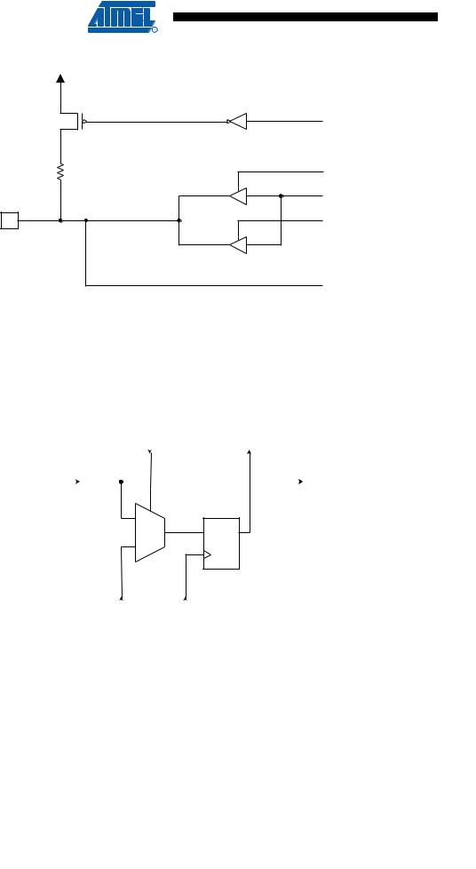
Figure 24-5. Additional Scan Signal for the Two-wire Interface
|
PUExn |
|
OCxn |
|
ODxn |
Pxn |
TWIEN |
|
SRC |
|
Slew-rate Limited |
|
IDxn |
24.5.3Scanning the RESET Pin
The RESET pin accepts 5V active low logic for standard reset operation, and 12V active high logic for High Voltage Parallel Programming. An observe-only cell as shown in Figure 24-6 is inserted both for the 5V reset signal; RSTT, and the 12V reset signal; RSTHV.
Figure 24-6. Observe-only Cell
|
|
To |
|
|
|
Next |
|
|
ShiftDR |
Cell |
|
From System Pin |
|
|
To System Logic |
|
|
||
FF1
0
D Q
1
From ClockDR
Previous
Cell
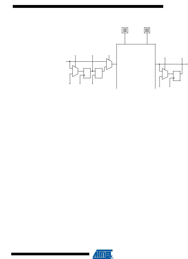
24.5.4Scanning the Clock Pins
The AVR devices have many clock options selectable by fuses. These are: Internal RC Oscillator, External RC, External Clock, (High Frequency) Crystal Oscillator, Low Frequency Crystal Oscillator, and Ceramic Resonator.
Figure 24-7 shows how each Oscillator with external connection is supported in the scan chain. The Enable signal is supported with a general boundary-scan cell, while the Oscillator/Clock output is attached to an observe-only cell. In addition to the main clock, the Timer Oscillator is scanned in the same way. The output from the internal RC Oscillator is not scanned, as this Oscillator does not have external connections.
238 ATmega16A 
8154A–AVR–06/08
ATmega16A
Figure 24-7. Boundary-scan Cells for Oscillators and Clock Options
XTAL1/TOSC1 XTAL2/TOSC2
|
|
To |
|
|
|
|
|
|
|
Next |
|
|
Oscillator |
|
To |
Logic |
ShiftDR |
Cell |
|
EXTEST |
|
Next |
|
|
|
|
|
ShiftDR |
|
Cell |
|
Digital |
|
|
|
|
|
||
|
|
|
0 |
OUTPUT |
|
|
|
From |
0 |
|
|
ENABLE |
FF1 |
||
|
|
1 |
|
||||
|
|
|
|
|
|
|
|
|
D |
Q |
D |
Q |
0 |
|
|
|
1 |
|
|
|
D |
Q |
|
|
|
G |
|
|
|||
|
|
|
|
1 |
|||
|
|
|
|
|
|
||
|
|
|
|
|
|
|
|
From |
ClockDR |
UpdateDR |
|
||
Previous |
|
|
|
From |
ClockDR |
Cell |
|
|
|
Previous |
|
|
|
|
|
Cell |
|
To System Logic
Table 24-4 summaries the scan registers for the external clock pin XTAL1, Oscillators with XTAL1/XTAL2 connections as well as 32 kHz Timer Oscillator.
Table 24-4. |
Scan Signals for the Oscillators(1)(2)(3) |
|
||
|
|
|
|
Scanned Clock Line |
Enable Signal |
|
Scanned Clock Line |
Clock Option |
when not Used |
|
|
|
|
|
EXTCLKEN |
|
EXTCLK (XTAL1) |
External Clock |
0 |
|
|
|
|
|
OSCON |
|
OSCCK |
External Crystal |
0 |
|
|
|
External Ceramic Resonator |
|
|
|
|
|
|
RCOSCEN |
|
RCCK |
External RC |
1 |
|
|
|
|
|
OSC32EN |
|
OSC32CK |
Low Freq. External Crystal |
0 |
|
|
|
|
|
TOSKON |
|
TOSCK |
32 kHz Timer Oscillator |
0 |
|
|
|
|
|
Notes: 1. Do not enable more than one clock source as main clock at a time.
2.Scanning an Oscillator output gives unpredictable results as there is a frequency drift between the Internal Oscillator and the JTAG TCK clock. If possible, scanning an external clock is preferred.
3.The clock configuration is programmed by fuses. As a fuse is not changed run-time, the clock configuration is considered fixed for a given application. The user is advised to scan the same clock option as to be used in the final system. The enable signals are supported in the scan chain because the system logic can disable clock options in sleep modes, thereby disconnecting the Oscillator pins from the scan path if not provided. The INTCAP Fuses are not supported in the scan-chain, so the boundary scan chain can not make a XTAL Oscillator requiring internal capacitors to run unless the fuse is correctly programmed.
24.5.5Scanning the Analog Comparator
The relevant Comparator signals regarding Boundary-scan are shown in Figure 24-8. The Boundary-scan cell from Figure 24-9 is attached to each of these signals. The signals are described in Table 24-5.
The Comparator need not be used for pure connectivity testing, since all analog inputs are shared with a digital port pin as well.
239
8154A–AVR–06/08
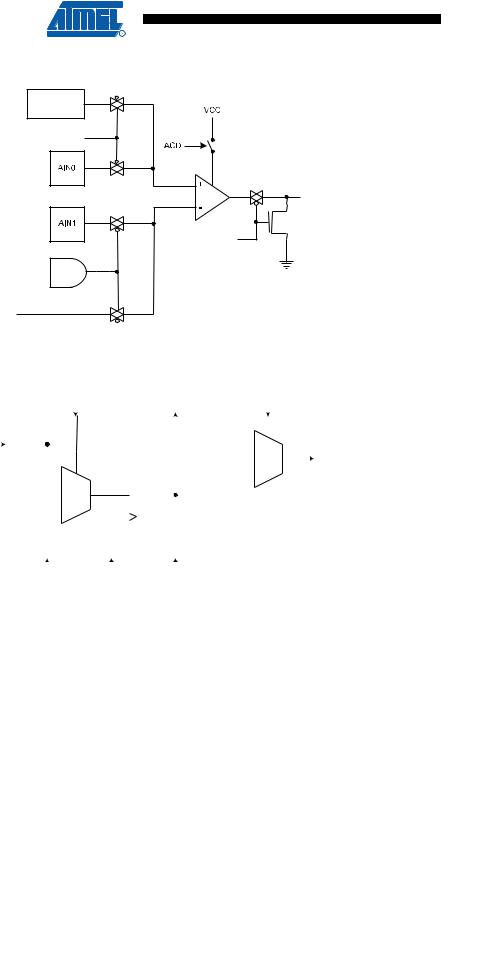
Figure 24-8. Analog Comparator
BANDGAP
REFERENCE
ACBG
ACO
AC_IDLE
ACME
ADCEN 
ADC MULTIPLEXER
OUTPUT
Figure 24-9. General Boundary-scan Cell used for Signals for Comparator and ADC
|
|
|
|
|
|
|
To |
|
|
|
|
|
|
|
|
|
|
|
|
|
|
|
Next |
|
|
|
|
|
|
|
|
||
|
|
ShiftDR |
Cell |
|
|
EXTEST |
|
|||||||||
From Digital Logic/ |
|
|
|
|
|
|
|
|
|
|
|
|
|
|||
|
|
|
|
|
|
|
|
|
|
|
|
|
|
|
|
|
|
|
|
|
|
|
|
|
|
|
|
|
|
|
|
|
|
|
|
|
|
|
|
0 |
|
|
|
|||||||
From Analog Ciruitry |
|
|
|
|
|
|
|
|
|
To Analog Circuitry/ |
||||||
|
|
|
|
|
|
|
|
|
|
|
|
|
|
|||
|
|
|
0 |
|
|
|
|
|
|
|
1 |
|
|
To Digital Logic |
||
|
|
|
|
|
|
|
|
|
|
|
||||||
|
|
|
D |
Q |
|
|
D Q |
|
|
|
|
|
|
|
||
|
|
|
1 |
|
|
|
|
|
|
|
|
|
|
|||
|
|
|
|
|
|
|
|
|
|
|
|
|
||||
|
|
|
|
|
|
|
|
G |
|
|
|
|
|
|
|
|
|
|
|
|
|
|
|
|
|
|
|
|
|
|
|
|
|
|
|
|
|
|
|
|
|
|
|
|
|
|
|
|
|
|
|
|
|
|
|
|
|
|
|
|
|
|
|
|
|
|
|
|
|
|
|
|
|
|
|
|
|
|
|
|
|
|
|
|
From ClockDR UpdateDR
Previous
Cell
240 ATmega16A 
8154A–AVR–06/08
 ATmega16A
Table 24-5. |
Boundary-scan Signals for the Analog Comparator |
|
||
Signal |
Direction as Seen from |
|
Recommended Input |
Output Values when |
Name |
the Comparator |
Description |
when Not in Use |
Recommended Inputs are Used |
|
|
|
|
|
AC_IDLE |
Input |
Turns off Analog |
1 |
Depends upon µC code being |
|
|
comparator when true |
|
executed |
|
|
|
|
|
ACO |
Output |
Analog Comparator |
Will become input to µC |
0 |
|
|
Output |
code being executed |
|
|
|
|
|
|
ACME |
Input |
Uses output signal from |
0 |
Depends upon µC code being |
|
|
ADC mux when true |
|
executed |
|
|
|
|
|
ACBG |
Input |
Bandgap Reference |
0 |
Depends upon µC code being |
|
|
enable |
|
executed |
|
|
|
|
|
24.5.6Scanning the ADC
Figure 24-10 shows a block diagram of the ADC with all relevant control and observe signals. The Boundary-scan cell from Figure 24-9 is attached to each of these signals. The ADC need not be used for pure connectivity testing, since all analog inputs are shared with a digital port pin as well.
Figure 24-10. Analog to Digital Converter
VCCREN 
AREF 
IREFEN
|
To Comparator |
2.56V |
|
|
|
ref |
|
|
|
MUXEN_7 |
|
PASSEN |
|
|
|
|
|
|
|
ADC_7 |
|
|
|
|
MUXEN_6 |
|
|
|
|
ADC_6 |
|
|
|
|
MUXEN_5 |
|
|
|
|
ADC_5 |
|
|
|
|
MUXEN_4 |
SCTEST |
ADCBGEN |
|
|
ADC_4 |
|
|
|
|
|
|
|
|
|
EXTCH |
|
1.22V |
PRECH |
|
MUXEN_3 |
|
ref |
AREF |
|
|
|
|
||
|
|
AREF |
|
|
|
|
|
|
|
ADC_3 |
|
|
|
DACOUT |
MUXEN_2 |
|
|
|
|
|
|
|
|
|
ADC_2 |
|
|
DAC_9..0 |
|
MUXEN_1 |
|
|
10-bit DAC |
+ |
|
|
|
COMP |
|
ADC_1 |
G10 |
G20 |
ADCEN |
- |
MUXEN_0 |
|
|
|
|
|
ACTEN |
|
|
|
ADC_0 |
+ |
|
|
|
+ |
|
|
||
|
|
|
||
NEGSEL_2 |
10x |
20x |
HOLD |
|
ADC_2 |
- |
- |
|
NEGSEL_1 |
GNDEN |
|
ADC_1 |
||
|
NEGSEL_0
ST
ACLK
ADC_0
AMPEN 
 COMP
COMP
241
8154A–AVR–06/08

The signals are described briefly in Table 24-6.
Table 24-6. |
Boundary-scan Signals for the ADC |
|
|
|
|
|
|
Recommended |
Output Values when Recommended |
Signal |
Direction as Seen |
|
Input when Not |
Inputs are used, and CPU is not |
Name |
from the ADC |
Description |
in Use |
Using the ADC |
|
|
|
|
|
COMP |
Output |
Comparator Output |
0 |
0 |
|
|
|
|
|
ACLK |
Input |
Clock signal to gain stages |
0 |
0 |
|
|
implemented as Switch-cap filters |
|
|
|
|
|
|
|
ACTEN |
Input |
Enable path from gain stages to |
0 |
0 |
|
|
the comparator |
|
|
|
|
|
|
|
ADCBGEN |
Input |
Enable Band-gap reference as |
0 |
0 |
|
|
negative input to comparator |
|
|
|
|
|
|
|
ADCEN |
Input |
Power-on signal to the ADC |
0 |
0 |
|
|
|
|
|
AMPEN |
Input |
Power-on signal to the gain stages |
0 |
0 |
|
|
|
|
|
DAC_9 |
Input |
Bit 9 of digital value to DAC |
1 |
1 |
|
|
|
|
|
DAC_8 |
Input |
Bit 8 of digital value to DAC |
0 |
0 |
|
|
|
|
|
DAC_7 |
Input |
Bit 7 of digital value to DAC |
0 |
0 |
|
|
|
|
|
DAC_6 |
Input |
Bit 6 of digital value to DAC |
0 |
0 |
|
|
|
|
|
DAC_5 |
Input |
Bit 5 of digital value to DAC |
0 |
0 |
|
|
|
|
|
DAC_4 |
Input |
Bit 4 of digital value to DAC |
0 |
0 |
|
|
|
|
|
DAC_3 |
Input |
Bit 3 of digital value to DAC |
0 |
0 |
|
|
|
|
|
DAC_2 |
Input |
Bit 2 of digital value to DAC |
0 |
0 |
|
|
|
|
|
DAC_1 |
Input |
Bit 1 of digital value to DAC |
0 |
0 |
|
|
|
|
|
DAC_0 |
Input |
Bit 0 of digital value to DAC |
0 |
0 |
|
|
|
|
|
EXTCH |
Input |
Connect ADC channels 0 - 3 to by- |
1 |
1 |
|
|
pass path around gain stages |
|
|
|
|
|
|
|
G10 |
Input |
Enable 10x gain |
0 |
0 |
|
|
|
|
|
G20 |
Input |
Enable 20x gain |
0 |
0 |
|
|
|
|
|
GNDEN |
Input |
Ground the negative input to |
0 |
0 |
|
|
comparator when true |
|
|
|
|
|
|
|
HOLD |
Input |
Sample&Hold signal. Sample |
1 |
1 |
|
|
analog signal when low. Hold |
|
|
|
|
signal when high. If gain stages |
|
|
|
|
are used, this signal must go |
|
|
|
|
active when ACLK is high. |
|
|
|
|
|
|
|
IREFEN |
Input |
Enables Band-gap reference as |
0 |
0 |
|
|
AREF signal to DAC |
|
|
|
|
|
|
|
MUXEN_7 |
Input |
Input Mux bit 7 |
0 |
0 |
|
|
|
|
|
MUXEN_6 |
Input |
Input Mux bit 6 |
0 |
0 |
|
|
|
|
|
MUXEN_5 |
Input |
Input Mux bit 5 |
0 |
0 |
|
|
|
|
|
MUXEN_4 |
Input |
Input Mux bit 4 |
0 |
0 |
|
|
|
|
|
242 ATmega16A 
8154A–AVR–06/08

 ATmega16A
Table 24-6. |
Boundary-scan Signals for the ADC (Continued) |
|
|
|
|
|
|
Recommended |
Output Values when Recommended |
Signal |
Direction as Seen |
|
Input when Not |
Inputs are used, and CPU is not |
Name |
from the ADC |
Description |
in Use |
Using the ADC |
|
|
|
|
|
MUXEN_3 |
Input |
Input Mux bit 3 |
0 |
0 |
|
|
|
|
|
MUXEN_2 |
Input |
Input Mux bit 2 |
0 |
0 |
|
|
|
|
|
MUXEN_1 |
Input |
Input Mux bit 1 |
0 |
0 |
|
|
|
|
|
MUXEN_0 |
Input |
Input Mux bit 0 |
1 |
1 |
|
|
|
|
|
NEGSEL_2 |
Input |
Input Mux for negative input for |
0 |
0 |
|
|
differential signal, bit 2 |
|
|
|
|
|
|
|
NEGSEL_1 |
Input |
Input Mux for negative input for |
0 |
0 |
|
|
differential signal, bit 1 |
|
|
|
|
|
|
|
NEGSEL_0 |
Input |
Input Mux for negative input for |
0 |
0 |
|
|
differential signal, bit 0 |
|
|
|
|
|
|
|
PASSEN |
Input |
Enable pass-gate of gain stages. |
1 |
1 |
|
|
|
|
|
PRECH |
Input |
Precharge output latch of |
1 |
1 |
|
|
comparator. (Active low) |
|
|
|
|
|
|
|
SCTEST |
Input |
Switch-cap TEST enable. Output |
0 |
0 |
|
|
from x10 gain stage send out to |
|
|
|
|
Port Pin having ADC_4 |
|
|
|
|
|
|
|
ST |
Input |
Output of gain stages will settle |
0 |
0 |
|
|
faster if this signal is high first two |
|
|
|
|
ACLK periods after AMPEN goes |
|
|
|
|
high. |
|
|
|
|
|
|
|
VCCREN |
Input |
Selects Vcc as the ACC reference |
0 |
0 |
|
|
voltage. |
|
|
|
|
|
|
|
Note: Incorrect setting of the switches in Figure 24-10 will make signal contention and may damage the part. There are several input choices to the S&H circuitry on the negative input of the output comparator in Figure 24-10. Make sure only one path is selected from either one ADC pin, Bandgap reference source, or Ground.
If the ADC is not to be used during scan, the recommended input values from Table 24-6 should be used. The user is recommended not to use the Differential Gain stages during scan. Switchcap based gain stages require fast operation and accurate timing which is difficult to obtain when used in a scan chain. Details concerning operations of the differential gain stage is therefore not provided.
The AVR ADC is based on the analog circuitry shown in Figure 24-10 with a successive approximation algorithm implemented in the digital logic. When used in Boundary-scan, the problem is usually to ensure that an applied analog voltage is measured within some limits. This can easily be done without running a successive approximation algorithm: apply the lower limit on the digital DAC[9:0] lines, make sure the output from the comparator is low, then apply the upper limit on the digital DAC[9:0] lines, and verify the output from the comparator to be high.
The ADC need not be used for pure connectivity testing, since all analog inputs are shared with a digital port pin as well.
When using the ADC, remember the following:
•The Port Pin for the ADC channel in use must be configured to be an input with pull-up disabled to avoid signal contention.
243
8154A–AVR–06/08

•In Normal mode, a dummy conversion (consisting of 10 comparisons) is performed when enabling the ADC. The user is advised to wait at least 200 ns after enabling the ADC before controlling/observing any ADC signal, or perform a dummy conversion before using the first result.
•The DAC values must be stable at the midpoint value 0x200 when having the HOLD signal low (Sample mode).
As an example, consider the task of verifying a 1.5V ± 5% input signal at ADC channel 3 when the power supply is 5.0V and AREF is externally connected to VCC.
The lower limit is: |
|
1024 1,5V 0,95 ⁄ 5V |
|
|
= 291 = 0x123 |
|
|
|
|
||||
The upper limit is: |
|
|
1024 1,5V 1,05 ⁄ 5V |
|
= 323 = 0x143 |
|
|
|
|
||||
The recommended values from Table 24-6 are used unless other values are given in the algorithm in Table 24-7. Only the DAC and Port Pin values of the Scan-chain are shown. The column “Actions” describes what JTAG instruction to be used before filling the Boundary-scan Register with the succeeding columns. The verification should be done on the data scanned out when scanning in the data on the same row in the table.
Table 24-7. Algorithm for Using the ADC
|
|
|
|
|
|
|
|
|
PA3. |
|
|
|
|
|
|
|
PA3. |
PA3. |
Pullup_ |
Step |
Actions |
ADCEN |
DAC |
MUXEN |
HOLD |
PRECH |
Data |
Control |
Enable |
|
|
|
|
|
|
|
|
|
|
1 |
SAMPLE_ |
1 |
0x200 |
0x08 |
1 |
1 |
0 |
0 |
0 |
|
PRELOAD |
|
|
|
|
|
|
|
|
|
|
|
|
|
|
|
|
|
|
2 |
EXTEST |
1 |
0x200 |
0x08 |
0 |
1 |
0 |
0 |
0 |
|
|
|
|
|
|
|
|
|
|
3 |
|
1 |
0x200 |
0x08 |
1 |
1 |
0 |
0 |
0 |
|
|
|
|
|
|
|
|
|
|
4 |
|
1 |
0x123 |
0x08 |
1 |
1 |
0 |
0 |
0 |
|
|
|
|
|
|
|
|
|
|
5 |
|
1 |
0x123 |
0x08 |
1 |
0 |
0 |
0 |
0 |
|
|
|
|
|
|
|
|
|
|
6 |
Verify the |
1 |
0x200 |
0x08 |
1 |
1 |
0 |
0 |
0 |
|
COMP bit |
|
|
|
|
|
|
|
|
|
scanned |
|
|
|
|
|
|
|
|
|
out to be 0 |
|
|
|
|
|
|
|
|
|
|
|
|
|
|
|
|
|
|
7 |
|
1 |
0x200 |
0x08 |
0 |
1 |
0 |
0 |
0 |
|
|
|
|
|
|
|
|
|
|
8 |
|
1 |
0x200 |
0x08 |
1 |
1 |
0 |
0 |
0 |
|
|
|
|
|
|
|
|
|
|
9 |
|
1 |
0x143 |
0x08 |
1 |
1 |
0 |
0 |
0 |
|
|
|
|
|
|
|
|
|
|
10 |
|
1 |
0x143 |
0x08 |
1 |
0 |
0 |
0 |
0 |
|
|
|
|
|
|
|
|
|
|
11 |
Verify the |
1 |
0x200 |
0x08 |
1 |
1 |
0 |
0 |
0 |
|
COMP bit |
|
|
|
|
|
|
|
|
|
scanned |
|
|
|
|
|
|
|
|
|
out to be 1 |
|
|
|
|
|
|
|
|
|
|
|
|
|
|
|
|
|
|
Using this algorithm, the timing constraint on the HOLD signal constrains the TCK clock frequency. As the algorithm keeps HOLD high for five steps, the TCK clock frequency has to be at least five times the number of scan bits divided by the maximum hold time, thold,max.
244 ATmega16A 
8154A–AVR–06/08

 ATmega16A
24.6Boundary-scan Order
Table 24-8 shows the scan order between TDI and TDO when the Boundary-scan chain is selected as data path. Bit 0 is the LSB; the first bit scanned in, and the first bit scanned out. The scan order follows the pin-out order as far as possible. Therefore, the bits of Port A is scanned in the opposite bit order of the other ports. Exceptions from the rules are the Scan chains for the analog circuits, which constitute the most significant bits of the scan chain regardless of which physical pin they are connected to. In Figure 24-3, PXn. Data corresponds to FF0, PXn. Control corresponds to FF1, and PXn. Pullup_enable corresponds to FF2. Bit 2, 3, 4, and 5 of Port C is not in the scan chain, since these pins constitute the TAP pins when the JTAG is enabled.
Table 24-8. ATmega16A Boundary-scan Order
Bit Number |
Signal Name |
Module |
|
|
|
140 |
AC_IDLE |
Comparator |
|
|
|
139 |
ACO |
|
|
|
|
138 |
ACME |
|
|
|
|
137 |
ACBG |
|
|
|
|
136 |
COMP |
ADC |
|
|
|
135 |
PRIVATE_SIGNAL1(1) |
|
134 |
ACLK |
|
|
|
|
133 |
ACTEN |
|
|
|
|
132 |
PRIVATE_SIGNAL2(2) |
|
131 |
ADCBGEN |
|
|
|
|
130 |
ADCEN |
|
|
|
|
129 |
AMPEN |
|
|
|
|
128 |
DAC_9 |
|
|
|
|
127 |
DAC_8 |
|
|
|
|
126 |
DAC_7 |
|
|
|
|
125 |
DAC_6 |
|
|
|
|
124 |
DAC_5 |
|
|
|
|
123 |
DAC_4 |
|
|
|
|
122 |
DAC_3 |
|
|
|
|
121 |
DAC_2 |
|
|
|
|
120 |
DAC_1 |
|
|
|
|
119 |
DAC_0 |
|
|
|
|
118 |
EXTCH |
|
|
|
|
117 |
G10 |
|
|
|
|
116 |
G20 |
|
|
|
|
115 |
GNDEN |
|
|
|
|
114 |
HOLD |
|
|
|
|
113 |
IREFEN |
|
|
|
|
112 |
MUXEN_7 |
|
|
|
|
245
8154A–AVR–06/08

|
|
Table 24-8. |
|
|
|
|
|
|
|
|
|
|
|
|
|
|
|
|
|
|
|
|
|
ATmega16A Boundary-scan Order (Continued) |
||||||||
|
|
|
|
|
|
|
|
|
|
|
|
|
Bit Number |
|
Signal Name |
Module |
|
||||
|
|
|
|
|
|
|
|
|
|
|
|
|
111 |
|
MUXEN_6 |
|
|
|
|||
|
|
|
|
|
|
|
|
|
|
|
|
|
110 |
|
MUXEN_5 |
|
|
|
|||
|
|
|
|
|
|
|
|
|
|
|
|
|
109 |
|
MUXEN_4 |
|
|
|
|||
|
|
|
|
|
|
|
|
|
|
|
|
|
108 |
|
MUXEN_3 |
|
|
|
|||
|
|
|
|
|
|
|
|
|
|
|
|
|
107 |
|
MUXEN_2 |
|
|
|
|||
|
|
|
|
|
|
|
|
|
|
|
|
|
106 |
|
MUXEN_1 |
|
|
|
|||
|
|
|
|
|
|
|
|
|
|
|
|
|
105 |
|
MUXEN_0 |
|
|
|
|||
|
|
|
|
|
|
|
|
|
|
|
|
|
104 |
|
NEGSEL_2 |
|
|
|
|||
|
|
|
|
|
|
|
|
|
|
|
|
|
103 |
|
NEGSEL_1 |
|
|
|
|||
|
|
|
|
|
|
|
|
|
|
|
|
|
102 |
|
NEGSEL_0 |
|
|
|
|||
|
|
|
|
|
|
|
|
|
|
|
|
|
101 |
|
PASSEN |
|
|
|
|||
|
|
|
|
|
|
|
|
|
|
|
|
|
100 |
|
PRECH |
|
|
|
|||
|
|
|
|
|
|
|
|
|
|
|
|
|
99 |
|
SCTEST |
|
|
|
|||
|
|
|
|
|
|
|
|
|
|
|
|
|
98 |
|
ST |
|
|
|
|||
|
|
|
|
|
|
|
|
|
|
|
|
|
97 |
|
VCCREN |
|
|
|
|||
|
|
|
|
|
|
|
|
|
|
|
|
|
96 |
|
PB0.Data |
Port B |
|
||||
|
|
|
|
|
|
|
|
|
|
|
|
|
95 |
|
PB0.Control |
|
|
|
|||
|
|
|
|
|
|
|
|
|
|
|
|
|
94 |
|
PB0.Pullup_Enable |
|
|
|
|||
|
|
|
|
|
|
|
|
|
|
|
|
|
93 |
|
PB1.Data |
|
|
|
|||
|
|
|
|
|
|
|
|
|
|
|
|
|
92 |
|
PB1.Control |
|
|
|
|||
|
|
|
|
|
|
|
|
|
|
|
|
|
91 |
|
PB1.Pullup_Enable |
|
|
|
|||
|
|
|
|
|
|
|
|
|
|
|
|
|
90 |
|
PB2.Data |
|
|
|
|||
|
|
|
|
|
|
|
|
|
|
|
|
|
89 |
|
PB2.Control |
|
|
|
|||
|
|
|
|
|
|
|
|
|
|
|
|
|
88 |
|
PB2.Pullup_Enable |
|
|
|
|||
|
|
|
|
|
|
|
|
|
|
|
|
|
87 |
|
PB3.Data |
|
|
|
|||
|
|
|
|
|
|
|
|
|
|
|
|
|
86 |
|
PB3.Control |
|
|
|
|||
|
|
|
|
|
|
|
|
|
|
|
|
|
85 |
|
PB3.Pullup_Enable |
|
|
|
|||
|
|
|
|
|
|
|
|
|
|
|
|
|
84 |
|
PB4.Data |
|
|
|
|||
|
|
|
|
|
|
|
|
|
|
|
|
|
83 |
|
PB4.Control |
|
|
|
|||
|
|
|
|
|
|
|
|
|
|
|
|
|
82 |
|
PB4.Pullup_Enable |
|
|
|
|||
|
|
|
|
|
|
|
|
|
|
|
|
|
81 |
|
PB5.Data |
|
|
|
|||
|
|
|
|
|
|
|
|
|
|
|
|
|
80 |
|
PB5.Control |
|
|
|
|||
|
|
|
|
|
|
|
|
|
|
|
|
|
79 |
|
PB5.Pullup_Enable |
|
|
|
|||
|
|
|
|
|
|
|
|
|
|
|
|
|
78 |
|
PB6.Data |
|
|
|
|||
|
|
|
|
|
|
|
|
|
|
|
|
|
77 |
|
PB6.Control |
|
|
|
|||
|
|
|
|
|
|
|
|
|
|
|
|
|
76 |
|
PB6.Pullup_Enable |
|
|
|
|||
|
|
|
|
|
|
|
|
|
|
|
246 |
ATmega16A |
|
|
|
|
|
|
|
|
|
8154A–AVR–06/08

 ATmega16A
Table 24-8. |
ATmega16A Boundary-scan Order (Continued) |
||
Bit Number |
|
Signal Name |
Module |
|
|
|
|
75 |
|
PB7.Data |
|
|
|
|
|
74 |
|
PB7.Control |
|
|
|
|
|
73 |
|
PB7.Pullup_Enable |
|
|
|
|
|
72 |
|
RSTT |
Reset Logic |
|
|
|
(Observe-Only) |
71 |
|
RSTHV |
|
|
|
||
|
|
|
|
70 |
|
EXTCLKEN |
Enable signals for main clock/Oscillators |
|
|
|
|
69 |
|
OSCON |
|
|
|
|
|
68 |
|
RCOSCEN |
|
|
|
|
|
67 |
|
OSC32EN |
|
|
|
|
|
66 |
|
EXTCLK (XTAL1) |
Clock input and Oscillators for the main clock |
|
|
|
(Observe-Only) |
65 |
|
OSCCK |
|
|
|
||
|
|
|
|
64 |
|
RCCK |
|
|
|
|
|
63 |
|
OSC32CK |
|
|
|
|
|
62 |
|
TWIEN |
TWI |
|
|
|
|
61 |
|
PD0.Data |
Port D |
|
|
|
|
60 |
|
PD0.Control |
|
|
|
|
|
59 |
|
PD0.Pullup_Enable |
|
|
|
|
|
58 |
|
PD1.Data |
|
|
|
|
|
57 |
|
PD1.Control |
|
|
|
|
|
56 |
|
PD1.Pullup_Enable |
|
|
|
|
|
55 |
|
PD2.Data |
|
|
|
|
|
54 |
|
PD2.Control |
|
|
|
|
|
53 |
|
PD2.Pullup_Enable |
|
|
|
|
|
52 |
|
PD3.Data |
|
|
|
|
|
51 |
|
PD3.Control |
|
|
|
|
|
50 |
|
PD3.Pullup_Enable |
|
|
|
|
|
49 |
|
PD4.Data |
|
|
|
|
|
48 |
|
PD4.Control |
|
|
|
|
|
47 |
|
PD4.Pullup_Enable |
|
|
|
|
|
46 |
|
PD5.Data |
|
|
|
|
|
45 |
|
PD5.Control |
|
|
|
|
|
44 |
|
PD5.Pullup_Enable |
|
|
|
|
|
43 |
|
PD6.Data |
|
|
|
|
|
42 |
|
PD6.Control |
|
|
|
|
|
41 |
|
PD6.Pullup_Enable |
|
|
|
|
|
40 |
|
PD7.Data |
|
|
|
|
|
247
8154A–AVR–06/08

Table 24-8. |
|
|
|
|
|
|
|
|
|
|
|
|
|
|
|
|
|
ATmega16A Boundary-scan Order (Continued) |
||||||||
|
|
|
|
|
|
|
|
|
Bit Number |
|
Signal Name |
Module |
|
||||
|
|
|
|
|
|
|
|
|
39 |
|
PD7.Control |
|
|
|
|||
|
|
|
|
|
|
|
|
|
38 |
|
PD7.Pullup_Enable |
|
|
|
|||
|
|
|
|
|
|
|
|
|
37 |
|
PC0.Data |
Port C |
|
||||
|
|
|
|
|
|
|
|
|
36 |
|
PC0.Control |
|
|
|
|||
|
|
|
|
|
|
|
|
|
35 |
|
PC0.Pullup_Enable |
|
|
|
|||
|
|
|
|
|
|
|
|
|
34 |
|
PC1.Data |
|
|
|
|||
|
|
|
|
|
|
|
|
|
33 |
|
PC1.Control |
|
|
|
|||
|
|
|
|
|
|
|
|
|
32 |
|
PC1.Pullup_Enable |
|
|
|
|||
|
|
|
|
|
|
|
|
|
31 |
|
PC6.Data |
|
|
|
|||
|
|
|
|
|
|
|
|
|
30 |
|
PC6.Control |
|
|
|
|||
|
|
|
|
|
|
|
|
|
29 |
|
PC6.Pullup_Enable |
|
|
|
|||
|
|
|
|
|
|
|
|
|
28 |
|
PC7.Data |
|
|
|
|||
|
|
|
|
|
|
|
|
|
27 |
|
PC7.Control |
|
|
|
|||
|
|
|
|
|
|
|
|
|
26 |
|
PC7.Pullup_Enable |
|
|
|
|||
|
|
|
|
|
|
|
|
|
25 |
|
TOSC |
32 kHz Timer Oscillator |
|
||||
|
|
|
|
|
|
|
|
|
24 |
|
TOSCON |
|
|
|
|||
|
|
|
|
|
|
|
|
|
23 |
|
PA7.Data |
Port A |
|
||||
|
|
|
|
|
|
|
|
|
22 |
|
PA7.Control |
|
|
|
|||
|
|
|
|
|
|
|
|
|
21 |
|
PA7.Pullup_Enable |
|
|
|
|||
|
|
|
|
|
|
|
|
|
20 |
|
PA6.Data |
|
|
|
|||
|
|
|
|
|
|
|
|
|
19 |
|
PA6.Control |
|
|
|
|||
|
|
|
|
|
|
|
|
|
18 |
|
PA6.Pullup_Enable |
|
|
|
|||
|
|
|
|
|
|
|
|
|
17 |
|
PA5.Data |
|
|
|
|||
|
|
|
|
|
|
|
|
|
16 |
|
PA5.Control |
|
|
|
|||
|
|
|
|
|
|
|
|
|
15 |
|
PA5.Pullup_Enable |
|
|
|
|||
|
|
|
|
|
|
|
|
|
14 |
|
PA4.Data |
|
|
|
|||
|
|
|
|
|
|
|
|
|
13 |
|
PA4.Control |
|
|
|
|||
|
|
|
|
|
|
|
|
|
12 |
|
PA4.Pullup_Enable |
|
|
|
|||
|
|
|
|
|
|
|
|
|
11 |
|
PA3.Data |
|
|
|
|||
|
|
|
|
|
|
|
|
|
10 |
|
PA3.Control |
|
|
|
|||
|
|
|
|
|
|
|
|
|
9 |
|
PA3.Pullup_Enable |
|
|
|
|||
|
|
|
|
|
|
|
|
|
8 |
|
PA2.Data |
|
|
|
|||
|
|
|
|
|
|
|
|
|
7 |
|
PA2.Control |
|
|
|
|||
|
|
|
|
|
|
|
|
|
6 |
|
PA2.Pullup_Enable |
|
|
|
|||
|
|
|
|
|
|
|
|
|
5 |
|
PA1.Data |
|
|
|
|||
|
|
|
|
|
|
|
|
|
248 ATmega16A 
8154A–AVR–06/08