

- •Features
- •1. Pin Configurations
- •2. Overview
- •2.1 Block Diagram
- •2.2 Pin Descriptions
- •2.2.3 Port A (PA7:PA0)
- •2.2.4 Port B (PB7:PB0)
- •2.2.5 Port C (PC7:PC0)
- •2.2.6 Port D (PD7:PD0)
- •2.2.7 RESET
- •2.2.8 XTAL1
- •2.2.9 XTAL2
- •2.2.10 AVCC
- •2.2.11 AREF
- •3. Resources
- •4. Data Retention
- •5. About Code Examples
- •6.1 Overview
- •6.3 Status Register
- •6.3.1 SREG – AVR Status Register
- •6.4 General Purpose Register File
- •6.5 Stack Pointer
- •6.5.1 SPH and SPL – Stack Pointer High and Low Register
- •6.6 Instruction Execution Timing
- •6.7 Reset and Interrupt Handling
- •6.7.1 Interrupt Response Time
- •7. AVR Memories
- •7.1 Overview
- •7.3 SRAM Data Memory
- •7.3.1 Data Memory Access Times
- •7.4 EEPROM Data Memory
- •7.4.1 EEPROM Read/Write Access
- •7.4.3 Preventing EEPROM Corruption
- •7.5 I/O Memory
- •7.6 Register Description
- •7.6.1 EEARH and EEARL – The EEPROM Address Register
- •7.6.2 EEDR – The EEPROM Data Register
- •7.6.3 EECR – The EEPROM Control Register
- •8. System Clock and Clock Options
- •8.1 Clock Systems and their Distribution
- •8.2 Clock Sources
- •8.3 Default Clock Source
- •8.4 Crystal Oscillator
- •8.6 External RC Oscillator
- •8.7 Calibrated Internal RC Oscillator
- •8.8 External Clock
- •8.9 Timer/Counter Oscillator
- •8.10 Register Description
- •8.10.1 OSCCAL – Oscillator Calibration Register
- •9. Power Management and Sleep Modes
- •9.1 Overview
- •9.2 Sleep Modes
- •9.3 Idle Mode
- •9.4 ADC Noise Reduction Mode
- •9.7 Standby Mode
- •9.8 Extended Standby Mode
- •9.9 Minimizing Power Consumption
- •9.9.1 Analog to Digital Converter
- •9.9.2 Analog Comparator
- •9.9.4 Internal Voltage Reference
- •9.9.5 Watchdog Timer
- •9.9.6 Port Pins
- •9.10 Register Description
- •9.10.1 MCUCR – MCU Control Register
- •10. System Control and Reset
- •10.1 Resetting the AVR
- •10.1.1 Reset Sources
- •10.1.3 External Reset
- •10.1.5 Watchdog Reset
- •10.2 Internal Voltage Reference
- •10.3 Watchdog Timer
- •10.4 Register Description
- •10.4.1 MCUCSR – MCU Control and Status Register
- •10.4.2 WDTCR – Watchdog Timer Control Register
- •11. Interrupts
- •11.1 Overview
- •11.2 Interrupt Vectors
- •11.2.1 Moving Interrupts Between Application and Boot Space
- •11.2.2 GICR – General Interrupt Control Register
- •12. I/O Ports
- •12.1 Overview
- •12.2 Ports as General Digital I/O
- •12.2.1 Configuring the Pin
- •12.2.2 Reading the Pin Value
- •12.2.3 Digital Input Enable and Sleep Modes
- •12.2.4 Unconnected pins
- •12.3 Alternate Port Functions
- •12.3.1 Alternate Functions of Port A
- •12.3.2 Alternate Functions of Port B
- •12.3.3 Alternate Functions of Port C
- •12.3.4 Alternate Functions of Port D
- •12.4 Register Description
- •12.4.1 SFIOR – Special Function I/O Register
- •12.4.2 PORTA – Port A Data Register
- •12.4.3 DDRA – Port A Data Direction Register
- •12.4.4 PINA – Port A Input Pins Address
- •12.4.5 PORTB – Port B Data Register
- •12.4.6 DDRB – Port B Data Direction Register
- •12.4.7 PINB – Port B Input Pins Address
- •12.4.8 PORTC – Port C Data Register
- •12.4.9 DDRC – Port C Data Direction Register
- •12.4.10 PINC – Port C Input Pins Address
- •12.4.11 PORTD – Port D Data Register
- •12.4.12 DDRD – Port D Data Direction Register
- •12.4.13 PIND – Port D Input Pins Address
- •13. External Interrupts
- •13.1 Register Description
- •13.1.1 MCUCR – MCU Control Register
- •13.1.2 MCUCSR – MCU Control and Status Register
- •13.1.3 GICR – General Interrupt Control Register
- •13.1.4 GIFR – General Interrupt Flag Register
- •14. 8-bit Timer/Counter0 with PWM
- •14.1 Features
- •14.2 Overview
- •14.2.1 Registers
- •14.2.2 Definitions
- •14.3 Timer/Counter Clock Sources
- •14.4 Counter Unit
- •14.5 Output Compare Unit
- •14.5.1 Force Output Compare
- •14.5.2 Compare Match Blocking by TCNT0 Write
- •14.5.3 Using the Output Compare Unit
- •14.6 Compare Match Output Unit
- •14.6.1 Compare Output Mode and Waveform Generation
- •14.7 Modes of Operation
- •14.7.1 Normal Mode
- •14.7.2 Clear Timer on Compare Match (CTC) Mode
- •14.7.3 Fast PWM Mode
- •14.7.4 Phase Correct PWM Mode
- •14.8 Timer/Counter Timing Diagrams
- •14.9 Register Description
- •14.9.1 TCCR0 – Timer/Counter Control Register
- •14.9.2 TCNT0 – Timer/Counter Register
- •14.9.3 OCR0 – Output Compare Register
- •14.9.4 TIMSK – Timer/Counter Interrupt Mask Register
- •14.9.5 TIFR qP Timer/Counter Interrupt Flag Register
- •15. Timer/Counter0 and Timer/Counter1 Prescalers
- •15.1 Overview
- •15.2 Internal Clock Source
- •15.3 Prescaler Reset
- •15.4 External Clock Source
- •15.5 Register Description
- •15.5.1 SFIOR – Special Function IO Register
- •16. 16-bit Timer/Counter1
- •16.1 Features
- •16.2 Overview
- •16.2.1 Registers
- •16.2.2 Definitions
- •16.2.3 Compatibility
- •16.3.1 Reusing the Temporary High Byte Register
- •16.4 Timer/Counter Clock Sources
- •16.5 Counter Unit
- •16.6 Input Capture Unit
- •16.6.1 Input Capture Pin Source
- •16.6.2 Noise Canceler
- •16.6.3 Using the Input Capture Unit
- •16.7 Output Compare Units
- •16.7.1 Force Output Compare
- •16.7.2 Compare Match Blocking by TCNT1 Write
- •16.7.3 Using the Output Compare Unit
- •16.8 Compare Match Output Unit
- •16.8.1 Compare Output Mode and Waveform Generation
- •16.9 Modes of Operation
- •16.9.1 Normal Mode
- •16.9.2 Clear Timer on Compare Match (CTC) Mode
- •16.9.3 Fast PWM Mode
- •16.9.4 Phase Correct PWM Mode
- •16.9.5 Phase and Frequency Correct PWM Mode
- •16.10 Timer/Counter Timing Diagrams
- •16.11 Register Description
- •16.11.1 TCCR1A – Timer/Counter1 Control Register A
- •16.11.2 TCCR1B – Timer/Counter1 Control Register B
- •16.11.4 OCR1AH and OCR1AL – Output Compare Register 1 A
- •16.11.5 OCR1BH and OCR1BL – Output Compare Register 1 B
- •16.11.6 ICR1H and ICR1L – Input Capture Register 1
- •16.11.8 TIFR – Timer/Counter Interrupt Flag Register
- •17. 8-bit Timer/Counter2 with PWM and Asynchronous Operation
- •17.1 Features
- •17.2 Overview
- •17.2.1 Registers
- •17.2.2 Definitions
- •17.3 Timer/Counter Clock Sources
- •17.4 Counter Unit
- •17.5 Output Compare Unit
- •17.5.1 Force Output Compare
- •17.5.2 Compare Match Blocking by TCNT2 Write
- •17.5.3 Using the Output Compare Unit
- •17.6 Compare Match Output Unit
- •17.6.1 Compare Output Mode and Waveform Generation
- •17.7 Modes of Operation
- •17.7.1 Normal Mode
- •17.7.2 Clear Timer on Compare Match (CTC) Mode
- •17.7.3 Fast PWM Mode
- •17.7.4 Phase Correct PWM Mode
- •17.8 Timer/Counter Timing Diagrams
- •17.9 Asynchronous Operation of the Timer/Counter2
- •17.10 Timer/Counter Prescaler
- •17.11 Register Description
- •17.11.1 TCCR2 – Timer/Counter Control Register
- •17.11.2 TCNT2 – Timer/Counter Register
- •17.11.3 OCR2 – Output Compare Register
- •17.11.4 ASSR – Asynchronous Status Register
- •17.11.5 TIMSK – Timer/Counter Interrupt Mask Register
- •17.11.6 TIFR – Timer/Counter Interrupt Flag Register
- •17.11.7 SFIOR – Special Function IO Register
- •18. SPI – Serial Peripheral Interface
- •18.1 Features
- •18.2 Overview
- •18.3 SS Pin Functionality
- •18.3.1 Slave Mode
- •18.3.2 Master Mode
- •18.4 Data Modes
- •18.5 Register Description
- •18.5.1 SPCR – SPI Control Register
- •18.5.2 SPSR – SPI Status Register
- •18.5.3 SPDR – SPI Data Register
- •19. USART
- •19.1 Features
- •19.2 Overview
- •19.2.1 AVR USART vs. AVR UART – Compatibility
- •19.3 Clock Generation
- •19.3.1 Internal Clock Generation – The Baud Rate Generator
- •19.3.2 Double Speed Operation (U2X)
- •19.3.3 External Clock
- •19.3.4 Synchronous Clock Operation
- •19.4 Frame Formats
- •19.4.1 Parity Bit Calculation
- •19.5 USART Initialization
- •19.6 Data Transmission – The USART Transmitter
- •19.6.1 Sending Frames with 5 to 8 Data Bit
- •19.6.2 Sending Frames with 9 Data Bit
- •19.6.3 Transmitter Flags and Interrupts
- •19.6.4 Parity Generator
- •19.6.5 Disabling the Transmitter
- •19.7 Data Reception – The USART Receiver
- •19.7.1 Receiving Frames with 5 to 8 Data Bits
- •19.7.2 Receiving Frames with 9 Databits
- •19.7.3 Receive Compete Flag and Interrupt
- •19.7.4 Receiver Error Flags
- •19.7.5 Parity Checker
- •19.7.6 Disabling the Receiver
- •19.7.7 Flushing the Receive Buffer
- •19.8 Asynchronous Data Reception
- •19.8.1 Asynchronous Clock Recovery
- •19.8.2 Asynchronous Data Recovery
- •19.8.3 Asynchronous Operational Range
- •19.9.1 Using MPCM
- •19.10 Accessing UBRRH/ UCSRC Registers
- •19.10.1 Write Access
- •19.10.2 Read Access
- •19.10.3 Register Description
- •19.10.4 UDR – USART I/O Data Register
- •19.10.5 UCSRA – USART Control and Status Register A
- •19.10.6 UCSRB – USART Control and Status Register B
- •19.10.7 UCSRC – USART Control and Status Register C
- •19.10.8 UBRRL and UBRRH – USART Baud Rate Registers
- •19.11 Examples of Baud Rate Setting
- •20. Two-wire Serial Interface
- •20.1 Features
- •20.2.1 TWI Terminology
- •20.2.2 Electrical Interconnection
- •20.3 Data Transfer and Frame Format
- •20.3.1 Transferring Bits
- •20.3.2 START and STOP Conditions
- •20.3.3 Address Packet Format
- •20.3.4 Data Packet Format
- •20.3.5 Combining Address and Data Packets into a Transmission
- •20.5 Overview of the TWI Module
- •20.5.1 SCL and SDA Pins
- •20.5.2 Bit Rate Generator Unit
- •20.5.3 Bus Interface Unit
- •20.5.4 Address Match Unit
- •20.5.5 Control Unit
- •20.6 Using the TWI
- •20.7 Transmission Modes
- •20.7.1 Master Transmitter Mode
- •20.7.2 Master Receiver Mode
- •20.7.3 Slave Receiver Mode
- •20.7.4 Slave Transmitter Mode
- •20.7.5 Miscellaneous States
- •20.7.6 Combining Several TWI Modes
- •20.9 Register Description
- •20.9.1 TWBR – TWI Bit Rate Register
- •20.9.2 TWCR – TWI Control Register
- •20.9.3 TWSR – TWI Status Register
- •20.9.4 TWDR – TWI Data Register
- •20.9.5 TWA R– TWI (Slave) Address Register
- •21. Analog Comparator
- •21.1 Analog Comparator Multiplexed Input
- •21.2 Register Description
- •21.2.1 SFIOR – Special Function IO Register
- •21.2.2 ACSR – Analog Comparator Control and Status Register
- •22. Analog to Digital Converter
- •22.1 Features
- •22.2 Overview
- •22.3 Operation
- •22.4 Starting a Conversion
- •22.5 Prescaling and Conversion Timing
- •22.5.1 Differential Gain Channels
- •22.6 Changing Channel or Reference Selection
- •22.6.1 ADC Input Channels
- •22.6.2 ADC Voltage Reference
- •22.7 ADC Noise Canceler
- •22.7.1 Analog Input Circuitry
- •22.7.2 Analog Noise Canceling Techniques
- •22.7.3 Offset Compensation Schemes
- •22.7.4 ADC Accuracy Definitions
- •22.8 ADC Conversion Result
- •22.9 Register Description
- •22.9.1 ADMUX – ADC Multiplexer Selection Register
- •22.9.2 ADCSRA – ADC Control and Status Register A
- •22.9.3 ADCL and ADCH – The ADC Data Register
- •ADLAR = 0
- •ADLAR = 1
- •22.9.4 SFIOR – Special FunctionIO Register
- •23. JTAG Interface and On-chip Debug System
- •23.1 Features
- •23.2 Overview
- •23.3 TAP – Test Access Port
- •23.4 TAP Controller
- •23.7.1 PRIVATE0; $8
- •23.7.2 PRIVATE1; $9
- •23.7.3 PRIVATE2; $A
- •23.7.4 PRIVATE3; $B
- •23.8 Using the JTAG Programming Capabilities
- •23.9 Register Description
- •23.10 Bibliography
- •24. IEEE 1149.1 (JTAG) Boundary-scan
- •24.1 Features
- •24.2 Overview
- •24.3 Data Registers
- •24.3.1 Bypass Register
- •24.3.2 Device Identification Register
- •24.3.3 Reset Register
- •24.4.1 EXTEST; $0
- •24.4.2 IDCODE; $1
- •24.4.3 SAMPLE_PRELOAD; $2
- •24.4.4 AVR_RESET; $C
- •24.4.5 BYPASS; $F
- •24.5.1 Scanning the Digital Port Pins
- •24.5.3 Scanning the RESET Pin
- •24.5.4 Scanning the Clock Pins
- •24.5.5 Scanning the Analog Comparator
- •24.5.6 Scanning the ADC
- •24.8 Register Description
- •24.8.1 MCUCSR – MCU Control and Status Register
- •25. Boot Loader Support – Read-While-Write Self-Programming
- •25.1 Features
- •25.2 Overview
- •25.3 Application and Boot Loader Flash Sections
- •25.3.1 Application Section
- •25.3.2 BLS – Boot Loader Section
- •25.5 Boot Loader Lock Bits
- •25.6 Entering the Boot Loader Program
- •25.6.1 SPMCR – Store Program Memory Control Register
- •25.8.1 Performing Page Erase by SPM
- •25.8.2 Filling the Temporary Buffer (Page Loading)
- •25.8.3 Performing a Page Write
- •25.8.4 Using the SPM Interrupt
- •25.8.5 Consideration while Updating BLS
- •25.8.7 Setting the Boot Loader Lock Bits by SPM
- •25.8.8 EEPROM Write Prevents Writing to SPMCR
- •25.8.9 Reading the Fuse and Lock Bits from Software
- •25.8.10 Preventing Flash Corruption
- •25.8.11 Programming Time for Flash when using SPM
- •25.8.12 Simple Assembly Code Example for a Boot Loader
- •25.8.13 ATmega16A Boot Loader Parameters
- •26. Memory Programming
- •26.1 Program And Data Memory Lock Bits
- •26.2 Fuse Bits
- •26.2.1 Latching of Fuses
- •26.3 Signature Bytes
- •26.4 Calibration Byte
- •26.5 Page Size
- •26.6 Parallel Programming Parameters, Pin Mapping, and Commands
- •26.6.1 Signal Names
- •26.7 Parallel Programming
- •26.7.1 Enter Programming Mode
- •26.7.2 Considerations for Efficient Programming
- •26.7.3 Chip Erase
- •26.7.4 Programming the Flash
- •26.7.5 Reading the Flash
- •26.7.6 Reading the EEPROM
- •26.7.7 Programming the Fuse Low Bits
- •26.7.8 Programming the Fuse High Bits
- •26.7.9 Programming the Lock Bits
- •26.7.10 Reading the Fuse and Lock Bits
- •26.7.11 Reading the Signature Bytes
- •26.7.12 Reading the Calibration Byte
- •26.8 Serial Downloading
- •26.8.1 SPI Serial Programming Pin Mapping
- •26.8.2 SPI Serial Programming Algorithm
- •26.8.3 Data Polling Flash
- •26.8.4 Data Polling EEPROM
- •26.8.5 Serial Programming Instruction set
- •26.9 SPI Serial Programming Characteristics
- •26.10 Programming via the JTAG Interface
- •26.10.1 Programming Specific JTAG Instructions
- •26.10.2 AVR_RESET ($C)
- •26.10.3 PROG_ENABLE ($4)
- •26.10.4 PROG_COMMANDS ($5)
- •26.10.5 PROG_PAGELOAD ($6)
- •26.10.6 PROG_PAGEREAD ($7)
- •26.10.7 Data Registers
- •26.10.8 Reset Register
- •26.10.9 Programming Enable Register
- •26.10.10 Programming Command Register
- •26.10.11 Virtual Flash Page Load Register
- •26.10.12 Virtual Flash Page Read Register
- •26.10.13 Programming Algorithm
- •26.10.14 Entering Programming Mode
- •26.10.15 Leaving Programming Mode
- •26.10.16 Performing Chip Erase
- •26.10.17 Programming the Flash
- •26.10.18 Reading the Flash
- •26.10.19 Programming the EEPROM
- •26.10.20 Reading the EEPROM
- •26.10.21 Programming the Fuses
- •26.10.22 Programming the Lock Bits
- •26.10.23 Reading the Fuses and Lock Bits
- •26.10.24 Reading the Signature Bytes
- •26.10.25 Reading the Calibration Byte
- •27. Electrical Characteristics
- •27.1 Absolute Maximum Ratings*
- •27.2 DC Characteristics
- •27.3 Speed Grades
- •27.4 Clock Characteristics
- •27.4.1 External Clock Drive Waveforms
- •27.4.2 External Clock Drive
- •27.5 System and Reset Characteristics
- •27.6 External Interrupts Characteristics
- •27.8 SPI Timing Characteristics
- •27.9 ADC Characteristics
- •27.10 Parallel Programming Characteristics
- •28. Typical Characteristics
- •28.0.1 Active Supply Current
- •28.0.2 Idle Supply Current
- •28.0.5 Standby Supply Current
- •28.0.6 Pin Pullup
- •28.0.7 Pin Driver Strength
- •28.0.8 Pin Thresholds And Hysteresis
- •28.0.9 Bod Thresholds
- •28.0.10 Internal Oscillator Speed
- •28.0.11 Current Consumption Of Peripheral Units
- •28.0.12 Reset Supply Current
- •29. Register Summary
- •30. Instruction Set Summary
- •31. Ordering Information
- •32. Packaging Information
- •33. Errata
- •33.1 ATmega16A rev. N to rev. Q
- •34. Datasheet Revision History
- •Table of Contents

24. IEEE 1149.1 (JTAG) Boundary-scan
24.1Features
•JTAG (IEEE std. 1149.1 Compliant) Interface
•Boundary-scan Capabilities According to the JTAG Standard
•Full Scan of all Port Functions as well as Analog Circuitry having Off-chip Connections
•Supports the Optional IDCODE Instruction
•Additional Public AVR_RESET Instruction to Reset the AVR
24.2Overview
The Boundary-scan chain has the capability of driving and observing the logic levels on the digital I/O pins, as well as the boundary between digital and analog logic for analog circuitry having Off-chip connections. At system level, all ICs having JTAG capabilities are connected serially by the TDI/TDO signals to form a long Shift Register. An external controller sets up the devices to drive values at their output pins, and observe the input values received from other devices. The controller compares the received data with the expected result. In this way, Boundary-scan provides a mechanism for testing interconnections and integrity of components on Printed Circuits Boards by using the four TAP signals only.
The four IEEE 1149.1 defined mandatory JTAG instructions IDCODE, BYPASS, SAMPLE/PRELOAD, and EXTEST, as well as the AVR specific public JTAG instruction AVR_RESET can be used for testing the Printed Circuit Board. Initial scanning of the Data Register path will show the ID-code of the device, since IDCODE is the default JTAG instruction. It may be desirable to have the AVR device in Reset during Test mode. If not reset, inputs to the device may be determined by the scan operations, and the internal software may be in an undetermined state when exiting the Test mode. Entering reset, the outputs of any Port Pin will instantly enter the high impedance state, making the HIGHZ instruction redundant. If needed, the BYPASS instruction can be issued to make the shortest possible scan chain through the device. The device can be set in the reset state either by pulling the external RESET pin low, or issuing the AVR_RESET instruction with appropriate setting of the Reset Data Register.
The EXTEST instruction is used for sampling external pins and loading output pins with data. The data from the output latch will be driven out on the pins as soon as the EXTEST instruction is loaded into the JTAG IR-Register. Therefore, the SAMPLE/PRELOAD should also be used for setting initial values to the scan ring, to avoid damaging the board when issuing the EXTEST instruction for the first time. SAMPLE/PRELOAD can also be used for taking a snapshot of the external pins during normal operation of the part.
The JTAGEN Fuse must be programmed and the JTD bit in the I/O Register MCUCSR must be cleared to enable the JTAG Test Access Port.
When using the JTAG interface for Boundary-scan, using a JTAG TCK clock frequency higher than the internal chip frequency is possible. The chip clock is not required to run.
24.3Data Registers
The Data Registers relevant for Boundary-scan operations are:
•Bypass Register
•Device Identification Register
•Reset Register
•Boundary-scan Chain
232 ATmega16A 
8154A–AVR–06/08

ATmega16A
24.3.1Bypass Register
The Bypass Register consists of a single Shift Register stage. When the Bypass Register is selected as path between TDI and TDO, the register is reset to 0 when leaving the Capture-DR controller state. The Bypass Register can be used to shorten the scan chain on a system when the other devices are to be tested.
24.3.2Device Identification Register
Figure 24-1 shows the structure of the Device Identification Register.
Figure 24-1. The Format of the Device Identification Register
|
MSB |
|
|
|
|
|
LSB |
Bit |
31 |
28 |
27 |
12 |
11 |
1 |
0 |
|
|
|
|
|
|
||
Device ID |
Version |
Part Number |
|
Manufacturer ID |
1 |
||
|
|
|
|
|
|
|
|
|
4 bits |
|
|
16 bits |
|
11 bits |
1 bit |
24.3.2.1Version
Version is a 4-bit number identifying the revision of the component. The JTAG version number follows the revision of the device. Revision A is 0x0, revision B is 0x1 and so on. However, some revisions deviate from this rule, and the relevant version number is shown in Table 24-1.
Table 24-1. JTAG Version Numbers
Version |
JTAG Version Number (Hex) |
|
|
ATmega16A revision TBD |
TBD |
|
|
24.3.2.2Part Number
The part number is a 16-bit code identifying the component. The JTAG Part Number for
ATmega16A is listed in Table 24-2.
Table 24-2. |
AVR JTAG Part Number |
|
Part Number |
|
JTAG Part Number (Hex) |
|
|
|
ATmega16A |
|
0x9403 |
|
|
|
24.3.2.3Manufacturer ID
The Manufacturer ID is a 11 bit code identifying the manufacturer. The JTAG manufacturer ID for ATMEL is listed in Table 24-3.
Table 24-3. |
Manufacturer ID |
|
Manufacturer |
|
JTAG Manufacturer ID (Hex) |
|
|
|
ATMEL |
|
0x01F |
|
|
|
24.3.3Reset Register
The Reset Register is a Test Data Register used to reset the part. Since the AVR tri-states Port
Pins when reset, the Reset Register can also replace the function of the unimplemented optional
JTAG instruction HIGHZ.
A high value in the Reset Register corresponds to pulling the External Reset low. The part is reset as long as there is a high value present in the Reset Register. Depending on the Fuse settings for the clock options, the part will remain reset for a Reset Time-Out Period (refer to “Clock
233
8154A–AVR–06/08
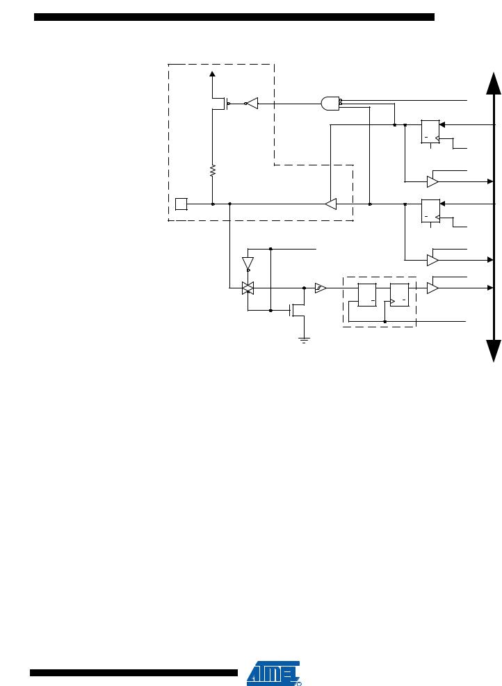
Sources” on page 25) after releasing the Reset Register. The output from this Data Register is not latched, so the reset will take place immediately, as shown in Figure 24-2.
Figure 24-2. Reset Register
To
TDO
From other Internal and
External Reset Sources
From |
Internal Reset |
D |
Q |
TDI |
|
ClockDR · AVR_RESET
24.3.4Boundary-scan Chain
The Boundary-scan Chain has the capability of driving and observing the logic levels on the digital I/O pins, as well as the boundary between digital and analog logic for analog circuitry having Off-chip connections.
See “Boundary-scan Chain” on page 235 for a complete description.
24.4Boundary-scan Specific JTAG Instructions
The instruction register is 4-bit wide, supporting up to 16 instructions. Listed below are the JTAG instructions useful for Boundary-scan operation. Note that the optional HIGHZ instruction is not implemented, but all outputs with tri-state capability can be set in high-impedant state by using the AVR_RESET instruction, since the initial state for all port pins is tri-state.
As a definition in this datasheet, the LSB is shifted in and out first for all Shift Registers.
The OPCODE for each instruction is shown behind the instruction name in hex format. The text describes which Data Register is selected as path between TDI and TDO for each instruction.
24.4.1EXTEST; $0
Mandatory JTAG instruction for selecting the Boundary-scan Chain as Data Register for testing circuitry external to the AVR package. For port-pins, Pull-up Disable, Output Control, Output Data, and Input Data are all accessible in the scan chain. For Analog circuits having Off-chip connections, the interface between the analog and the digital logic is in the scan chain. The contents of the latched outputs of the Boundary-scan chain is driven out as soon as the JTAG IRregister is loaded with the EXTEST instruction.
The active states are:
•Capture-DR: Data on the external pins are sampled into the Boundary-scan Chain.
•Shift-DR: The Internal Scan Chain is shifted by the TCK input.
•Update-DR: Data from the scan chain is applied to output pins.
234 ATmega16A 
8154A–AVR–06/08

 ATmega16A
24.4.2IDCODE; $1
Optional JTAG instruction selecting the 32-bit ID-register as Data Register. The ID-register consists of a version number, a device number and the manufacturer code chosen by JEDEC. This is the default instruction after power-up.
The active states are:
•Capture-DR: Data in the IDCODE-register is sampled into the Boundary-scan Chain.
•Shift-DR: The IDCODE scan chain is shifted by the TCK input.
24.4.3SAMPLE_PRELOAD; $2
Mandatory JTAG instruction for pre-loading the output latches and talking a snap-shot of the input/output pins without affecting the system operation. However, the output latches are not connected to the pins. The Boundary-scan Chain is selected as Data Register.
The active states are:
•Capture-DR: Data on the external pins are sampled into the Boundary-scan Chain.
•Shift-DR: The Boundary-scan Chain is shifted by the TCK input.
•Update-DR: Data from the Boundary-scan Chain is applied to the output latches. However, the output latches are not connected to the pins.
24.4.4AVR_RESET; $C
The AVR specific public JTAG instruction for forcing the AVR device into the Reset mode or releasing the JTAG Reset source. The TAP controller is not reset by this instruction. The one bit Reset Register is selected as Data Register. Note that the reset will be active as long as there is a logic 'one' in the Reset Chain. The output from this chain is not latched.
The active states are:
• Shift-DR: The Reset Register is shifted by the TCK input.
24.4.5BYPASS; $F
Mandatory JTAG instruction selecting the Bypass Register for Data Register.
The active states are:
•Capture-DR: Loads a logic “0” into the Bypass Register.
•Shift-DR: The Bypass Register cell between TDI and TDO is shifted.
24.5Boundary-scan Chain
The Boundary-scan chain has the capability of driving and observing the logic levels on the digital I/O pins, as well as the boundary between digital and analog logic for analog circuitry having Off-chip connection.
24.5.1Scanning the Digital Port Pins
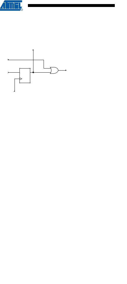
Figure 24-3 shows the Boundary-scan Cell for a bi-directional port pin with pull-up function. The cell consists of a standard Boundary-scan cell for the Pull-up Enable – PUExn – function, and a bi-directional pin cell that combines the three signals Output Control – OCxn, Output Data – ODxn, and Input Data – IDxn, into only a two-stage Shift Register. The port and pin indexes are not used in the following description.
235
8154A–AVR–06/08
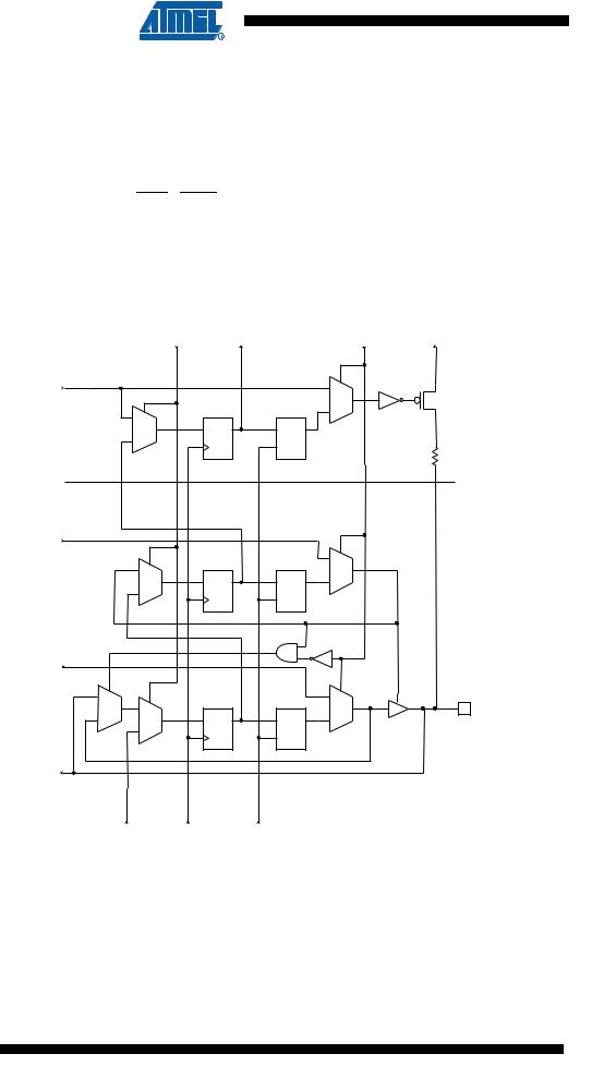
The Boundary-scan logic is not included in the figures in the datasheet. Figure 24-4 shows a simple digital Port Pin as described in the section “I/O Ports” on page 49. The Boundary-scan details from Figure 24-3 replaces the dashed box in Figure 24-4.
When no alternate port function is present, the Input Data – ID – corresponds to the PINxn Register value (but ID has no synchronizer), Output Data corresponds to the PORT Register, Output Control corresponds to the Data Direction – DD Register, and the Pull-up Enable – PUExn – corresponds to logic expression PUD · DDxn · PORTxn.
Digital alternate port functions are connected outside the dotted box in Figure 24-4 to make the scan chain read the actual pin value. For Analog function, there is a direct connection from the external pin to the analog circuit, and a scan chain is inserted on the interface between the digital logic and the analog circuitry.
Figure 24-3. Boundary-scan Cell for Bidirectional Port Pin with Pull-up Function.
ShiftDR |
To Next Cell |
EXTEST |
Vcc |
Pullup Enable (PUE) |
|
|
|
|
0 |
|
|
|
|
|
|
||
|
FF2 |
LD2 |
1 |
|||
|
0 |
|
|
|
||
|
|
|
|
|
||
|
D |
Q |
D |
Q |
|
|
|
1 |
|
G |
|
|
|
|
|
|
|
|
||
Output Control (OC) |
|
|
|
|
|
|
|
FF1 |
LD1 |
0 |
|||
|
0 |
|
|
|
1 |
|
|
D |
Q |
D |
Q |
||
|
|
|||||
|
1 |
|
G |
|
|
|
|
|
|
|
|
||
Output Data (OD) |
|
|
|
|
|
|
0 |
FF0 |
LD0 |
0 |
|||
|
0 |
|
|
|
Port Pin (PXn) |
|
1 |
|
|
|
1 |
||
D |
Q |
D |
Q |
|||
|
|
|||||
|
1 |
|
G |
|
|
|
|
|
|
|
|
||
Input Data (ID) |
|
|
|
|
|
|
From Last Cell |
ClockDR |
UpdateDR |
236 ATmega16A
8154A–AVR–06/08
ATmega16A
Figure 24-4. General Port Pin Schematic Diagram(1)
PUExn |
PUD |
|
|
|
Q D |
|
DDxn |
|
Q CLR |
|
WDx |
|
RESET |
|
OCxn |
|
RDx |
Pxn |
|
ODxn |
Q D |
|
|
|
PORTxn |
||
|
|
|
|
Q CLR |
IDxn |
|
|
|
WPx |
|
|
|
|
RESET |
|
SLEEP |
|
|
RRx |
|
|
SYNCHRONIZER |
||
|
|
|
|
RPx |
|
|
D |
Q |
D Q |
|
|
|
|
PINxn |
|
|
L |
Q |
Q |
|
|
|
|
CLK I/O |
PUD: |
PULLUP DISABLE |
WDx: |
WRITE DDRx |
|
PUExn: |
PULLUP ENABLE for pin Pxn |
RDx: |
READ DDRx |
|
OCxn: |
OUTPUT CONTROL for pin Pxn |
WPx: |
WRITE PORTx |
|
ODxn: |
OUTPUT DATA to pin Pxn |
RRx: |
READ PORTx REGISTER |
|
IDxn: |
INPUT DATA from pin Pxn |
RPx: |
READ PORTx PIN |
|
SLEEP: |
SLEEP CONTROL |
CLK I/O : |
I/O CLOCK |
|
DATA BUS
Note: 1. See Boundary-scan description for details.
24.5.2Boundary-scan and the Two-wire Interface
The 2 Two-wire Interface pins SCL and SDA have one additional control signal in the scanchain; Two-wire Interface Enable – TWIEN. As shown in Figure 24-5, the TWIEN signal enables a tri-state buffer with slew-rate control in parallel with the ordinary digital port pins. A general scan cell as shown in Figure 24-9 is attached to the TWIEN signal.
Notes: 1. A separate scan chain for the 50 ns spike filter on the input is not provided. The ordinary scan support for digital port pins suffice for connectivity tests. The only reason for having TWIEN in the scan path, is to be able to disconnect the slew-rate control buffer when doing boundaryscan.
2.Make sure the OC and TWIEN signals are not asserted simultaneously, as this will lead to drive contention.
237
8154A–AVR–06/08