

- •Features
- •1. Pin Configurations
- •2. Overview
- •2.1 Block Diagram
- •2.2 Pin Descriptions
- •2.2.3 Port A (PA7:PA0)
- •2.2.4 Port B (PB7:PB0)
- •2.2.5 Port C (PC7:PC0)
- •2.2.6 Port D (PD7:PD0)
- •2.2.7 RESET
- •2.2.8 XTAL1
- •2.2.9 XTAL2
- •2.2.10 AVCC
- •2.2.11 AREF
- •3. Resources
- •4. Data Retention
- •5. About Code Examples
- •6.1 Overview
- •6.3 Status Register
- •6.3.1 SREG – AVR Status Register
- •6.4 General Purpose Register File
- •6.5 Stack Pointer
- •6.5.1 SPH and SPL – Stack Pointer High and Low Register
- •6.6 Instruction Execution Timing
- •6.7 Reset and Interrupt Handling
- •6.7.1 Interrupt Response Time
- •7. AVR Memories
- •7.1 Overview
- •7.3 SRAM Data Memory
- •7.3.1 Data Memory Access Times
- •7.4 EEPROM Data Memory
- •7.4.1 EEPROM Read/Write Access
- •7.4.3 Preventing EEPROM Corruption
- •7.5 I/O Memory
- •7.6 Register Description
- •7.6.1 EEARH and EEARL – The EEPROM Address Register
- •7.6.2 EEDR – The EEPROM Data Register
- •7.6.3 EECR – The EEPROM Control Register
- •8. System Clock and Clock Options
- •8.1 Clock Systems and their Distribution
- •8.2 Clock Sources
- •8.3 Default Clock Source
- •8.4 Crystal Oscillator
- •8.6 External RC Oscillator
- •8.7 Calibrated Internal RC Oscillator
- •8.8 External Clock
- •8.9 Timer/Counter Oscillator
- •8.10 Register Description
- •8.10.1 OSCCAL – Oscillator Calibration Register
- •9. Power Management and Sleep Modes
- •9.1 Overview
- •9.2 Sleep Modes
- •9.3 Idle Mode
- •9.4 ADC Noise Reduction Mode
- •9.7 Standby Mode
- •9.8 Extended Standby Mode
- •9.9 Minimizing Power Consumption
- •9.9.1 Analog to Digital Converter
- •9.9.2 Analog Comparator
- •9.9.4 Internal Voltage Reference
- •9.9.5 Watchdog Timer
- •9.9.6 Port Pins
- •9.10 Register Description
- •9.10.1 MCUCR – MCU Control Register
- •10. System Control and Reset
- •10.1 Resetting the AVR
- •10.1.1 Reset Sources
- •10.1.3 External Reset
- •10.1.5 Watchdog Reset
- •10.2 Internal Voltage Reference
- •10.3 Watchdog Timer
- •10.4 Register Description
- •10.4.1 MCUCSR – MCU Control and Status Register
- •10.4.2 WDTCR – Watchdog Timer Control Register
- •11. Interrupts
- •11.1 Overview
- •11.2 Interrupt Vectors
- •11.2.1 Moving Interrupts Between Application and Boot Space
- •11.2.2 GICR – General Interrupt Control Register
- •12. I/O Ports
- •12.1 Overview
- •12.2 Ports as General Digital I/O
- •12.2.1 Configuring the Pin
- •12.2.2 Reading the Pin Value
- •12.2.3 Digital Input Enable and Sleep Modes
- •12.2.4 Unconnected pins
- •12.3 Alternate Port Functions
- •12.3.1 Alternate Functions of Port A
- •12.3.2 Alternate Functions of Port B
- •12.3.3 Alternate Functions of Port C
- •12.3.4 Alternate Functions of Port D
- •12.4 Register Description
- •12.4.1 SFIOR – Special Function I/O Register
- •12.4.2 PORTA – Port A Data Register
- •12.4.3 DDRA – Port A Data Direction Register
- •12.4.4 PINA – Port A Input Pins Address
- •12.4.5 PORTB – Port B Data Register
- •12.4.6 DDRB – Port B Data Direction Register
- •12.4.7 PINB – Port B Input Pins Address
- •12.4.8 PORTC – Port C Data Register
- •12.4.9 DDRC – Port C Data Direction Register
- •12.4.10 PINC – Port C Input Pins Address
- •12.4.11 PORTD – Port D Data Register
- •12.4.12 DDRD – Port D Data Direction Register
- •12.4.13 PIND – Port D Input Pins Address
- •13. External Interrupts
- •13.1 Register Description
- •13.1.1 MCUCR – MCU Control Register
- •13.1.2 MCUCSR – MCU Control and Status Register
- •13.1.3 GICR – General Interrupt Control Register
- •13.1.4 GIFR – General Interrupt Flag Register
- •14. 8-bit Timer/Counter0 with PWM
- •14.1 Features
- •14.2 Overview
- •14.2.1 Registers
- •14.2.2 Definitions
- •14.3 Timer/Counter Clock Sources
- •14.4 Counter Unit
- •14.5 Output Compare Unit
- •14.5.1 Force Output Compare
- •14.5.2 Compare Match Blocking by TCNT0 Write
- •14.5.3 Using the Output Compare Unit
- •14.6 Compare Match Output Unit
- •14.6.1 Compare Output Mode and Waveform Generation
- •14.7 Modes of Operation
- •14.7.1 Normal Mode
- •14.7.2 Clear Timer on Compare Match (CTC) Mode
- •14.7.3 Fast PWM Mode
- •14.7.4 Phase Correct PWM Mode
- •14.8 Timer/Counter Timing Diagrams
- •14.9 Register Description
- •14.9.1 TCCR0 – Timer/Counter Control Register
- •14.9.2 TCNT0 – Timer/Counter Register
- •14.9.3 OCR0 – Output Compare Register
- •14.9.4 TIMSK – Timer/Counter Interrupt Mask Register
- •14.9.5 TIFR qP Timer/Counter Interrupt Flag Register
- •15. Timer/Counter0 and Timer/Counter1 Prescalers
- •15.1 Overview
- •15.2 Internal Clock Source
- •15.3 Prescaler Reset
- •15.4 External Clock Source
- •15.5 Register Description
- •15.5.1 SFIOR – Special Function IO Register
- •16. 16-bit Timer/Counter1
- •16.1 Features
- •16.2 Overview
- •16.2.1 Registers
- •16.2.2 Definitions
- •16.2.3 Compatibility
- •16.3.1 Reusing the Temporary High Byte Register
- •16.4 Timer/Counter Clock Sources
- •16.5 Counter Unit
- •16.6 Input Capture Unit
- •16.6.1 Input Capture Pin Source
- •16.6.2 Noise Canceler
- •16.6.3 Using the Input Capture Unit
- •16.7 Output Compare Units
- •16.7.1 Force Output Compare
- •16.7.2 Compare Match Blocking by TCNT1 Write
- •16.7.3 Using the Output Compare Unit
- •16.8 Compare Match Output Unit
- •16.8.1 Compare Output Mode and Waveform Generation
- •16.9 Modes of Operation
- •16.9.1 Normal Mode
- •16.9.2 Clear Timer on Compare Match (CTC) Mode
- •16.9.3 Fast PWM Mode
- •16.9.4 Phase Correct PWM Mode
- •16.9.5 Phase and Frequency Correct PWM Mode
- •16.10 Timer/Counter Timing Diagrams
- •16.11 Register Description
- •16.11.1 TCCR1A – Timer/Counter1 Control Register A
- •16.11.2 TCCR1B – Timer/Counter1 Control Register B
- •16.11.4 OCR1AH and OCR1AL – Output Compare Register 1 A
- •16.11.5 OCR1BH and OCR1BL – Output Compare Register 1 B
- •16.11.6 ICR1H and ICR1L – Input Capture Register 1
- •16.11.8 TIFR – Timer/Counter Interrupt Flag Register
- •17. 8-bit Timer/Counter2 with PWM and Asynchronous Operation
- •17.1 Features
- •17.2 Overview
- •17.2.1 Registers
- •17.2.2 Definitions
- •17.3 Timer/Counter Clock Sources
- •17.4 Counter Unit
- •17.5 Output Compare Unit
- •17.5.1 Force Output Compare
- •17.5.2 Compare Match Blocking by TCNT2 Write
- •17.5.3 Using the Output Compare Unit
- •17.6 Compare Match Output Unit
- •17.6.1 Compare Output Mode and Waveform Generation
- •17.7 Modes of Operation
- •17.7.1 Normal Mode
- •17.7.2 Clear Timer on Compare Match (CTC) Mode
- •17.7.3 Fast PWM Mode
- •17.7.4 Phase Correct PWM Mode
- •17.8 Timer/Counter Timing Diagrams
- •17.9 Asynchronous Operation of the Timer/Counter2
- •17.10 Timer/Counter Prescaler
- •17.11 Register Description
- •17.11.1 TCCR2 – Timer/Counter Control Register
- •17.11.2 TCNT2 – Timer/Counter Register
- •17.11.3 OCR2 – Output Compare Register
- •17.11.4 ASSR – Asynchronous Status Register
- •17.11.5 TIMSK – Timer/Counter Interrupt Mask Register
- •17.11.6 TIFR – Timer/Counter Interrupt Flag Register
- •17.11.7 SFIOR – Special Function IO Register
- •18. SPI – Serial Peripheral Interface
- •18.1 Features
- •18.2 Overview
- •18.3 SS Pin Functionality
- •18.3.1 Slave Mode
- •18.3.2 Master Mode
- •18.4 Data Modes
- •18.5 Register Description
- •18.5.1 SPCR – SPI Control Register
- •18.5.2 SPSR – SPI Status Register
- •18.5.3 SPDR – SPI Data Register
- •19. USART
- •19.1 Features
- •19.2 Overview
- •19.2.1 AVR USART vs. AVR UART – Compatibility
- •19.3 Clock Generation
- •19.3.1 Internal Clock Generation – The Baud Rate Generator
- •19.3.2 Double Speed Operation (U2X)
- •19.3.3 External Clock
- •19.3.4 Synchronous Clock Operation
- •19.4 Frame Formats
- •19.4.1 Parity Bit Calculation
- •19.5 USART Initialization
- •19.6 Data Transmission – The USART Transmitter
- •19.6.1 Sending Frames with 5 to 8 Data Bit
- •19.6.2 Sending Frames with 9 Data Bit
- •19.6.3 Transmitter Flags and Interrupts
- •19.6.4 Parity Generator
- •19.6.5 Disabling the Transmitter
- •19.7 Data Reception – The USART Receiver
- •19.7.1 Receiving Frames with 5 to 8 Data Bits
- •19.7.2 Receiving Frames with 9 Databits
- •19.7.3 Receive Compete Flag and Interrupt
- •19.7.4 Receiver Error Flags
- •19.7.5 Parity Checker
- •19.7.6 Disabling the Receiver
- •19.7.7 Flushing the Receive Buffer
- •19.8 Asynchronous Data Reception
- •19.8.1 Asynchronous Clock Recovery
- •19.8.2 Asynchronous Data Recovery
- •19.8.3 Asynchronous Operational Range
- •19.9.1 Using MPCM
- •19.10 Accessing UBRRH/ UCSRC Registers
- •19.10.1 Write Access
- •19.10.2 Read Access
- •19.10.3 Register Description
- •19.10.4 UDR – USART I/O Data Register
- •19.10.5 UCSRA – USART Control and Status Register A
- •19.10.6 UCSRB – USART Control and Status Register B
- •19.10.7 UCSRC – USART Control and Status Register C
- •19.10.8 UBRRL and UBRRH – USART Baud Rate Registers
- •19.11 Examples of Baud Rate Setting
- •20. Two-wire Serial Interface
- •20.1 Features
- •20.2.1 TWI Terminology
- •20.2.2 Electrical Interconnection
- •20.3 Data Transfer and Frame Format
- •20.3.1 Transferring Bits
- •20.3.2 START and STOP Conditions
- •20.3.3 Address Packet Format
- •20.3.4 Data Packet Format
- •20.3.5 Combining Address and Data Packets into a Transmission
- •20.5 Overview of the TWI Module
- •20.5.1 SCL and SDA Pins
- •20.5.2 Bit Rate Generator Unit
- •20.5.3 Bus Interface Unit
- •20.5.4 Address Match Unit
- •20.5.5 Control Unit
- •20.6 Using the TWI
- •20.7 Transmission Modes
- •20.7.1 Master Transmitter Mode
- •20.7.2 Master Receiver Mode
- •20.7.3 Slave Receiver Mode
- •20.7.4 Slave Transmitter Mode
- •20.7.5 Miscellaneous States
- •20.7.6 Combining Several TWI Modes
- •20.9 Register Description
- •20.9.1 TWBR – TWI Bit Rate Register
- •20.9.2 TWCR – TWI Control Register
- •20.9.3 TWSR – TWI Status Register
- •20.9.4 TWDR – TWI Data Register
- •20.9.5 TWA R– TWI (Slave) Address Register
- •21. Analog Comparator
- •21.1 Analog Comparator Multiplexed Input
- •21.2 Register Description
- •21.2.1 SFIOR – Special Function IO Register
- •21.2.2 ACSR – Analog Comparator Control and Status Register
- •22. Analog to Digital Converter
- •22.1 Features
- •22.2 Overview
- •22.3 Operation
- •22.4 Starting a Conversion
- •22.5 Prescaling and Conversion Timing
- •22.5.1 Differential Gain Channels
- •22.6 Changing Channel or Reference Selection
- •22.6.1 ADC Input Channels
- •22.6.2 ADC Voltage Reference
- •22.7 ADC Noise Canceler
- •22.7.1 Analog Input Circuitry
- •22.7.2 Analog Noise Canceling Techniques
- •22.7.3 Offset Compensation Schemes
- •22.7.4 ADC Accuracy Definitions
- •22.8 ADC Conversion Result
- •22.9 Register Description
- •22.9.1 ADMUX – ADC Multiplexer Selection Register
- •22.9.2 ADCSRA – ADC Control and Status Register A
- •22.9.3 ADCL and ADCH – The ADC Data Register
- •ADLAR = 0
- •ADLAR = 1
- •22.9.4 SFIOR – Special FunctionIO Register
- •23. JTAG Interface and On-chip Debug System
- •23.1 Features
- •23.2 Overview
- •23.3 TAP – Test Access Port
- •23.4 TAP Controller
- •23.7.1 PRIVATE0; $8
- •23.7.2 PRIVATE1; $9
- •23.7.3 PRIVATE2; $A
- •23.7.4 PRIVATE3; $B
- •23.8 Using the JTAG Programming Capabilities
- •23.9 Register Description
- •23.10 Bibliography
- •24. IEEE 1149.1 (JTAG) Boundary-scan
- •24.1 Features
- •24.2 Overview
- •24.3 Data Registers
- •24.3.1 Bypass Register
- •24.3.2 Device Identification Register
- •24.3.3 Reset Register
- •24.4.1 EXTEST; $0
- •24.4.2 IDCODE; $1
- •24.4.3 SAMPLE_PRELOAD; $2
- •24.4.4 AVR_RESET; $C
- •24.4.5 BYPASS; $F
- •24.5.1 Scanning the Digital Port Pins
- •24.5.3 Scanning the RESET Pin
- •24.5.4 Scanning the Clock Pins
- •24.5.5 Scanning the Analog Comparator
- •24.5.6 Scanning the ADC
- •24.8 Register Description
- •24.8.1 MCUCSR – MCU Control and Status Register
- •25. Boot Loader Support – Read-While-Write Self-Programming
- •25.1 Features
- •25.2 Overview
- •25.3 Application and Boot Loader Flash Sections
- •25.3.1 Application Section
- •25.3.2 BLS – Boot Loader Section
- •25.5 Boot Loader Lock Bits
- •25.6 Entering the Boot Loader Program
- •25.6.1 SPMCR – Store Program Memory Control Register
- •25.8.1 Performing Page Erase by SPM
- •25.8.2 Filling the Temporary Buffer (Page Loading)
- •25.8.3 Performing a Page Write
- •25.8.4 Using the SPM Interrupt
- •25.8.5 Consideration while Updating BLS
- •25.8.7 Setting the Boot Loader Lock Bits by SPM
- •25.8.8 EEPROM Write Prevents Writing to SPMCR
- •25.8.9 Reading the Fuse and Lock Bits from Software
- •25.8.10 Preventing Flash Corruption
- •25.8.11 Programming Time for Flash when using SPM
- •25.8.12 Simple Assembly Code Example for a Boot Loader
- •25.8.13 ATmega16A Boot Loader Parameters
- •26. Memory Programming
- •26.1 Program And Data Memory Lock Bits
- •26.2 Fuse Bits
- •26.2.1 Latching of Fuses
- •26.3 Signature Bytes
- •26.4 Calibration Byte
- •26.5 Page Size
- •26.6 Parallel Programming Parameters, Pin Mapping, and Commands
- •26.6.1 Signal Names
- •26.7 Parallel Programming
- •26.7.1 Enter Programming Mode
- •26.7.2 Considerations for Efficient Programming
- •26.7.3 Chip Erase
- •26.7.4 Programming the Flash
- •26.7.5 Reading the Flash
- •26.7.6 Reading the EEPROM
- •26.7.7 Programming the Fuse Low Bits
- •26.7.8 Programming the Fuse High Bits
- •26.7.9 Programming the Lock Bits
- •26.7.10 Reading the Fuse and Lock Bits
- •26.7.11 Reading the Signature Bytes
- •26.7.12 Reading the Calibration Byte
- •26.8 Serial Downloading
- •26.8.1 SPI Serial Programming Pin Mapping
- •26.8.2 SPI Serial Programming Algorithm
- •26.8.3 Data Polling Flash
- •26.8.4 Data Polling EEPROM
- •26.8.5 Serial Programming Instruction set
- •26.9 SPI Serial Programming Characteristics
- •26.10 Programming via the JTAG Interface
- •26.10.1 Programming Specific JTAG Instructions
- •26.10.2 AVR_RESET ($C)
- •26.10.3 PROG_ENABLE ($4)
- •26.10.4 PROG_COMMANDS ($5)
- •26.10.5 PROG_PAGELOAD ($6)
- •26.10.6 PROG_PAGEREAD ($7)
- •26.10.7 Data Registers
- •26.10.8 Reset Register
- •26.10.9 Programming Enable Register
- •26.10.10 Programming Command Register
- •26.10.11 Virtual Flash Page Load Register
- •26.10.12 Virtual Flash Page Read Register
- •26.10.13 Programming Algorithm
- •26.10.14 Entering Programming Mode
- •26.10.15 Leaving Programming Mode
- •26.10.16 Performing Chip Erase
- •26.10.17 Programming the Flash
- •26.10.18 Reading the Flash
- •26.10.19 Programming the EEPROM
- •26.10.20 Reading the EEPROM
- •26.10.21 Programming the Fuses
- •26.10.22 Programming the Lock Bits
- •26.10.23 Reading the Fuses and Lock Bits
- •26.10.24 Reading the Signature Bytes
- •26.10.25 Reading the Calibration Byte
- •27. Electrical Characteristics
- •27.1 Absolute Maximum Ratings*
- •27.2 DC Characteristics
- •27.3 Speed Grades
- •27.4 Clock Characteristics
- •27.4.1 External Clock Drive Waveforms
- •27.4.2 External Clock Drive
- •27.5 System and Reset Characteristics
- •27.6 External Interrupts Characteristics
- •27.8 SPI Timing Characteristics
- •27.9 ADC Characteristics
- •27.10 Parallel Programming Characteristics
- •28. Typical Characteristics
- •28.0.1 Active Supply Current
- •28.0.2 Idle Supply Current
- •28.0.5 Standby Supply Current
- •28.0.6 Pin Pullup
- •28.0.7 Pin Driver Strength
- •28.0.8 Pin Thresholds And Hysteresis
- •28.0.9 Bod Thresholds
- •28.0.10 Internal Oscillator Speed
- •28.0.11 Current Consumption Of Peripheral Units
- •28.0.12 Reset Supply Current
- •29. Register Summary
- •30. Instruction Set Summary
- •31. Ordering Information
- •32. Packaging Information
- •33. Errata
- •33.1 ATmega16A rev. N to rev. Q
- •34. Datasheet Revision History
- •Table of Contents
 ATmega16A
•After the TWI has transmitted an address byte
•After the TWI has lost arbitration
•After the TWI has been addressed by own Slave address or general call
•After the TWI has received a data byte
•After a STOP or REPEATED START has been received while still addressed as a Slave.
•When a bus error has occurred due to an illegal START or STOP condition
20.6Using the TWI
The AVR TWI is byte-oriented and interrupt based. Interrupts are issued after all bus events, like reception of a byte or transmission of a START condition. Because the TWI is interrupt-based, the application software is free to carry on other operations during a TWI byte transfer. Note that the TWI Interrupt Enable (TWIE) bit in TWCR together with the Global Interrupt Enable bit in SREG allow the application to decide whether or not assertion of the TWINT Flag should generate an interrupt request. If the TWIE bit is cleared, the application must poll the TWINT Flag in order to detect actions on the TWI bus.
When the TWINT Flag is asserted, the TWI has finished an operation and awaits application response. In this case, the TWI Status Register (TWSR) contains a value indicating the current state of the TWI bus. The application software can then decide how the TWI should behave in the next TWI bus cycle by manipulating the TWCR and TWDR Registers.
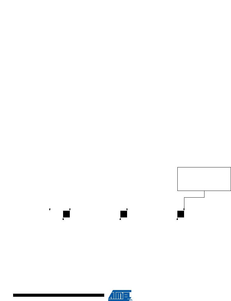
Figure 20-10 is a simple example of how the application can interface to the TWI hardware. In this example, a Master wishes to transmit a single data byte to a Slave. This description is quite abstract, a more detailed explanation follows later in this section. A simple code example implementing the desired behavior is also presented.
Figure 20-10. Interfacing the Application to the TWI in a Typical Transmission
|
1. Application |
|
3. Check TWSR to see if START was |
|
5. Check TWSR to see if SLA+W was |
||||||
|
|
|
sent. |
|
|
sent and ACK received. |
|||||
|
writes to TWCR to |
|
|
|
|
||||||
Application |
|
Application loads SLA+W into TWDR, and |
|
Application loads data into TWDR, and |
|||||||
initiate |
|
|
|||||||||
Action |
|
loads appropriate control signalsinto |
|
loads appropriate control signals into |
|||||||
transmission of |
|
|
|||||||||
|
|
TWCR, making sure that TWINT is written |
|
TWCR, making sure that TWINT is |
|||||||
|
START |
|
|
||||||||
|
|
to one, and TWSTA is written to zero |
|
|
written to one |
||||||
|
|
|
|
|
|
|
|||||
|
|
|
|
|
|
|
|
|
|
|
|
|
|
|
|
|
|
|
|
|
|
|
|
|
|
|
|
|
|
|
|
|
|
|
|
7. Check TWSR to see if data was sent and ACK received.
Application loads appropriate control signals to send STOP into TWCR, making sure that TWINT is written to one
TWI bus |
START |
|
SLA+W |
A |
|
Data |
A |
|
STOP |
|
|
|
|
|
|
|
|
|
|
|
|
|
|
|
|
|
|
|
2. TWINT set. |
||
TWI |
Status code indicates |
||
Hardware |
START condition sent |
||
Action |
|
|
|
|
|
|
|
|
|
|
|
|
Indicates |
|
|
|
|
|
|
|
|
|
|
4. TWINT set. |
|
|
|
|
|
|
|||
|
6. TWINT set. |
|
|
TWINT set |
|||||
Status code indicates |
|
|
|
||||||
|
Status code indicates |
|
|
|
|||||
SLA+W sent, ACK |
|
|
|
|
|||||
|
data sent, ACK received |
|
|
|
|||||
received |
|
|
|
|
|||||
|
|
|
|
|
|
|
|||
|
|
|
|
|
|
|
|
|
|
1.The first step in a TWI transmission is to transmit a START condition. This is done by writing a specific value into TWCR, instructing the TWI hardware to transmit a START condition. Which value to write is described later on. However, it is important that the TWINT bit is set in the value written. Writing a one to TWINT clears the flag. The TWI will not start any operation as long as the TWINT bit in TWCR is set. Immediately after
183
8154A–AVR–06/08

the application has cleared TWINT, the TWI will initiate transmission of the START condition.
2.When the START condition has been transmitted, the TWINT Flag in TWCR is set, and TWSR is updated with a status code indicating that the START condition has successfully been sent.
3.The application software should now examine the value of TWSR, to make sure that the START condition was successfully transmitted. If TWSR indicates otherwise, the application software might take some special action, like calling an error routine. Assuming that the status code is as expected, the application must load SLA+W into TWDR.
Remember that TWDR is used both for address and data. After TWDR has been loaded with the desired SLA+W, a specific value must be written to TWCR, instructing the TWI hardware to transmit the SLA+W present in TWDR. Which value to write is described later on. However, it is important that the TWINT bit is set in the value written. Writing a one to TWINT clears the flag. The TWI will not start any operation as long as the TWINT bit in TWCR is set. Immediately after the application has cleared TWINT, the TWI will initiate transmission of the address packet.
4.When the address packet has been transmitted, the TWINT Flag in TWCR is set, and TWSR is updated with a status code indicating that the address packet has successfully been sent. The status code will also reflect whether a Slave acknowledged the packet or not.
5.The application software should now examine the value of TWSR, to make sure that the address packet was successfully transmitted, and that the value of the ACK bit was as expected. If TWSR indicates otherwise, the application software might take some special action, like calling an error routine. Assuming that the status code is as expected, the application must load a data packet into TWDR. Subsequently, a specific value must be written to TWCR, instructing the TWI hardware to transmit the data packet present in TWDR. Which value to write is described later on. However, it is important that the TWINT bit is set in the value written. Writing a one to TWINT clears the flag. The TWI will not start any operation as long as the TWINT bit in TWCR is set. Immediately after the application has cleared TWINT, the TWI will initiate transmission of the data packet.
6.When the data packet has been transmitted, the TWINT Flag in TWCR is set, and TWSR is updated with a status code indicating that the data packet has successfully been sent. The status code will also reflect whether a Slave acknowledged the packet or not.
7.The application software should now examine the value of TWSR, to make sure that the data packet was successfully transmitted, and that the value of the ACK bit was as expected. If TWSR indicates otherwise, the application software might take some special action, like calling an error routine. Assuming that the status code is as expected, the application must write a specific value to TWCR, instructing the TWI hardware to transmit a STOP condition. Which value to write is described later on. However, it is important that the TWINT bit is set in the value written. Writing a one to TWINT clears the flag. The TWI will not start any operation as long as the TWINT bit in TWCR is set. Immediately after the application has cleared TWINT, the TWI will initiate transmission of the STOP condition. Note that TWINT is NOT set after a STOP condition has been sent.
Even though this example is simple, it shows the principles involved in all TWI transmissions.
These can be summarized as follows:
•When the TWI has finished an operation and expects application response, the TWINT Flag is set. The SCL line is pulled low until TWINT is cleared.
184 ATmega16A 
8154A–AVR–06/08

 ATmega16A
•When the TWINT Flag is set, the user must update all TWI Registers with the value relevant for the next TWI bus cycle. As an example, TWDR must be loaded with the value to be transmitted in the next bus cycle.
•After all TWI Register updates and other pending application software tasks have been completed, TWCR is written. When writing TWCR, the TWINT bit should be set. Writing a one to TWINT clears the flag. The TWI will then commence executing whatever operation was specified by the TWCR setting.
In the following an assembly and C implementation of the example is given. Note that the code below assumes that several definitions have been made, for example by using include-files.
|
Assembly code example |
C example |
Comments |
|
|
|
|
|
|
1 |
ldi |
r16, (1<<TWINT)|(1<<TWSTA)| |
TWCR = (1<<TWINT)|(1<<TWSTA)| |
Send START condition |
|
|
(1<<TWEN) |
(1<<TWEN) |
|
|
out |
TWCR, r16 |
|
|
2 |
wait1: |
while (!(TWCR & (1<<TWINT))) |
Wait for TWINT Flag set. This indicates |
|
|
in |
r16,TWCR |
; |
that the START condition has been |
|
sbrs |
r16,TWINT |
|
transmitted |
|
rjmp |
wait1 |
|
|
3 |
in |
r16,TWSR |
if ((TWSR & 0xF8) != START) |
Check value of TWI Status Register. Mask |
|
andi |
r16, 0xF8 |
ERROR(); |
prescaler bits. If status different from |
|
cpi |
r16, START |
|
START go to ERROR |
|
brne |
ERROR |
|
|
|
ldi |
r16, SLA_W |
TWDR = SLA_W; |
Load SLA_W into TWDR Register. Clear |
|
out |
TWDR, r16 |
TWCR = (1<<TWINT) | (1<<TWEN); |
TWINT bit in TWCR to start transmission |
|
ldi |
r16, (1<<TWINT) | (1<<TWEN) |
|
of address |
|
out |
TWCR, r16 |
|
|
4 |
wait2: |
while (!(TWCR & (1<<TWINT))) |
Wait for TWINT Flag set. This indicates |
|
|
in |
r16,TWCR |
; |
that the SLA+W has been transmitted, |
|
sbrs |
r16,TWINT |
|
and ACK/NACK has been received. |
|
rjmp |
wait2 |
|
|
5 |
in |
r16,TWSR |
if ((TWSR & 0xF8) != MT_SLA_ACK) |
Check value of TWI Status Register. Mask |
|
andi |
r16, 0xF8 |
ERROR(); |
prescaler bits. If status different from |
|
cpi |
r16, MT_SLA_ACK |
|
MT_SLA_ACK go to ERROR |
|
brne |
ERROR |
|
|
|
ldi |
r16, DATA |
TWDR = DATA; |
Load DATA into TWDR Register. Clear |
|
out |
TWDR, r16 |
TWCR = (1<<TWINT) | (1<<TWEN); |
TWINT bit in TWCR to start transmission |
|
ldi |
r16, (1<<TWINT) | (1<<TWEN) |
|
of data |
|
out |
TWCR, r16 |
|
|
6 |
wait3: |
while (!(TWCR & (1<<TWINT))) |
Wait for TWINT Flag set. This indicates |
|
|
in |
r16,TWCR |
; |
that the DATA has been transmitted, and |
|
sbrs |
r16,TWINT |
|
ACK/NACK has been received. |
|
rjmp |
wait3 |
|
|
7 |
in |
r16,TWSR |
if ((TWSR & 0xF8) != MT_DATA_ACK) |
Check value of TWI Status Register. Mask |
|
andi |
r16, 0xF8 |
ERROR(); |
prescaler bits. If status different from |
|
cpi |
r16, MT_DATA_ACK |
|
MT_DATA_ACK go to ERROR |
|
brne |
ERROR |
|
|
|
ldi |
r16, (1<<TWINT)|(1<<TWEN)| |
TWCR = (1<<TWINT)|(1<<TWEN)| |
Transmit STOP condition |
|
|
(1<<TWSTO) |
(1<<TWSTO); |
|
|
out |
TWCR, r16 |
|
|
185
8154A–AVR–06/08