

 ATmega16A
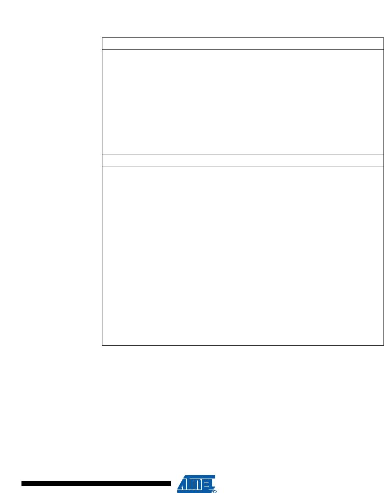
Assembly Code Example(1)
USART_Init:
; Set baud rate
out |
UBRRH, r17 |
out |
UBRRL, r16 |
; Enable receiver and transmitter |
|
ldi |
r16, (1<<RXEN)|(1<<TXEN) |
out |
UCSRB,r16 |
; Set frame format: 8data, 2stop bit |
|
ldi |
r16, (1<<URSEL)|(1<<USBS)|(3<<UCSZ0) |
out |
UCSRC,r16 |
ret |
|
C Code Example(1)
#define FOSC 1843200// Clock Speed #define BAUD 9600
#define MYUBRR FOSC/16/BAUD-1 void main( void )
{
:.
USART_Init ( MYUBRR );
:.
}
void USART_Init( unsigned int ubrr)
{
/* Set baud rate */
UBRRH = (unsigned char)(ubrr>>8);
UBRRL = (unsigned char)ubrr;
/* Enable receiver and transmitter */ UCSRB = (1<<RXEN)|(1<<TXEN);
/* Set frame format: 8data, 2stop bit */ UCSRC = (1<<URSEL)|(1<<USBS)|(3<<UCSZ0);
}
Note: 1. See “About Code Examples” on page 7.
More advanced initialization routines can be made that include frame format as parameters, disable interrupts and so on. However, many applications use a fixed setting of the Baud and Control Registers, and for these types of applications the initialization code can be placed directly in the main routine, or be combined with initialization code for other I/O modules.
19.6Data Transmission – The USART Transmitter
The USART Transmitter is enabled by setting the Transmit Enable (TXEN) bit in the UCSRB Register. When the Transmitter is enabled, the normal port operation of the TxD pin is overridden by the USART and given the function as the transmitter’s serial output. The baud rate, mode of operation and frame format must be set up once before doing any transmissions. If synchronous operation is used, the clock on the XCK pin will be overridden and used as transmission clock.
153
8154A–AVR–06/08
19.6.1Sending Frames with 5 to 8 Data Bit
A data transmission is initiated by loading the transmit buffer with the data to be transmitted. The CPU can load the transmit buffer by writing to the UDR I/O location. The buffered data in the transmit buffer will be moved to the Shift Register when the Shift Register is ready to send a new frame. The Shift Register is loaded with new data if it is in idle state (no ongoing transmission) or immediately after the last stop bit of the previous frame is transmitted. When the Shift Register is loaded with new data, it will transfer one complete frame at the rate given by the Baud Register, U2X bit or by XCK depending on mode of operation.
The following code examples show a simple USART transmit function based on polling of the Data Register Empty (UDRE) Flag. When using frames with less than eight bits, the most significant bits written to the UDR are ignored. The USART has to be initialized before the function can be used. For the assembly code, the data to be sent is assumed to be stored in Register R16
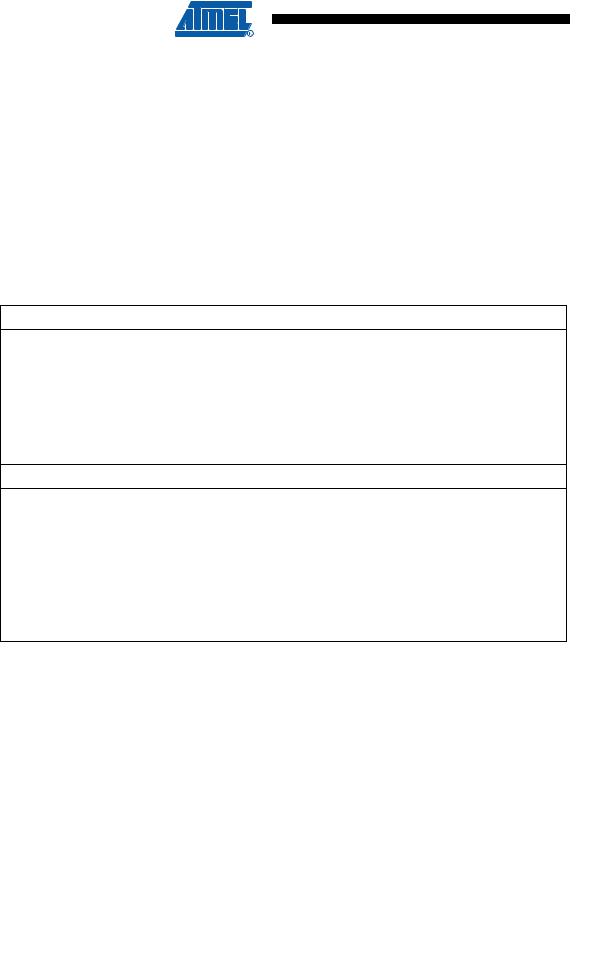
Assembly Code Example(1)
USART_Transmit:
; Wait for empty transmit buffer sbis UCSRA,UDRE
rjmp USART_Transmit
; Put data (r16) into buffer, sends the data out UDR,r16
ret
C Code Example(1)
void USART_Transmit( unsigned char data )
{
/* Wait for empty transmit buffer */ while ( !( UCSRA & (1<<UDRE)) )
;
/* Put data into buffer, sends the data */ UDR = data;
}
Note: 1. See “About Code Examples” on page 7.
The function simply waits for the transmit buffer to be empty by checking the UDRE Flag, before loading it with new data to be transmitted. If the Data Register Empty Interrupt is utilized, the interrupt routine writes the data into the buffer.
19.6.2Sending Frames with 9 Data Bit
If 9-bit characters are used (UCSZ = 7), the ninth bit must be written to the TXB8 bit in UCSRB before the Low byte of the character is written to UDR. The following code examples show a transmit function that handles 9-bit characters. For the assembly code, the data to be sent is assumed to be stored in Registers R17:R16.
154 ATmega16A 
8154A–AVR–06/08

 ATmega16A
Assembly Code Example(Note:)
USART_Transmit:
; Wait for empty transmit buffer
sbis UCSRA,UDRE rjmp USART_Transmit
; Copy 9th bit from r17 to TXB8 cbi UCSRB,TXB8
sbrc r17,0
sbi UCSRB,TXB8
; Put LSB data (r16) into buffer, sends the data out UDR,r16
ret
C Code Example(Note:)
void USART_Transmit( unsigned int data )
{
/* Wait for empty transmit buffer */ while ( !( UCSRA & (1<<UDRE))) )
;
/* Copy 9th bit to TXB8 */ UCSRB &= ~(1<<TXB8);
if ( data & 0x0100 ) UCSRB |= (1<<TXB8);
/* Put data into buffer, sends the data */ UDR = data;
}
Note: These transmit functions are written to be general functions. They can be optimized if the contents of the UCSRB is static. (i.e., only the TXB8 bit of the UCSRB Register is used after initialization).
The ninth bit can be used for indicating an address frame when using multi processor communication mode or for other protocol handling as for example synchronization.
19.6.3Transmitter Flags and Interrupts
The USART transmitter has two flags that indicate its state: USART Data Register Empty (UDRE) and Transmit Complete (TXC). Both flags can be used for generating interrupts.
The Data Register Empty (UDRE) Flag indicates whether the transmit buffer is ready to receive new data. This bit is set when the transmit buffer is empty, and cleared when the transmit buffer contains data to be transmitted that has not yet been moved into the Shift Register. For compatibility with future devices, always write this bit to zero when writing the UCSRA Register.
When the Data Register empty Interrupt Enable (UDRIE) bit in UCSRB is written to one, the USART Data Register Empty Interrupt will be executed as long as UDRE is set (provided that global interrupts are enabled). UDRE is cleared by writing UDR. When interrupt-driven data transmission is used, the Data Register Empty Interrupt routine must either write new data to UDR in order to clear UDRE or disable the Data Register empty Interrupt, otherwise a new interrupt will occur once the interrupt routine terminates.
155
8154A–AVR–06/08