

The N variable represents the prescale factor (1, 8, 32, 64, 128, 256, or 1024).
The extreme values for the OCR2 Register represent special cases when generating a PWM waveform output in the phase correct PWM mode. If the OCR2 is set equal to BOTTOM, the output will be continuously low and if set equal to MAX the output will be continuously high for noninverted PWM mode. For inverted PWM the output will have the opposite logic values.
At the very start of Period 2 in Figure 17-7 OCn has a transition from high to l ow even though there is no Compare Match. The point of this transition is to guarantee symmetry around BOTTOM. There are two cases that will give transition without Compare Match:
•OCR2A changes its value from Max, like in Figure 17-7. When the OCR2A value is MAX the OCn pin value is the same as the result of a down-counting Compare Match. To ensure symmetry around BOTTOM the OCn value at MAX must be correspond the the result of an up-counting Compare Match.
•The Timer starts counting from a value higher than the one in OCR2A, and for that reason misses the Compare Match and hence the OCn that would have happened on the way up.
17.8Timer/Counter Timing Diagrams
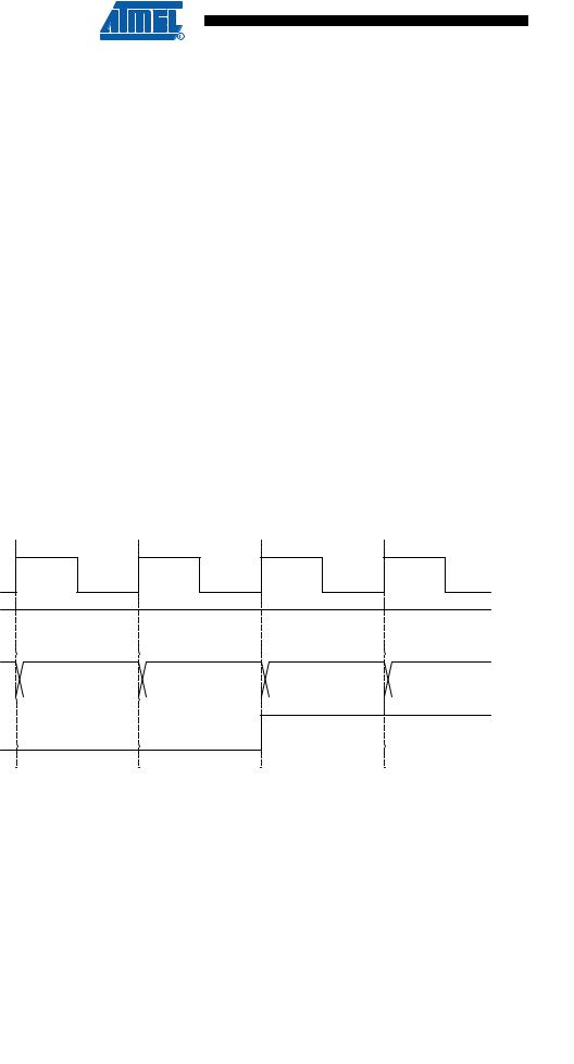
The following figures show the Timer/Counter in Synchronous mode, and the timer clock (clkT2) is therefore shown as a clock enable signal. In Asynchronous mode, clkI/O should be replaced by the Timer/Counter Oscillator clock. The figures include information on when Interrupt Flags are set. Figure 17-8 contains timing data for basic Timer/Counter operation. The figure shows the count sequence close to the MAX value in all modes other than phase correct PWM mode.
Figure 17-8. Timer/Counter Timing Diagram, no Prescaling
clkI/O
clkTn
(clkI/O/1)
TCNTn |
MAX - 1 |
|
MAX |
|
BOTTOM |
|
BOTTOM + 1 |
||
|
|
|
|
|
|
|
|
|
|
TOVn
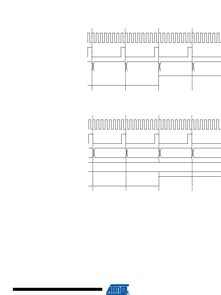
Figure 17-9 shows the same timing data, but with the prescaler enabled.
126 ATmega16A 
8154A–AVR–06/08
 ATmega16A
Figure 17-9. Timer/Counter Timing Diagram, with Prescaler (fclk_I/O/8)
clkI/O
clkTn
(clkI/O/8)
TCNTn |
MAX - 1 |
|
MAX |
|
BOTTOM |
|
BOTTOM + 1 |
||
|
|
|
|
|
|
|
|
|
|
TOVn
Figure 17-10 shows the setting of OCF2 in all modes except CTC mode.
Figure 17-10. Timer/Counter Timing Diagram, Setting of OCF2, with Prescaler (fclk_I/O/8)
clkI/O |
|
|
|
|
clkTn |
|
|
|
|
(clkI/O/8) |
|
|
|
|
TCNTn |
OCRn - 1 |
OCRn |
OCRn + 1 |
OCRn + 2 |
OCRn |
|
|
OCRn Value |
|
OCFn
Figure 17-11 shows the setting of OCF2 and the clearing of TCNT2 in CTC mode.
127
8154A–AVR–06/08
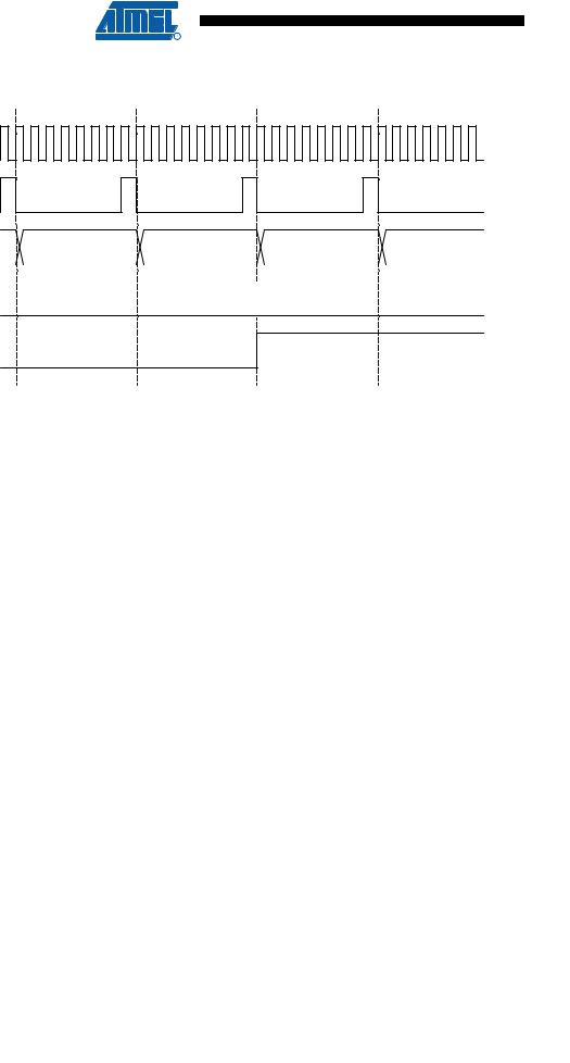
Figure 17-11.
clkI/O
clkTn
(clkI/O/8)
TCNTn
(CTC)
OCRn
OCFn
Timer/Counter Timing Diagram, Clear Timer on Compare Match Mode, with Prescaler (fclk_I/O/8)
|
|
TOP - 1 |
|
TOP |
|
BOTTOM |
|
BOTTOM + 1 |
|
|
|
|
|
|
|
|
|
|
|
|
|
|
|
|
|
|
TOP
17.9Asynchronous Operation of the Timer/Counter2
When Timer/Counter2 operates asynchronously, some considerations must be taken.
•Warning: When switching between asynchronous and synchronous clocking of Timer/Counter2, the Timer Registers TCNT2, OCR2, and TCCR2 might be corrupted. A safe procedure for switching clock source is:
1.Disable the Timer/Counter2 interrupts by clearing OCIE2 and TOIE2.
2.Select clock source by setting AS2 as appropriate.
3.Write new values to TCNT2, OCR2, and TCCR2.
4.To switch to asynchronous operation: Wait for TCN2UB, OCR2UB, and TCR2UB.
5.Clear the Timer/Counter2 Interrupt Flags.
6.Enable interrupts, if needed.
•The Oscillator is optimized for use with a 32.768 kHz watch crystal. Applying an external clock to the TOSC1 pin may result in incorrect Timer/Counter2 operation. The CPU main clock frequency must be more than four times the Oscillator frequency.
•When writing to one of the registers TCNT2, OCR2, or TCCR2, the value is transferred to a temporary register, and latched after two positive edges on TOSC1. The user should not write a new value before the contents of the temporary register have been transferred to its destination. Each of the three mentioned registers have their individual temporary register, which means for example that writing to TCNT2 does not disturb an OCR2 write in progress. To detect that a transfer to the destination register has taken place, the Asynchronous Status Register – ASSR has been implemented.
•When entering Power-save or Extended Standby mode after having written to TCNT2, OCR2, or TCCR2, the user must wait until the written register has been updated if Timer/Counter2 is used to wake up the device. Otherwise, the MCU will enter sleep mode before the changes are effective. This is particularly important if the Output Compare2 interrupt is used to wake up the device, since the output compare function is disabled during writing to OCR2 or TCNT2. If the write cycle is not finished, and the MCU enters sleep mode before the OCR2UB bit returns to zero, the device will never receive a compare match interrupt, and the MCU will not wake up.
128 ATmega16A 
8154A–AVR–06/08

 ATmega16A
•If Timer/Counter2 is used to wake the device up from Power-save or Extended Standby mode, precautions must be taken if the user wants to re-enter one of these modes: The interrupt logic needs one TOSC1 cycle to be reset. If the time between wake-up and reentering sleep mode is less than one TOSC1 cycle, the interrupt will not occur, and the device will fail to wake up. If the user is in doubt whether the time before re-entering Powersave or Extended Standby mode is sufficient, the following algorithm can be used to ensure that one TOSC1 cycle has elapsed:
1.Write a value to TCCR2, TCNT2, or OCR2.
2.Wait until the corresponding Update Busy Flag in ASSR returns to zero.
3.Enter Power-save or Extended Standby mode.
•When the asynchronous operation is selected, the 32.768 kHz Oscillator for Timer/Counter2 is always running, except in Power-down and Standby modes. After a Power-up Reset or wake-up from Power-down or Standby mode, the user should be aware of the fact that this Oscillator might take as long as one second to stabilize. The user is advised to wait for at least one second before using Timer/Counter2 after power-up or wake-up from Power-down or Standby mode. The contents of all Timer/Counter2 Registers must be considered lost after a wake-up from Power-down or Standby mode due to unstable clock signal upon start-up, no matter whether the Oscillator is in use or a clock signal is applied to the TOSC1 pin.
•Description of wake up from Power-save or Extended Standby mode when the timer is clocked asynchronously: When the interrupt condition is met, the wake up process is started on the following cycle of the timer clock, that is, the timer is always advanced by at least one before the processor can read the counter value. After wake-up, the MCU is halted for four cycles, it executes the interrupt routine, and resumes execution from the instruction following SLEEP.
•Reading of the TCNT2 Register shortly after wake-up from Power-save may give an incorrect result. Since TCNT2 is clocked on the asynchronous TOSC clock, reading TCNT2 must be done through a register synchronized to the internal I/O clock domain. Synchronization takes place for every rising TOSC1 edge. When waking up from Power-save mode, and the I/O
clock (clkI/O) again becomes active, TCNT2 will read as the previous value (before entering sleep) until the next rising TOSC1 edge. The phase of the TOSC clock after waking up from
Power-save mode is essentially unpredictable, as it depends on the wake-up time. The recommended procedure for reading TCNT2 is thus as follows:
1.Write any value to either of the registers OCR2 or TCCR2.
2.Wait for the corresponding Update Busy Flag to be cleared.
3.Read TCNT2.
•During asynchronous operation, the synchronization of the Interrupt Flags for the asynchronous timer takes three processor cycles plus one timer cycle. The timer is therefore advanced by at least one before the processor can read the timer value causing the setting of the Interrupt Flag. The output compare pin is changed on the timer clock and is not synchronized to the processor clock.
129
8154A–AVR–06/08