

- •Features
- •1. Pin Configurations
- •2. Overview
- •2.1 Block Diagram
- •2.2 Pin Descriptions
- •2.2.3 Port A (PA7:PA0)
- •2.2.4 Port B (PB7:PB0)
- •2.2.5 Port C (PC7:PC0)
- •2.2.6 Port D (PD7:PD0)
- •2.2.7 RESET
- •2.2.8 XTAL1
- •2.2.9 XTAL2
- •2.2.10 AVCC
- •2.2.11 AREF
- •3. Resources
- •4. Data Retention
- •5. About Code Examples
- •6.1 Overview
- •6.3 Status Register
- •6.3.1 SREG – AVR Status Register
- •6.4 General Purpose Register File
- •6.5 Stack Pointer
- •6.5.1 SPH and SPL – Stack Pointer High and Low Register
- •6.6 Instruction Execution Timing
- •6.7 Reset and Interrupt Handling
- •6.7.1 Interrupt Response Time
- •7. AVR Memories
- •7.1 Overview
- •7.3 SRAM Data Memory
- •7.3.1 Data Memory Access Times
- •7.4 EEPROM Data Memory
- •7.4.1 EEPROM Read/Write Access
- •7.4.3 Preventing EEPROM Corruption
- •7.5 I/O Memory
- •7.6 Register Description
- •7.6.1 EEARH and EEARL – The EEPROM Address Register
- •7.6.2 EEDR – The EEPROM Data Register
- •7.6.3 EECR – The EEPROM Control Register
- •8. System Clock and Clock Options
- •8.1 Clock Systems and their Distribution
- •8.2 Clock Sources
- •8.3 Default Clock Source
- •8.4 Crystal Oscillator
- •8.6 External RC Oscillator
- •8.7 Calibrated Internal RC Oscillator
- •8.8 External Clock
- •8.9 Timer/Counter Oscillator
- •8.10 Register Description
- •8.10.1 OSCCAL – Oscillator Calibration Register
- •9. Power Management and Sleep Modes
- •9.1 Overview
- •9.2 Sleep Modes
- •9.3 Idle Mode
- •9.4 ADC Noise Reduction Mode
- •9.7 Standby Mode
- •9.8 Extended Standby Mode
- •9.9 Minimizing Power Consumption
- •9.9.1 Analog to Digital Converter
- •9.9.2 Analog Comparator
- •9.9.4 Internal Voltage Reference
- •9.9.5 Watchdog Timer
- •9.9.6 Port Pins
- •9.10 Register Description
- •9.10.1 MCUCR – MCU Control Register
- •10. System Control and Reset
- •10.1 Resetting the AVR
- •10.1.1 Reset Sources
- •10.1.3 External Reset
- •10.1.5 Watchdog Reset
- •10.2 Internal Voltage Reference
- •10.3 Watchdog Timer
- •10.4 Register Description
- •10.4.1 MCUCSR – MCU Control and Status Register
- •10.4.2 WDTCR – Watchdog Timer Control Register
- •11. Interrupts
- •11.1 Overview
- •11.2 Interrupt Vectors
- •11.2.1 Moving Interrupts Between Application and Boot Space
- •11.2.2 GICR – General Interrupt Control Register
- •12. I/O Ports
- •12.1 Overview
- •12.2 Ports as General Digital I/O
- •12.2.1 Configuring the Pin
- •12.2.2 Reading the Pin Value
- •12.2.3 Digital Input Enable and Sleep Modes
- •12.2.4 Unconnected pins
- •12.3 Alternate Port Functions
- •12.3.1 Alternate Functions of Port A
- •12.3.2 Alternate Functions of Port B
- •12.3.3 Alternate Functions of Port C
- •12.3.4 Alternate Functions of Port D
- •12.4 Register Description
- •12.4.1 SFIOR – Special Function I/O Register
- •12.4.2 PORTA – Port A Data Register
- •12.4.3 DDRA – Port A Data Direction Register
- •12.4.4 PINA – Port A Input Pins Address
- •12.4.5 PORTB – Port B Data Register
- •12.4.6 DDRB – Port B Data Direction Register
- •12.4.7 PINB – Port B Input Pins Address
- •12.4.8 PORTC – Port C Data Register
- •12.4.9 DDRC – Port C Data Direction Register
- •12.4.10 PINC – Port C Input Pins Address
- •12.4.11 PORTD – Port D Data Register
- •12.4.12 DDRD – Port D Data Direction Register
- •12.4.13 PIND – Port D Input Pins Address
- •13. External Interrupts
- •13.1 Register Description
- •13.1.1 MCUCR – MCU Control Register
- •13.1.2 MCUCSR – MCU Control and Status Register
- •13.1.3 GICR – General Interrupt Control Register
- •13.1.4 GIFR – General Interrupt Flag Register
- •14. 8-bit Timer/Counter0 with PWM
- •14.1 Features
- •14.2 Overview
- •14.2.1 Registers
- •14.2.2 Definitions
- •14.3 Timer/Counter Clock Sources
- •14.4 Counter Unit
- •14.5 Output Compare Unit
- •14.5.1 Force Output Compare
- •14.5.2 Compare Match Blocking by TCNT0 Write
- •14.5.3 Using the Output Compare Unit
- •14.6 Compare Match Output Unit
- •14.6.1 Compare Output Mode and Waveform Generation
- •14.7 Modes of Operation
- •14.7.1 Normal Mode
- •14.7.2 Clear Timer on Compare Match (CTC) Mode
- •14.7.3 Fast PWM Mode
- •14.7.4 Phase Correct PWM Mode
- •14.8 Timer/Counter Timing Diagrams
- •14.9 Register Description
- •14.9.1 TCCR0 – Timer/Counter Control Register
- •14.9.2 TCNT0 – Timer/Counter Register
- •14.9.3 OCR0 – Output Compare Register
- •14.9.4 TIMSK – Timer/Counter Interrupt Mask Register
- •14.9.5 TIFR qP Timer/Counter Interrupt Flag Register
- •15. Timer/Counter0 and Timer/Counter1 Prescalers
- •15.1 Overview
- •15.2 Internal Clock Source
- •15.3 Prescaler Reset
- •15.4 External Clock Source
- •15.5 Register Description
- •15.5.1 SFIOR – Special Function IO Register
- •16. 16-bit Timer/Counter1
- •16.1 Features
- •16.2 Overview
- •16.2.1 Registers
- •16.2.2 Definitions
- •16.2.3 Compatibility
- •16.3.1 Reusing the Temporary High Byte Register
- •16.4 Timer/Counter Clock Sources
- •16.5 Counter Unit
- •16.6 Input Capture Unit
- •16.6.1 Input Capture Pin Source
- •16.6.2 Noise Canceler
- •16.6.3 Using the Input Capture Unit
- •16.7 Output Compare Units
- •16.7.1 Force Output Compare
- •16.7.2 Compare Match Blocking by TCNT1 Write
- •16.7.3 Using the Output Compare Unit
- •16.8 Compare Match Output Unit
- •16.8.1 Compare Output Mode and Waveform Generation
- •16.9 Modes of Operation
- •16.9.1 Normal Mode
- •16.9.2 Clear Timer on Compare Match (CTC) Mode
- •16.9.3 Fast PWM Mode
- •16.9.4 Phase Correct PWM Mode
- •16.9.5 Phase and Frequency Correct PWM Mode
- •16.10 Timer/Counter Timing Diagrams
- •16.11 Register Description
- •16.11.1 TCCR1A – Timer/Counter1 Control Register A
- •16.11.2 TCCR1B – Timer/Counter1 Control Register B
- •16.11.4 OCR1AH and OCR1AL – Output Compare Register 1 A
- •16.11.5 OCR1BH and OCR1BL – Output Compare Register 1 B
- •16.11.6 ICR1H and ICR1L – Input Capture Register 1
- •16.11.8 TIFR – Timer/Counter Interrupt Flag Register
- •17. 8-bit Timer/Counter2 with PWM and Asynchronous Operation
- •17.1 Features
- •17.2 Overview
- •17.2.1 Registers
- •17.2.2 Definitions
- •17.3 Timer/Counter Clock Sources
- •17.4 Counter Unit
- •17.5 Output Compare Unit
- •17.5.1 Force Output Compare
- •17.5.2 Compare Match Blocking by TCNT2 Write
- •17.5.3 Using the Output Compare Unit
- •17.6 Compare Match Output Unit
- •17.6.1 Compare Output Mode and Waveform Generation
- •17.7 Modes of Operation
- •17.7.1 Normal Mode
- •17.7.2 Clear Timer on Compare Match (CTC) Mode
- •17.7.3 Fast PWM Mode
- •17.7.4 Phase Correct PWM Mode
- •17.8 Timer/Counter Timing Diagrams
- •17.9 Asynchronous Operation of the Timer/Counter2
- •17.10 Timer/Counter Prescaler
- •17.11 Register Description
- •17.11.1 TCCR2 – Timer/Counter Control Register
- •17.11.2 TCNT2 – Timer/Counter Register
- •17.11.3 OCR2 – Output Compare Register
- •17.11.4 ASSR – Asynchronous Status Register
- •17.11.5 TIMSK – Timer/Counter Interrupt Mask Register
- •17.11.6 TIFR – Timer/Counter Interrupt Flag Register
- •17.11.7 SFIOR – Special Function IO Register
- •18. SPI – Serial Peripheral Interface
- •18.1 Features
- •18.2 Overview
- •18.3 SS Pin Functionality
- •18.3.1 Slave Mode
- •18.3.2 Master Mode
- •18.4 Data Modes
- •18.5 Register Description
- •18.5.1 SPCR – SPI Control Register
- •18.5.2 SPSR – SPI Status Register
- •18.5.3 SPDR – SPI Data Register
- •19. USART
- •19.1 Features
- •19.2 Overview
- •19.2.1 AVR USART vs. AVR UART – Compatibility
- •19.3 Clock Generation
- •19.3.1 Internal Clock Generation – The Baud Rate Generator
- •19.3.2 Double Speed Operation (U2X)
- •19.3.3 External Clock
- •19.3.4 Synchronous Clock Operation
- •19.4 Frame Formats
- •19.4.1 Parity Bit Calculation
- •19.5 USART Initialization
- •19.6 Data Transmission – The USART Transmitter
- •19.6.1 Sending Frames with 5 to 8 Data Bit
- •19.6.2 Sending Frames with 9 Data Bit
- •19.6.3 Transmitter Flags and Interrupts
- •19.6.4 Parity Generator
- •19.6.5 Disabling the Transmitter
- •19.7 Data Reception – The USART Receiver
- •19.7.1 Receiving Frames with 5 to 8 Data Bits
- •19.7.2 Receiving Frames with 9 Databits
- •19.7.3 Receive Compete Flag and Interrupt
- •19.7.4 Receiver Error Flags
- •19.7.5 Parity Checker
- •19.7.6 Disabling the Receiver
- •19.7.7 Flushing the Receive Buffer
- •19.8 Asynchronous Data Reception
- •19.8.1 Asynchronous Clock Recovery
- •19.8.2 Asynchronous Data Recovery
- •19.8.3 Asynchronous Operational Range
- •19.9.1 Using MPCM
- •19.10 Accessing UBRRH/ UCSRC Registers
- •19.10.1 Write Access
- •19.10.2 Read Access
- •19.10.3 Register Description
- •19.10.4 UDR – USART I/O Data Register
- •19.10.5 UCSRA – USART Control and Status Register A
- •19.10.6 UCSRB – USART Control and Status Register B
- •19.10.7 UCSRC – USART Control and Status Register C
- •19.10.8 UBRRL and UBRRH – USART Baud Rate Registers
- •19.11 Examples of Baud Rate Setting
- •20. Two-wire Serial Interface
- •20.1 Features
- •20.2.1 TWI Terminology
- •20.2.2 Electrical Interconnection
- •20.3 Data Transfer and Frame Format
- •20.3.1 Transferring Bits
- •20.3.2 START and STOP Conditions
- •20.3.3 Address Packet Format
- •20.3.4 Data Packet Format
- •20.3.5 Combining Address and Data Packets into a Transmission
- •20.5 Overview of the TWI Module
- •20.5.1 SCL and SDA Pins
- •20.5.2 Bit Rate Generator Unit
- •20.5.3 Bus Interface Unit
- •20.5.4 Address Match Unit
- •20.5.5 Control Unit
- •20.6 Using the TWI
- •20.7 Transmission Modes
- •20.7.1 Master Transmitter Mode
- •20.7.2 Master Receiver Mode
- •20.7.3 Slave Receiver Mode
- •20.7.4 Slave Transmitter Mode
- •20.7.5 Miscellaneous States
- •20.7.6 Combining Several TWI Modes
- •20.9 Register Description
- •20.9.1 TWBR – TWI Bit Rate Register
- •20.9.2 TWCR – TWI Control Register
- •20.9.3 TWSR – TWI Status Register
- •20.9.4 TWDR – TWI Data Register
- •20.9.5 TWA R– TWI (Slave) Address Register
- •21. Analog Comparator
- •21.1 Analog Comparator Multiplexed Input
- •21.2 Register Description
- •21.2.1 SFIOR – Special Function IO Register
- •21.2.2 ACSR – Analog Comparator Control and Status Register
- •22. Analog to Digital Converter
- •22.1 Features
- •22.2 Overview
- •22.3 Operation
- •22.4 Starting a Conversion
- •22.5 Prescaling and Conversion Timing
- •22.5.1 Differential Gain Channels
- •22.6 Changing Channel or Reference Selection
- •22.6.1 ADC Input Channels
- •22.6.2 ADC Voltage Reference
- •22.7 ADC Noise Canceler
- •22.7.1 Analog Input Circuitry
- •22.7.2 Analog Noise Canceling Techniques
- •22.7.3 Offset Compensation Schemes
- •22.7.4 ADC Accuracy Definitions
- •22.8 ADC Conversion Result
- •22.9 Register Description
- •22.9.1 ADMUX – ADC Multiplexer Selection Register
- •22.9.2 ADCSRA – ADC Control and Status Register A
- •22.9.3 ADCL and ADCH – The ADC Data Register
- •ADLAR = 0
- •ADLAR = 1
- •22.9.4 SFIOR – Special FunctionIO Register
- •23. JTAG Interface and On-chip Debug System
- •23.1 Features
- •23.2 Overview
- •23.3 TAP – Test Access Port
- •23.4 TAP Controller
- •23.7.1 PRIVATE0; $8
- •23.7.2 PRIVATE1; $9
- •23.7.3 PRIVATE2; $A
- •23.7.4 PRIVATE3; $B
- •23.8 Using the JTAG Programming Capabilities
- •23.9 Register Description
- •23.10 Bibliography
- •24. IEEE 1149.1 (JTAG) Boundary-scan
- •24.1 Features
- •24.2 Overview
- •24.3 Data Registers
- •24.3.1 Bypass Register
- •24.3.2 Device Identification Register
- •24.3.3 Reset Register
- •24.4.1 EXTEST; $0
- •24.4.2 IDCODE; $1
- •24.4.3 SAMPLE_PRELOAD; $2
- •24.4.4 AVR_RESET; $C
- •24.4.5 BYPASS; $F
- •24.5.1 Scanning the Digital Port Pins
- •24.5.3 Scanning the RESET Pin
- •24.5.4 Scanning the Clock Pins
- •24.5.5 Scanning the Analog Comparator
- •24.5.6 Scanning the ADC
- •24.8 Register Description
- •24.8.1 MCUCSR – MCU Control and Status Register
- •25. Boot Loader Support – Read-While-Write Self-Programming
- •25.1 Features
- •25.2 Overview
- •25.3 Application and Boot Loader Flash Sections
- •25.3.1 Application Section
- •25.3.2 BLS – Boot Loader Section
- •25.5 Boot Loader Lock Bits
- •25.6 Entering the Boot Loader Program
- •25.6.1 SPMCR – Store Program Memory Control Register
- •25.8.1 Performing Page Erase by SPM
- •25.8.2 Filling the Temporary Buffer (Page Loading)
- •25.8.3 Performing a Page Write
- •25.8.4 Using the SPM Interrupt
- •25.8.5 Consideration while Updating BLS
- •25.8.7 Setting the Boot Loader Lock Bits by SPM
- •25.8.8 EEPROM Write Prevents Writing to SPMCR
- •25.8.9 Reading the Fuse and Lock Bits from Software
- •25.8.10 Preventing Flash Corruption
- •25.8.11 Programming Time for Flash when using SPM
- •25.8.12 Simple Assembly Code Example for a Boot Loader
- •25.8.13 ATmega16A Boot Loader Parameters
- •26. Memory Programming
- •26.1 Program And Data Memory Lock Bits
- •26.2 Fuse Bits
- •26.2.1 Latching of Fuses
- •26.3 Signature Bytes
- •26.4 Calibration Byte
- •26.5 Page Size
- •26.6 Parallel Programming Parameters, Pin Mapping, and Commands
- •26.6.1 Signal Names
- •26.7 Parallel Programming
- •26.7.1 Enter Programming Mode
- •26.7.2 Considerations for Efficient Programming
- •26.7.3 Chip Erase
- •26.7.4 Programming the Flash
- •26.7.5 Reading the Flash
- •26.7.6 Reading the EEPROM
- •26.7.7 Programming the Fuse Low Bits
- •26.7.8 Programming the Fuse High Bits
- •26.7.9 Programming the Lock Bits
- •26.7.10 Reading the Fuse and Lock Bits
- •26.7.11 Reading the Signature Bytes
- •26.7.12 Reading the Calibration Byte
- •26.8 Serial Downloading
- •26.8.1 SPI Serial Programming Pin Mapping
- •26.8.2 SPI Serial Programming Algorithm
- •26.8.3 Data Polling Flash
- •26.8.4 Data Polling EEPROM
- •26.8.5 Serial Programming Instruction set
- •26.9 SPI Serial Programming Characteristics
- •26.10 Programming via the JTAG Interface
- •26.10.1 Programming Specific JTAG Instructions
- •26.10.2 AVR_RESET ($C)
- •26.10.3 PROG_ENABLE ($4)
- •26.10.4 PROG_COMMANDS ($5)
- •26.10.5 PROG_PAGELOAD ($6)
- •26.10.6 PROG_PAGEREAD ($7)
- •26.10.7 Data Registers
- •26.10.8 Reset Register
- •26.10.9 Programming Enable Register
- •26.10.10 Programming Command Register
- •26.10.11 Virtual Flash Page Load Register
- •26.10.12 Virtual Flash Page Read Register
- •26.10.13 Programming Algorithm
- •26.10.14 Entering Programming Mode
- •26.10.15 Leaving Programming Mode
- •26.10.16 Performing Chip Erase
- •26.10.17 Programming the Flash
- •26.10.18 Reading the Flash
- •26.10.19 Programming the EEPROM
- •26.10.20 Reading the EEPROM
- •26.10.21 Programming the Fuses
- •26.10.22 Programming the Lock Bits
- •26.10.23 Reading the Fuses and Lock Bits
- •26.10.24 Reading the Signature Bytes
- •26.10.25 Reading the Calibration Byte
- •27. Electrical Characteristics
- •27.1 Absolute Maximum Ratings*
- •27.2 DC Characteristics
- •27.3 Speed Grades
- •27.4 Clock Characteristics
- •27.4.1 External Clock Drive Waveforms
- •27.4.2 External Clock Drive
- •27.5 System and Reset Characteristics
- •27.6 External Interrupts Characteristics
- •27.8 SPI Timing Characteristics
- •27.9 ADC Characteristics
- •27.10 Parallel Programming Characteristics
- •28. Typical Characteristics
- •28.0.1 Active Supply Current
- •28.0.2 Idle Supply Current
- •28.0.5 Standby Supply Current
- •28.0.6 Pin Pullup
- •28.0.7 Pin Driver Strength
- •28.0.8 Pin Thresholds And Hysteresis
- •28.0.9 Bod Thresholds
- •28.0.10 Internal Oscillator Speed
- •28.0.11 Current Consumption Of Peripheral Units
- •28.0.12 Reset Supply Current
- •29. Register Summary
- •30. Instruction Set Summary
- •31. Ordering Information
- •32. Packaging Information
- •33. Errata
- •33.1 ATmega16A rev. N to rev. Q
- •34. Datasheet Revision History
- •Table of Contents
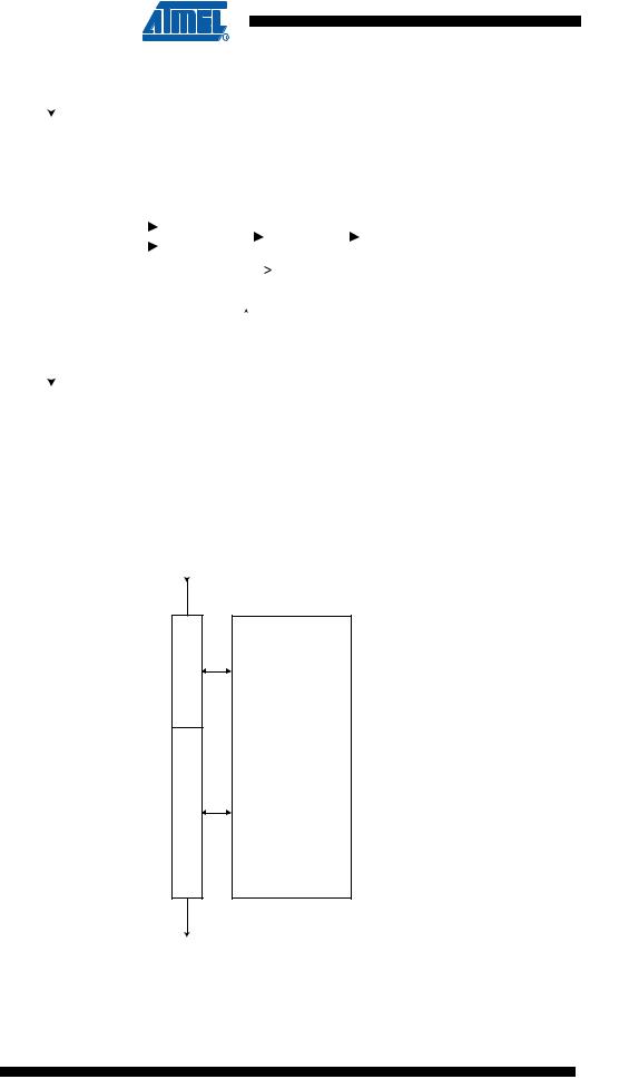
Figure 26-10. Programming Enable Register
TDI
|
|
$A370 |
|
|
|
|
|
|
|
|
|
|
|
|
|
|
|
|
|
||
D |
= |
|
|
D |
Q |
|
Programming Enable |
|||
|
|
|
|
|
||||||
A |
|
|
|
|
|
|||||
|
|
|
|
|
|
|||||
T |
|
|
|
|
|
|
|
|
|
|
|
|
|
|
|
|
|
|
|
||
A |
|
|
|
|
|
|
|
|
|
|
|
|
|
|
|
|
|
|
|
||
|
|
|
|
|
|
|
|
|
||
|
|
|
|
|
|
|
|
|
|
|
|
|
|
|
ClockDR & PROG_ENABLE |
|
|
||||
|
|
|
|
|
|
|
|
|
|
|
|
|
|
|
|
|
|
|
|
|
|
TDO
26.10.10 Programming Command Register
The Programming Command Register is a 15-bit register. This register is used to serially shift in programming commands, and to serially shift out the result of the previous command, if any. The JTAG Programming Instruction Set is shown in Table 26-14. The state sequence when shifting in the programming commands is illustrated in Figure 26-12.
Figure 26-11. Programming Command Register
TDI
S
T
R
O
B
E
S
A
D
D
R
E
S
S
/
D
A
T
A
Flash
EEPROM
Fuses
Lock Bits
TDO
284 ATmega16A
8154A–AVR–06/08

 ATmega16A
Table 26-14. JTAG Programming Instruction Set
a = address high bits, b = address low bits, H = 0 – Low byte, 1 – High Byte, o = data out, i = data in, x = don’t care
Instruction |
TDI sequence |
TDO sequence |
Notes |
|
|
|
|
|
|
1a. |
Chip erase |
0100011_10000000 |
xxxxxxx_xxxxxxxx |
|
|
|
0110001_10000000 |
xxxxxxx_xxxxxxxx |
|
|
|
0110011_10000000 |
xxxxxxx_xxxxxxxx |
|
|
|
0110011_10000000 |
xxxxxxx_xxxxxxxx |
|
|
|
|
|
|
1b. Poll for chip erase complete |
0110011_10000000 |
xxxxxox_xxxxxxxx |
(2) |
|
|
|
|
|
|
2a. |
Enter Flash Write |
0100011_00010000 |
xxxxxxx_xxxxxxxx |
|
|
|
|
|
|
2b. Load Address High Byte |
0000111_aaaaaaaa |
xxxxxxx_xxxxxxxx |
(9) |
|
|
|
|
|
|
2c. Load Address Low Byte |
0000011_bbbbbbbb |
xxxxxxx_xxxxxxxx |
|
|
|
|
|
|
|
2d. |
Load Data Low Byte |
0010011_iiiiiiii |
xxxxxxx_xxxxxxxx |
|
|
|
|
|
|
2e. |
Load Data High Byte |
0010111_iiiiiiii |
xxxxxxx_xxxxxxxx |
|
|
|
|
|
|
2f. Latch Data |
0110111_00000000 |
xxxxxxx_xxxxxxxx |
(1) |
|
|
|
1110111_00000000 |
xxxxxxx_xxxxxxxx |
|
|
|
0110111_00000000 |
xxxxxxx_xxxxxxxx |
|
|
|
|
|
|
2g. |
Write Flash Page |
0110111_00000000 |
xxxxxxx_xxxxxxxx |
(1) |
|
|
0110101_00000000 |
xxxxxxx_xxxxxxxx |
|
|
|
0110111_00000000 |
xxxxxxx_xxxxxxxx |
|
|
|
0110111_00000000 |
xxxxxxx_xxxxxxxx |
|
|
|
|
|
|
2h. |
Poll for Page Write complete |
0110111_00000000 |
xxxxxox_xxxxxxxx |
(2) |
|
|
|
|
|
3a. |
Enter Flash Read |
0100011_00000010 |
xxxxxxx_xxxxxxxx |
|
|
|
|
|
|
3b. Load Address High Byte |
0000111_aaaaaaaa |
xxxxxxx_xxxxxxxx |
(9) |
|
|
|
|
|
|
3c. Load Address Low Byte |
0000011_bbbbbbbb |
xxxxxxx_xxxxxxxx |
|
|
|
|
|
|
|
3d. |
Read Data Low and High Byte |
0110010_00000000 |
xxxxxxx_xxxxxxxx |
|
|
|
0110110_00000000 |
xxxxxxx_oooooooo |
Low byte |
|
|
0110111_00000000 |
xxxxxxx_oooooooo |
High byte |
|
|
|
|
|
4a. |
Enter EEPROM Write |
0100011_00010001 |
xxxxxxx_xxxxxxxx |
|
|
|
|
|
|
4b. Load Address High Byte |
0000111_aaaaaaaa |
xxxxxxx_xxxxxxxx |
(9) |
|
|
|
|
|
|
4c. Load Address Low Byte |
0000011_bbbbbbbb |
xxxxxxx_xxxxxxxx |
|
|
|
|
|
|
|
4d. |
Load Data Byte |
0010011_iiiiiiii |
xxxxxxx_xxxxxxxx |
|
|
|
|
|
|
4e. |
Latch Data |
0110111_00000000 |
xxxxxxx_xxxxxxxx |
(1) |
|
|
1110111_00000000 |
xxxxxxx_xxxxxxxx |
|
|
|
0110111_00000000 |
xxxxxxx_xxxxxxxx |
|
|
|
|
|
|
4f. Write EEPROM Page |
0110011_00000000 |
xxxxxxx_xxxxxxxx |
(1) |
|
|
|
0110001_00000000 |
xxxxxxx_xxxxxxxx |
|
|
|
0110011_00000000 |
xxxxxxx_xxxxxxxx |
|
|
|
0110011_00000000 |
xxxxxxx_xxxxxxxx |
|
|
|
|
|
|
4g. |
Poll for Page Write complete |
0110011_00000000 |
xxxxxox_xxxxxxxx |
(2) |
|
|
|
|
|
5a. |
Enter EEPROM Read |
0100011_00000011 |
xxxxxxx_xxxxxxxx |
|
|
|
|
|
|
5b. Load Address High Byte |
0000111_aaaaaaaa |
xxxxxxx_xxxxxxxx |
(9) |
|
|
|
|
|
|
5c. Load Address Low Byte |
0000011_bbbbbbbb |
xxxxxxx_xxxxxxxx |
|
|
|
|
|
|
|
285
8154A–AVR–06/08

Table 26-14. JTAG Programming Instruction Set (Continued)
a = address high bits, b = address low bits, H = 0 – Low byte, 1 – High Byte, o = data out, i = data in, x = don’t care
Instruction |
TDI sequence |
TDO sequence |
Notes |
|
|
|
|
|
|
5d. |
Read Data Byte |
0110011_bbbbbbbb |
xxxxxxx_xxxxxxxx |
|
|
|
0110010_00000000 |
xxxxxxx_xxxxxxxx |
|
|
|
0110011_00000000 |
xxxxxxx_oooooooo |
|
|
|
|
|
|
6a. |
Enter Fuse Write |
0100011_01000000 |
xxxxxxx_xxxxxxxx |
|
|
|
|
|
|
6b. Load Data Low Byte(6) |
0010011_iiiiiiii |
xxxxxxx_xxxxxxxx |
(3) |
|
6c. Write Fuse High byte |
0110111_00000000 |
xxxxxxx_xxxxxxxx |
(1) |
|
|
|
0110101_00000000 |
xxxxxxx_xxxxxxxx |
|
|
|
0110111_00000000 |
xxxxxxx_xxxxxxxx |
|
|
|
0110111_00000000 |
xxxxxxx_xxxxxxxx |
|
|
|
|
|
|
6d. |
Poll for Fuse Write complete |
0110111_00000000 |
xxxxxox_xxxxxxxx |
(2) |
|
|
|
|
|
6e. |
Load Data Low Byte(7) |
0010011_iiiiiiii |
xxxxxxx_xxxxxxxx |
(3) |
6f. Write Fuse Low byte |
0110011_00000000 |
xxxxxxx_xxxxxxxx |
(1) |
|
|
|
0110001_00000000 |
xxxxxxx_xxxxxxxx |
|
|
|
0110011_00000000 |
xxxxxxx_xxxxxxxx |
|
|
|
0110011_00000000 |
xxxxxxx_xxxxxxxx |
|
|
|
|
|
|
6g. |
Poll for Fuse Write complete |
0110011_00000000 |
xxxxxox_xxxxxxxx |
(2) |
|
|
|
|
|
7a. |
Enter Lock Bit Write |
0100011_00100000 |
xxxxxxx_xxxxxxxx |
|
|
|
|
|
|
7b. Load Data Byte(8) |
0010011_11iiiiii |
xxxxxxx_xxxxxxxx |
(4) |
|
7c. Write Lock Bits |
0110011_00000000 |
xxxxxxx_xxxxxxxx |
(1) |
|
|
|
0110001_00000000 |
xxxxxxx_xxxxxxxx |
|
|
|
0110011_00000000 |
xxxxxxx_xxxxxxxx |
|
|
|
0110011_00000000 |
xxxxxxx_xxxxxxxx |
|
|
|
|
|
|
7d. |
Poll for Lock Bit Write complete |
0110011_00000000 |
xxxxxox_xxxxxxxx |
(2) |
|
|
|
|
|
8a. |
Enter Fuse/Lock Bit Read |
0100011_00000100 |
xxxxxxx_xxxxxxxx |
|
|
|
|
|
|
8b. Read Fuse High Byte(6) |
0111110_00000000 |
xxxxxxx_xxxxxxxx |
|
|
|
|
0111111_00000000 |
xxxxxxx_oooooooo |
|
|
|
|
|
|
8c. Read Fuse Low Byte(7) |
0110010_00000000 |
xxxxxxx_xxxxxxxx |
|
|
|
|
0110011_00000000 |
xxxxxxx_oooooooo |
|
|
|
|
|
|
8d. |
Read Lock Bits(8) |
0110110_00000000 |
xxxxxxx_xxxxxxxx |
(5) |
|
|
0110111_00000000 |
xxxxxxx_xxoooooo |
|
|
|
|
|
|
8e. |
Read Fuses and Lock Bits |
0111110_00000000 |
xxxxxxx_xxxxxxxx |
(5) |
|
|
0110010_00000000 |
xxxxxxx_oooooooo |
Fuse High Byte |
|
|
0110110_00000000 |
xxxxxxx_oooooooo |
Fuse Low Byte |
|
|
0110111_00000000 |
xxxxxxx_oooooooo |
Lock bits |
|
|
|
|
|
9a. |
Enter Signature Byte Read |
0100011_00001000 |
xxxxxxx_xxxxxxxx |
|
|
|
|
|
|
9b. Load Address Byte |
0000011_bbbbbbbb |
xxxxxxx_xxxxxxxx |
|
|
|
|
|
|
|
9c. Read Signature Byte |
0110010_00000000 |
xxxxxxx_xxxxxxxx |
|
|
|
|
0110011_00000000 |
xxxxxxx_oooooooo |
|
|
|
|
|
|
10a. Enter Calibration Byte Read |
0100011_00001000 |
xxxxxxx_xxxxxxxx |
|
|
|
|
|
|
|
286 ATmega16A 
8154A–AVR–06/08

 ATmega16A
Table 26-14. JTAG Programming Instruction Set (Continued)
a = address high bits, b = address low bits, H = 0 – Low byte, 1 – High Byte, o = data out, i = data in, x = don’t care
Instruction |
TDI sequence |
TDO sequence |
Notes |
|
|
|
|
10b. Load Address Byte |
0000011_bbbbbbbb |
xxxxxxx_xxxxxxxx |
|
|
|
|
|
10c. Read Calibration Byte |
0110110_00000000 |
xxxxxxx_xxxxxxxx |
|
|
0110111_00000000 |
xxxxxxx_oooooooo |
|
|
|
|
|
11a. Load No Operation Command |
0100011_00000000 |
xxxxxxx_xxxxxxxx |
|
|
0110011_00000000 |
xxxxxxx_xxxxxxxx |
|
|
|
|
|
Notes: 1. This command sequence is not required if the seven MSB are correctly set by the previous command sequence (which is normally the case).
2.Repeat until o = “1”.
3.Set bits to “0” to program the corresponding fuse, “1” to unprogram the fuse.
4.Set bits to “0” to program the corresponding lock bit, “1” to leave the lock bit unchanged.
5.“0” = programmed, “1” = unprogrammed.
6.The bit mapping for Fuses High byte is listed in Table 26-3 on page 265
7.The bit mapping for Fuses Low byte is listed in Table 26-4 on page 266
8.The bit mapping for Lock bits byte is listed in Table 26-1 on page 264
9.Address bits exceeding PCMSB and EEAMSB (Table 26-5 and Table 26-6) are don’t care
287
8154A–AVR–06/08