

- •Features
- •1. Pin Configurations
- •2. Overview
- •2.1 Block Diagram
- •2.2 Pin Descriptions
- •2.2.3 Port A (PA7:PA0)
- •2.2.4 Port B (PB7:PB0)
- •2.2.5 Port C (PC7:PC0)
- •2.2.6 Port D (PD7:PD0)
- •2.2.7 RESET
- •2.2.8 XTAL1
- •2.2.9 XTAL2
- •2.2.10 AVCC
- •2.2.11 AREF
- •3. Resources
- •4. Data Retention
- •5. About Code Examples
- •6. AVR CPU Core
- •6.1 Overview
- •6.3 Status Register
- •6.3.1 SREG – AVR Status Register
- •6.4 General Purpose Register File
- •6.5 Stack Pointer
- •6.5.1 SPH and SPL – Stack Pointer High and Low Register
- •6.6 Instruction Execution Timing
- •6.7 Reset and Interrupt Handling
- •6.7.1 Interrupt Response Time
- •7. AVR Memories
- •7.1 Overview
- •7.3 SRAM Data Memory
- •7.3.1 Data Memory Access Times
- •7.4 EEPROM Data Memory
- •7.4.1 EEPROM Read/Write Access
- •7.4.3 Preventing EEPROM Corruption
- •7.5 I/O Memory
- •7.6 Register Description
- •7.6.1 EEARH and EEARL – EEPROM Address Register
- •7.6.2 EEDR – EEPROM Data Register
- •7.6.3 EECR – EEPROM Control Register
- •8. System Clock and Clock Options
- •8.1 Clock Systems and their Distribution
- •8.2 Clock Sources
- •8.3 Default Clock Source
- •8.4 Crystal Oscillator
- •8.6 External RC Oscillator
- •8.7 Calibrated Internal RC Oscillator
- •8.8 External Clock
- •8.9 Timer/Counter Oscillator
- •8.10 Register Description
- •8.10.1 OSCCAL – Oscillator Calibration Register
- •9. Power Management and Sleep Modes
- •9.1 Sleep Modes
- •9.2 Idle Mode
- •9.3 ADC Noise Reduction Mode
- •9.6 Standby Mode
- •9.7 Extended Standby Mode
- •9.8 Minimizing Power Consumption
- •9.8.1 Analog to Digital Converter
- •9.8.2 Analog Comparator
- •9.8.4 Internal Voltage Reference
- •9.8.5 Watchdog Timer
- •9.8.6 Port Pins
- •9.9 Register Description
- •9.9.1 MCUCR – MCU Control Register
- •10. System Control and Reset
- •10.1 Resetting the AVR
- •10.2 Reset Sources
- •10.2.2 External Reset
- •10.2.4 Watchdog Reset
- •10.3 Internal Voltage Reference
- •10.4 Watchdog Timer
- •10.5 Register Description
- •10.5.1 MCUCSR – MCU Control and Status Register
- •10.5.2 WDTCR – Watchdog Timer Control Register
- •11. Interrupts
- •11.1 Interrupt Vectors in ATmega32A
- •11.1.1 Moving Interrupts Between Application and Boot Space
- •11.2 Register Description
- •11.2.1 GICR – General Interrupt Control Register
- •12. I/O Ports
- •12.1 Overview
- •12.2 Ports as General Digital I/O
- •12.2.1 Configuring the Pin
- •12.2.2 Reading the Pin Value
- •12.2.3 Digital Input Enable and Sleep Modes
- •12.2.4 Unconnected pins
- •12.3 Alternate Port Functions
- •12.3.1 Alternate Functions of Port A
- •12.3.2 Alternate Functions of Port B
- •12.3.3 Alternate Functions of Port C
- •12.3.4 Alternate Functions of Port D
- •12.4 Register Description
- •12.4.1 SFIOR – Special Function I/O Register
- •12.4.2 PORTA – Port A Data Register
- •12.4.3 DDRA – Port A Data Direction Register
- •12.4.4 PINA – Port A Input Pins Address
- •12.4.5 PORTB – Port B Data Register
- •12.4.6 DDRB – Port B Data Direction Register
- •12.4.7 PINB – Port B Input Pins Address
- •12.4.8 PORTC – Port C Data Register
- •12.4.9 DDRC – Port C Data Direction Register
- •12.4.10 PINC – Port C Input Pins Address
- •12.4.11 PORTD – Port D Data Register
- •12.4.12 DDRD – Port D Data Direction Register
- •12.4.13 PIND – Port D Input Pins Address
- •13. External Interrupts
- •13.1 Register Description
- •13.1.1 MCUCR – MCU Control Register
- •13.1.2 MCUCSR – MCU Control and Status Register
- •13.1.3 GICR – General Interrupt Control Register
- •13.1.4 GIFR – General Interrupt Flag Register
- •14. 8-bit Timer/Counter0 with PWM
- •14.1 Features
- •14.2 Overview
- •14.2.1 Registers
- •14.2.2 Definitions
- •14.3 Timer/Counter Clock Sources
- •14.4 Counter Unit
- •14.5 Output Compare Unit
- •14.5.1 Force Output Compare
- •14.5.2 Compare Match Blocking by TCNT0 Write
- •14.5.3 Using the Output Compare Unit
- •14.6 Compare Match Output Unit
- •14.6.1 Compare Output Mode and Waveform Generation
- •14.7 Modes of Operation
- •14.7.1 Normal Mode
- •14.7.2 Clear Timer on Compare Match (CTC) Mode
- •14.7.3 Fast PWM Mode
- •14.7.4 Phase Correct PWM Mode
- •14.8 Timer/Counter Timing Diagrams
- •14.9 Register Description
- •14.9.1 TCCR0 – Timer/Counter Control Register
- •14.9.2 TCNT0 – Timer/Counter Register
- •14.9.3 OCR0 – Output Compare Register
- •14.9.4 TIMSK – Timer/Counter Interrupt Mask Register
- •14.9.5 TIFR – Timer/Counter Interrupt Flag Register
- •15. Timer/Counter0 and Timer/Counter1 Prescalers
- •15.1 Overview
- •15.2 Internal Clock Source
- •15.3 Prescaler Reset
- •15.4 External Clock Source
- •15.5 Register Description
- •15.5.1 SFIOR – Special Function IO Register
- •16. 16-bit Timer/Counter1
- •16.1 Features
- •16.2 Overview
- •16.2.1 Registers
- •16.2.2 Definitions
- •16.2.3 Compatibility
- •16.3.1 Reusing the Temporary High Byte Register
- •16.4 Timer/Counter Clock Sources
- •16.5 Counter Unit
- •16.6 Input Capture Unit
- •16.6.1 Input Capture Pin Source
- •16.6.2 Noise Canceler
- •16.6.3 Using the Input Capture Unit
- •16.6.4 Output Compare Units
- •16.6.5 Force Output Compare
- •16.6.6 Compare Match Blocking by TCNT1 Write
- •16.6.7 Using the Output Compare Unit
- •16.7 Compare Match Output Unit
- •16.7.1 Compare Output Mode and Waveform Generation
- •16.8 Modes of Operation
- •16.8.1 Normal Mode
- •16.8.2 Clear Timer on Compare Match (CTC) Mode
- •16.8.3 Fast PWM Mode
- •16.8.4 Phase Correct PWM Mode
- •16.8.5 Phase and Frequency Correct PWM Mode
- •16.9 Timer/Counter Timing Diagrams
- •16.10 Register Description
- •16.10.1 TCCR1A – Timer/Counter1 Control Register A
- •16.10.2 TCCR1B – Timer/Counter1 Control Register B
- •16.10.3 TCNT1H and TCNT1L – Timer/Counter1
- •16.10.4 OCR1AH and OCR1AL – Output Compare Register 1 A
- •16.10.5 OCR1BH and OCR1BL – Output Compare Register 1 B
- •16.10.6 ICR1H and ICR1L – Input Capture Register 1
- •16.10.8 TIFR – Timer/Counter Interrupt Flag Register
- •17. 8-bit Timer/Counter2 with PWM and Asynchronous Operation
- •17.1 Features
- •17.2 Overview
- •17.2.1 Registers
- •17.2.2 Definitions
- •17.3 Timer/Counter Clock Sources
- •17.4 Counter Unit
- •17.5 Output Compare Unit
- •17.5.1 Force Output Compare
- •17.5.2 Compare Match Blocking by TCNT2 Write
- •17.5.3 Using the Output Compare Unit
- •17.6 Compare Match Output Unit
- •17.6.1 Compare Output Mode and Waveform Generation
- •17.7 Modes of Operation
- •17.7.1 Normal Mode
- •17.7.2 Clear Timer on Compare Match (CTC) Mode
- •17.7.3 Fast PWM Mode
- •17.7.4 Phase Correct PWM Mode
- •17.8 Timer/Counter Timing Diagrams
- •17.9 Asynchronous Operation of the Timer/Counter
- •17.10 Timer/Counter Prescaler
- •17.11 Register Description
- •17.11.1 TCCR2 – Timer/Counter Control Register
- •17.11.2 TCNT2 – Timer/Counter Register
- •17.11.3 OCR2 – Output Compare Register
- •17.11.5 TIMSK – Timer/Counter Interrupt Mask Register
- •17.11.6 TIFR – Timer/Counter Interrupt Flag Register
- •17.11.7 SFIOR – Special Function IO Register
- •18. SPI – Serial Peripheral Interface
- •18.1 Features
- •18.2 Overview
- •18.3 SS Pin Functionality
- •18.3.1 Slave Mode
- •18.3.2 Master Mode
- •18.3.3 SPCR – SPI Control Register
- •18.3.4 SPSR – SPI Status Register
- •18.3.5 SPDR – SPI Data Register
- •18.4 Data Modes
- •19. USART
- •19.1 Features
- •19.2 Overview
- •19.2.1 AVR USART vs. AVR UART – Compatibility
- •19.3 Clock Generation
- •19.3.1 Internal Clock Generation – The Baud Rate Generator
- •19.3.2 Double Speed Operation (U2X)
- •19.3.3 External Clock
- •19.3.4 Synchronous Clock Operation
- •19.4 Frame Formats
- •19.4.1 Parity Bit Calculation
- •19.5 USART Initialization
- •19.6 Data Transmission – The USART Transmitter
- •19.6.1 Sending Frames with 5 to 8 Data Bit
- •19.6.2 Sending Frames with 9 Data Bit
- •19.6.3 Transmitter Flags and Interrupts
- •19.6.4 Parity Generator
- •19.6.5 Disabling the Transmitter
- •19.7 Data Reception – The USART Receiver
- •19.7.1 Receiving Frames with 5 to 8 Data Bits
- •19.7.2 Receiving Frames with 9 Databits
- •19.7.3 Receive Compete Flag and Interrupt
- •19.7.4 Receiver Error Flags
- •19.7.5 Parity Checker
- •19.7.6 Disabling the Receiver
- •19.7.7 Flushing the Receive Buffer
- •19.8 Asynchronous Data Reception
- •19.8.1 Asynchronous Clock Recovery
- •19.8.2 Asynchronous Data Recovery
- •19.8.3 Asynchronous Operational Range
- •19.9.1 Using MPCM
- •19.10 Accessing UBRRH/ UCSRC Registers
- •19.10.1 Write Access
- •19.10.2 Read Access
- •19.11 Register Description
- •19.11.1 UDR – USART I/O Data Register
- •19.11.2 UCSRA – USART Control and Status Register A
- •19.11.3 UCSRB – USART Control and Status Register B
- •19.11.4 UCSRC – USART Control and Status Register C
- •19.11.5 UBRRL and UBRRH – USART Baud Rate Registers
- •19.12 Examples of Baud Rate Setting
- •20. Two-wire Serial Interface
- •20.1 Features
- •20.2.1 TWI Terminology
- •20.2.2 Electrical Interconnection
- •20.3 Data Transfer and Frame Format
- •20.3.1 Transferring Bits
- •20.3.2 START and STOP Conditions
- •20.3.3 Address Packet Format
- •20.3.4 Data Packet Format
- •20.3.5 Combining Address and Data Packets into a Transmission
- •20.5 Overview of the TWI Module
- •20.5.1 SCL and SDA Pins
- •20.5.2 Bit Rate Generator Unit
- •20.5.3 Bus Interface Unit
- •20.5.4 Address Match Unit
- •20.5.5 Control Unit
- •20.6 Using the TWI
- •20.7 Transmission Modes
- •20.7.1 Master Transmitter Mode
- •20.7.2 Master Receiver Mode
- •20.7.3 Slave Receiver Mode
- •20.7.4 Slave Transmitter Mode
- •20.7.5 Miscellaneous States
- •20.7.6 Combining Several TWI Modes
- •20.9 Register Description
- •20.9.1 TWBR – TWI Bit Rate Register
- •20.9.2 TWCR – TWI Control Register
- •20.9.3 TWSR – TWI Status Register
- •20.9.4 TWDR – TWI Data Register
- •20.9.5 TWAR – TWI (Slave) Address Register
- •21. Analog Comparator
- •21.1 Overview
- •21.2 Analog Comparator Multiplexed Input
- •21.3 Register Description
- •21.3.1 SFIOR – Special Function IO Register
- •21.3.2 ACSR – Analog Comparator Control and Status Register
- •22. Analog to Digital Converter
- •22.1 Features
- •22.2 Overview
- •22.3 Operation
- •22.4 Starting a Conversion
- •22.5 Prescaling and Conversion Timing
- •22.5.1 Differential Gain Channels
- •22.6 Changing Channel or Reference Selection
- •22.6.1 ADC Input Channels
- •22.6.2 ADC Voltage Reference
- •22.7 ADC Noise Canceler
- •22.7.1 Analog Input Circuitry
- •22.7.2 Analog Noise Canceling Techniques
- •22.7.3 Offset Compensation Schemes
- •22.7.4 ADC Accuracy Definitions
- •22.8 ADC Conversion Result
- •22.9 Register Description
- •22.9.1 ADMUX – ADC Multiplexer Selection Register
- •22.9.2 ADCSRA – ADC Control and Status Register A
- •22.9.3 ADCL and ADCH – The ADC Data Register
- •22.9.4 SFIOR – Special FunctionIO Register
- •23. JTAG Interface and On-chip Debug System
- •23.1 Features
- •23.2 Overview
- •23.3 TAP – Test Access Port
- •23.4 TAP Controller
- •23.7.1 PRIVATE0; $8
- •23.7.2 PRIVATE1; $9
- •23.7.3 PRIVATE2; $A
- •23.7.4 PRIVATE3; $B
- •23.8 Using the JTAG Programming Capabilities
- •23.9 Register Description
- •23.10 Bibliography
- •24. IEEE 1149.1 (JTAG) Boundary-scan
- •24.1 Features
- •24.2 Overview
- •24.3 Data Registers
- •24.3.1 Bypass Register
- •24.3.2 Device Identification Register
- •24.3.3 Reset Register
- •24.4.1 EXTEST; $0
- •24.4.2 IDCODE; $1
- •24.4.3 SAMPLE_PRELOAD; $2
- •24.4.4 AVR_RESET; $C
- •24.4.5 BYPASS; $F
- •24.5.1 Scanning the Digital Port Pins
- •24.5.3 Scanning the RESET Pin
- •24.5.4 Scanning the Clock Pins
- •24.5.5 Scanning the Analog Comparator
- •24.5.6 Scanning the ADC
- •24.6 ATmega32A Boundary-scan Order
- •24.8 Register Description
- •24.8.1 MCU Control and Status Register – MCUCSR
- •25. Boot Loader Support – Read-While-Write Self-Programming
- •25.1 Features
- •25.2 Overview
- •25.3 Application and Boot Loader Flash Sections
- •25.3.1 Application Section
- •25.3.2 BLS – Boot Loader Section
- •25.5 Boot Loader Lock Bits
- •25.6 Entering the Boot Loader Program
- •25.8.1 Performing Page Erase by SPM
- •25.8.2 Filling the Temporary Buffer (Page Loading)
- •25.8.3 Performing a Page Write
- •25.8.4 Using the SPM Interrupt
- •25.8.5 Consideration while Updating BLS
- •25.8.7 Setting the Boot Loader Lock Bits by SPM
- •25.8.8 EEPROM Write Prevents Writing to SPMCR
- •25.8.9 Reading the Fuse and Lock Bits from Software
- •25.8.10 Preventing Flash Corruption
- •25.8.11 Programming Time for Flash when using SPM
- •25.8.12 Simple Assembly Code Example for a Boot Loader
- •25.8.13 Boot Loader Parameters
- •25.9 Register Description
- •25.9.1 SPMCR – Store Program Memory Control Register
- •26. Memory Programming
- •26.1 Program And Data Memory Lock Bits
- •26.2 Fuse Bits
- •26.2.1 Latching of Fuses
- •26.3 Signature Bytes
- •26.4 Calibration Byte
- •26.5 Page Size
- •26.6 Parallel Programming Parameters, Pin Mapping, and Commands
- •26.6.1 Signal Names
- •26.7 Parallel Programming
- •26.7.1 Enter Programming Mode
- •26.7.2 Considerations for Efficient Programming
- •26.7.3 Chip Erase
- •26.7.4 Programming the Flash
- •26.7.5 Programming the EEPROM
- •26.7.6 Reading the Flash
- •26.7.7 Reading the EEPROM
- •26.7.8 Programming the Fuse Low Bits
- •26.7.9 Programming the Fuse High Bits
- •26.7.10 Programming the Lock Bits
- •26.7.11 Reading the Fuse and Lock Bits
- •26.7.12 Reading the Signature Bytes
- •26.7.13 Reading the Calibration Byte
- •26.7.14 Parallel Programming Characteristics
- •26.8 SPI Serial Downloading
- •26.9 SPI Serial Programming Pin Mapping
- •26.9.1 SPI Serial Programming Algorithm
- •26.9.2 Data Polling Flash
- •26.9.3 Data Polling EEPROM
- •26.9.4 SPI Serial Programming Characteristics
- •26.10 Programming via the JTAG Interface
- •26.10.1 Programming Specific JTAG Instructions
- •26.10.2 AVR_RESET ($C)
- •26.10.3 PROG_ENABLE ($4)
- •26.10.4 PROG_COMMANDS ($5)
- •26.10.5 PROG_PAGELOAD ($6)
- •26.10.6 PROG_PAGEREAD ($7)
- •26.10.7 Data Registers
- •26.10.8 Reset Register
- •26.10.9 Programming Enable Register
- •26.10.10 Programming Command Register
- •26.10.11 Virtual Flash Page Load Register
- •26.10.12 Virtual Flash Page Read Register
- •26.10.13 Programming Algorithm
- •26.10.14 Entering Programming Mode
- •26.10.15 Leaving Programming Mode
- •26.10.16 Performing Chip Erase
- •26.10.17 Programming the Flash
- •26.10.18 Reading the Flash
- •26.10.19 Programming the EEPROM
- •26.10.20 Reading the EEPROM
- •26.10.21 Programming the Fuses
- •26.10.22 Programming the Lock Bits
- •26.10.23 Reading the Fuses and Lock Bits
- •26.10.24 Reading the Signature Bytes
- •26.10.25 Reading the Calibration Byte
- •27. Electrical Characteristics
- •27.1 Absolute Maximum Ratings*
- •27.2 DC Characteristics
- •27.3 Speed Grades
- •27.4 Clock Characteristics
- •27.4.1 External Clock Drive Waveforms
- •27.4.2 External Clock Drive
- •27.5 System and Reset Characteristics
- •27.7 SPI Timing Characteristics
- •27.8 ADC Characteristics
- •28. Typical Characteristics
- •28.1 Active Supply Current
- •28.2 Idle Supply Current
- •28.5 Standby Supply Current
- •28.7 Pin Driver Strength
- •28.8 Pin Thresholds and Hysteresis
- •28.9 BOD Thresholds and Analog Comparator Offset
- •28.10 Internal Oscillator Speed
- •28.11 Current Consumption of Peripheral Units
- •28.12 Current Consumption in Reset and Reset Pulsewidth
- •29. Register Summary
- •30. Instruction Set Summary
- •31. Ordering Information
- •32. Packaging Information
- •33. Errata
- •33.1 ATmega32A, rev. G to rev. I
- •34. Datasheet Revision History
- •Table of Contents

 ATmega32A
Figure 27-3. External Clock Drive
|
|
|
VCC = 2.7V to 5.5V |
VCC = 4.5V to 5.5V |
|
||||
Symbol |
Parameter |
Min |
|
Max |
Min |
Max |
Units |
||
|
|
|
|
|
|
|
|
|
|
tCLCH |
Rise Time |
|
|
1.6 |
|
|
0.5 |
μs |
|
tCHCL |
Fall Time |
|
|
1.6 |
|
|
0.5 |
μs |
|
|
Change in period from |
|
|
|
|
|
|
|
|
|
one clock cycle to the |
|
|
2 |
|
|
2 |
% |
|
tCLCL |
next |
|
|
|
|
|
|
|
|
Figure 27-4. External RC Oscillator, Typical Frequencies (VCC = 5V) |
|
|
|||||||
|
R [kΩ](1) |
|
|
C [pF] |
|
|
f(2) |
|
|
|
33 |
|
|
22 |
|
|
650 kHz |
|
|
|
|
|
|
|
|
|
|
|
|
|
10 |
|
|
22 |
|
|
2.0 MHz |
|
|
|
|
|
|
|
|
|
|
|
|
Notes: 1. R should be in the range 3 kΩ - 100 kΩ, and C should be at least 20 pF. The C values given in the table includes pin capacitance. This will vary with package type.
2.The frequency will vary with package type and board layout.
27.5System and Reset Characteristics
Table 27-1. |
Reset, Brown-out and Internal Voltage Reference Characteristics |
|
|||||||
Symbol |
|
Parameter |
Condition |
Min |
Typ |
Max |
Units |
||
|
|
|
|
|
|
|
|
||
|
|
Power-on Reset Threshold |
|
|
1.4 |
2.3 |
V |
||
|
|
Voltage (rising) |
|
|
|||||
VPOT |
|
|
|
|
|
|
|||
|
|
|
|
|
|
|
|
|
|
|
Power-on Reset Threshold |
|
|
1.3 |
2.3 |
V |
|||
|
|
|
|
||||||
|
|
Voltage (falling)(1) |
|
|
|||||
|
|
|
|
|
|
|
|||
|
|
|
|
Pin Threshold |
|
|
|
|
|
VRST |
|
RESET |
|
0.2 VCC |
|
0.9VCC |
V |
||
|
Voltage |
|
|
||||||
tRST |
|
Minimum pulse width on |
|
|
|
1.5 |
µs |
||
|
RESET |
Pin |
|
|
|
||||
VBOT |
|
Brown-out Reset Threshold |
BODLEVEL = 1 |
2.5 |
2.7 |
2.9 |
V |
||
|
Voltage(2) |
|
|
|
|
||||
|
BODLEVEL = 0 |
3.6 |
4.0 |
4.2 |
|||||
|
|
|
|
|
|
||||
|
|
|
|
|
|
|
|
||
tBOD |
|
Minimum low voltage period |
BODLEVEL = 1 |
|
2 |
|
µs |
||
|
for Brown-out Detection |
|
|
|
|
|
|||
|
BODLEVEL = 0 |
|
2 |
|
µs |
||||
|
|
|
|
|
|
|
|||
|
|
|
|
|
|
|
|
||
VHYST |
|
Brown-out Detector |
|
|
50 |
|
mV |
||
|
hysteresis |
|
|
|
|||||
|
|
|
|
|
|
|
|||
|
|
|
|
|
|
|
|
||
VBG |
|
Bandgap reference voltage |
|
1.15 |
1.23 |
1.35 |
V |
||
tBG |
|
Bandgap reference start-up |
|
|
40 |
70 |
µs |
||
|
time |
|
|
||||||
IBG |
|
Bandgap reference current |
|
|
10 |
|
µA |
||
|
consumption |
|
|
|
|||||
Notes: 1. The Power-on Reset will not work unless the supply voltage has been below VPOT (falling).
2.VBOT may be below nominal minimum operating voltage for some devices. For devices where this is the case, the device is tested down to VCC = VBOT during the production test. This guar-
299
8155B–AVR–07/09

antees that a Brown-out Reset will occur before VCC drops to a voltage where correct operation of the microcontroller is no longer guaranteed. The test is performed using BODLEVEL = 1 and BODLEVEL = 0 for ATmega32A.
27.6Two-wire Serial Interface Characteristics
Table 27-2 describes the requirements for devices connected to the Two-wire Serial Bus. The ATmega32A Two-wire Serial Interface meets or exceeds these requirements under the noted conditions.
Timing symbols refer to Figure 27-5.
Table 27-2. |
Two-wire Serial Bus Requirements |
|
|
|
|
|
|
|||||
Symbol |
|
Parameter |
|
|
|
Condition |
Min |
|
Max |
Units |
||
|
|
|
|
|
|
|
|
|
|
|
||
VIL |
|
Input Low-voltage |
|
|
|
|
-0.5 |
|
0.3 VCC |
V |
||
VIH |
|
Input High-voltage |
|
|
|
|
0.7 VCC |
VCC + 0.5 |
V |
|||
|
|
(1) |
|
Hysteresis of Schmitt Trigger Inputs |
|
|
|
|
(2) |
– |
V |
|
Vhys |
|
|
|
|
0.05 VCC |
|||||||
V |
(1) |
|
Output Low-voltage |
|
|
|
3 mA sink current |
0 |
|
0.4 |
V |
|
|
OL |
|
|
|
|
|
|
|
|
|
|
|
t |
(1) |
|
Rise Time for both SDA and SCL |
|
|
|
20 + 0.1C |
(3)(2) |
300 |
ns |
||
|
r |
|
|
|
|
|
|
|
|
b |
|
|
t |
of |
(1) |
|
Output Fall Time from V |
to V |
|
|
10 pF < C < 400 pF(3) |
20 + 0.1C |
(3)(2) |
250 |
ns |
|
|
|
IHmin |
ILmax |
|
|
b |
|
b |
|
|
|
tSP(1) |
|
Spikes Suppressed by Input Filter |
|
|
|
0 |
|
50(2) |
ns |
|||
Ii |
|
|
Input Current each I/O Pin |
|
|
|
0.1VCC < Vi < 0.9VCC |
-10 |
|
10 |
µA |
|
|
|
|
|
|
|
|
|
|
|
|
||
C |
(1) |
|
Capacitance for each I/O Pin |
|
|
|
– |
|
10 |
pF |
||
|
i |
|
|
|
|
|
|
|
|
|
|
|
f |
SCL |
|
SCL Clock Frequency |
|
f |
CK |
(4) > max(16f , 250kHz)(5) |
0 |
|
400 |
kHz |
|
|
|
|
|
|
SCL |
|
|
|
|
|||
|
|
|
|
|
|
|
|
fSCL ≤ 100 kHz |
VCC – 0,4V |
1000ns |
Ω |
|
|
|
|
|
|
|
|
|
|
---------------------------- |
------------------- |
||
Rp |
|
Value of Pull-up resistor |
|
|
|
|
3mA |
|
Cb |
|
||
|
|
|
|
fSCL > 100 kHz |
VCC – 0,4V |
300ns |
Ω |
|||||
|
|
|
|
|
|
|
|
|||||
|
|
|
|
|
|
|
|
|
---------------------------- |
--------------- |
||
|
|
|
|
|
|
|
|
|
3mA |
|
Cb |
|
tHD;STA |
|
Hold Time (repeated) START Condition |
|
|
fSCL ≤ 100 kHz |
4.0 |
|
– |
µs |
|||
|
|
|
|
|
|
|
|
|||||
|
|
|
fSCL > 100 kHz |
0.6 |
|
– |
µs |
|||||
|
|
|
|
|
|
|
|
|
||||
tLOW |
|
Low Period of the SCL Clock |
|
|
f ≤ 100 kHz(6) |
4.7 |
|
– |
µs |
|||
|
|
|
SCL |
|
|
|
|
|||||
|
|
|
|
|
|
|
|
|
|
|
|
|
|
|
|
|
|
|
|
|
fSCL > 100 kHz(7) |
1.3 |
|
– |
µs |
tHIGH |
|
High period of the SCL clock |
|
|
|
fSCL ≤ 100 kHz |
4.0 |
|
– |
µs |
||
|
|
|
|
fSCL > 100 kHz |
0.6 |
|
– |
µs |
||||
|
|
|
|
|
|
|
|
|
||||
tSU;STA |
|
|
|
|
|
fSCL ≤ 100 kHz |
4.7 |
|
– |
µs |
||
|
|
|
|
|
|
|
|
|
|
|||
|
Set-up time for a repeated START condition |
|
|
fSCL > 100 kHz |
0.6 |
|
– |
µs |
||||
|
|
|
|
|
|
|
||||||
tHD;DAT |
|
Data hold time |
|
|
|
fSCL ≤ 100 kHz |
0 |
|
3.45 |
µs |
||
|
|
|
|
fSCL > 100 kHz |
0 |
|
0.9 |
µs |
||||
|
|
|
|
|
|
|
|
|
||||
|
|
|
|
|
|
|
|
|
|
|
|
|
tSU;DAT |
|
Data setup time |
|
|
|
fSCL ≤ 100 kHz |
250 |
|
– |
ns |
||
|
|
|
|
|
|
|
|
|
||||
|
|
|
|
fSCL > 100 kHz |
100 |
|
– |
ns |
||||
|
|
|
|
|
|
|
|
|
||||
300 ATmega32A 
8155B–AVR–07/09
 ATmega32A
Table 27-2. Two-wire Serial Bus Requirements |
(Continued) |
|
|
|
||
Symbol |
Parameter |
|
Condition |
Min |
Max |
Units |
|
|
|
|
|
|
|
tSU;STO |
Setup time for STOP condition |
|
fSCL ≤ 100 kHz |
4.0 |
– |
µs |
|
fSCL > 100 kHz |
0.6 |
– |
µs |
||
|
|
|
||||
|
|
|
|
|
|
|
tBUF |
Bus free time between a STOP and START |
|
fSCL ≤ 100 kHz |
4.7 |
– |
µs |
|
|
|
|
|
||
|
condition |
|
fSCL > 100 kHz |
1.3 |
– |
µs |
Notes: 1. |
In ATmega32A, this parameter is characterized and not 100% tested. |
|
|
|
||
2.Required only for fSCL > 100 kHz.
3.Cb = capacitance of one bus line in pF.
4.fCK = CPU clock frequency
5.This requirement applies to all ATmega32A Two-wire Serial Interface operation. Other devices connected to the Two-wire Serial Bus need only obey the general fSCL requirement.
6.The actual low period generated by the ATmega32A Two-wire Serial Interface is (1/fSCL - 2/fCK), thus fCK must be greater than 6 MHz for the low time requirement to be strictly met at fSCL = 100 kHz.
7.The actual low period generated by the ATmega32A Two-wire Serial Interface is (1/fSCL - 2/fCK), thus the low time requirement will not be strictly met for fSCL > 308 kHz when fCK = 8 MHz. Still, ATmega32A devices connected to the bus may communicate at full speed (400 kHz) with other ATmega32A devices, as well as any other device with a proper tLOW acceptance margin.
Figure 27-5. Two-wire Serial Bus Timing
|
|
|
|
|
|
|
|
|
|
|
|
tof |
|
|
tHIGH |
|
|
|
|
|
|
|
|
|
|
|
|
|
|
|
|
tr |
||
|
|
|
|
|
|
|
|
|
|
|
|
|
||||||||||||||||||||||
|
|
|
|
|
|
|
|
|
|
|
|
|
|
|
|
|
|
|
|
|
||||||||||||||
SCL |
|
|
|
|
|
|
|
|
|
|
|
tLOW |
|
|
|
|
tLOW |
|
|
|
|
|
|
|
|
|
|
|
|
|
||||
|
|
|
|
|
||||||||||||||||||||||||||||||
|
|
|
|
|
|
|
|
|
|
|
|
|
||||||||||||||||||||||
|
|
|
|
|
|
|
|
|
|
|
|
|
|
|
|
|
|
|
|
|
|
|
|
|
|
|
|
|
|
|
|
|
|
|
|
|
|
|
|
|
|
|
|
|
|
|
|
|
|
|
|
|
|
|
|
|
|
|
|
|
|
|
|
|
|
|
|
|
|
tSU;STA |
|
|
|
|
|
|
|
|
|
tHD;STA |
|
tHD;DAT |
|
|
|
|
|
|
t |
|
|
|
|
|
|
|
||||||||
SDA |
|
|
|
|
|
|
|
|
|
|
|
|
|
|
|
|
|
|
|
|
|
|
SU;DAT |
|
|
|
|
tSU;STO |
||||||
|
|
|
|
|
|
|
|
|
|
|
|
|
|
|
|
|
|
|
|
|
|
|
|
|
|
|
|
|
|
|
||||
|
|
|
|
|
|
|
|
|
|
|
|
|
|
|
|
|
|
|
|
|
|
|
|
|
|
|
|
|
|
|
|
|
|
|
|
|
|
|
|
|
|
|
|
|
|
|
|
|
|
|
|
|
|
|
|
|
|
|
|
|
|
|
|
|
|
|
|
|
|
tBUF
27.7SPI Timing Characteristics
See Figure 27-6 and Figure 27-7 for details. |
|
|
|
|
|||||
Table 27-3. |
|
SPI Timing Parameters |
|
|
|
|
|||
|
|
|
|
|
|
|
|
|
|
|
|
|
Description |
Mode |
Min |
Typ |
Max |
|
|
|
|
|
|
|
|
|
|
|
|
1 |
|
|
SCK period |
Master |
|
See Table 18-4 |
|
|
|
|
|
|
|
|
|
|
|
||
2 |
|
SCK high/low |
Master |
|
50% duty cycle |
|
|
||
|
|
|
|
|
|
|
|
||
3 |
|
Rise/Fall time |
Master |
|
3.6 |
|
|
||
|
|
|
|
|
|
|
|
|
|
4 |
|
|
|
Setup |
Master |
|
10 |
|
|
|
|
|
|
|
|
|
|
|
|
5 |
|
|
|
Hold |
Master |
|
10 |
|
|
|
|
|
|
|
|
|
|
ns |
|
6 |
|
|
Out to SCK |
Master |
|
0.5 • tSCK |
|
||
7 |
|
|
SCK to out |
Master |
|
10 |
|
|
|
|
|
|
|
|
|
|
|
||
8 |
|
SCK to out high |
Master |
|
10 |
|
|
||
|
|
|
|
|
|
|
|
|
|
9 |
|
|
|
low to out |
Slave |
|
15 |
|
|
|
SS |
|
|
|
|||||
10 |
|
|
SCK period |
Slave |
4 • tck |
|
|
|
|
11 |
|
SCK high/low |
Slave |
2 • tck |
|
|
|
||
12 |
|
Rise/Fall time |
Slave |
|
|
1.6 |
µs |
||
|
|
|
|
|
|
|
|
|
|
301
8155B–AVR–07/09
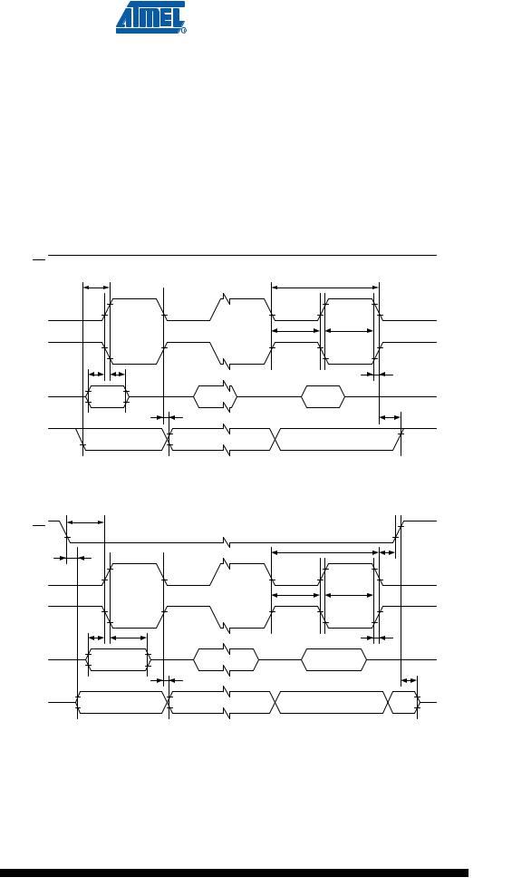
Table 27-3. |
|
|
|
|
|
|
|
|
|
|
|
|
|
|
|
|
|
|
|
|
|
|
|
|
|
|
|
|
|
|
|
||
|
|
SPI Timing Parameters |
|
|
|
|
|
|||||||||
|
|
|
|
|
|
|
|
|
|
|
|
|
|
|||
|
|
|
|
Description |
Mode |
Min |
Typ |
Max |
|
|
||||||
|
|
|
|
|
|
|
|
|
|
|
|
|
|
|
||
13 |
|
|
|
|
Setup |
Slave |
10 |
|
|
|
|
|||||
|
|
|
|
|
|
|
|
|
|
|
|
|
|
|
||
14 |
|
|
|
|
Hold |
Slave |
tck |
|
|
|
|
|||||
15 |
|
|
|
SCK to out |
Slave |
|
15 |
|
ns |
|
||||||
|
|
|
|
|
|
|
|
|
|
|
|
|
|
|
|
|
16 |
|
SCK to |
|
high |
Slave |
20 |
|
|
|
|||||||
|
SS |
|
|
|
|
|||||||||||
|
|
|
|
|
|
|
|
|
|
|
|
|
|
|||
17 |
|
|
|
high to tri-state |
Slave |
|
10 |
|
|
|
||||||
SS |
|
|
|
|
||||||||||||
18 |
|
|
|
|
low to SCK |
Salve |
2 • tck |
|
|
|
|
|||||
|
SS |
|
|
|
|
|||||||||||
Figure 27-6. SPI Interface Timing Requirements (Master Mode)
SS
SCK (CPOL = 0)
SCK (CPOL = 1)
MISO
(Data Input)
MOSI
(Data Output)
6 |
|
|
1 |
|
|
2 |
2 |
4 |
5 |
|
3 |
|
MSB |
... |
LSB |
|
|
7 |
8 |
|
MSB |
... |
LSB |
Figure 27-7. SPI Interface Timing Requirements (Slave Mode)
SS
SCK (CPOL = 0)
SCK (CPOL = 1)
MOSI
(Data Input)
MISO
(Data Output)
18 |
|
|
|
|
9 |
|
|
10 |
16 |
|
|
|
|
|
|
|
11 |
11 |
|
13 |
14 |
|
|
12 |
|
MSB |
... |
LSB |
|
|
|
15 |
|
17 |
|
MSB |
... |
LSB |
X |
302 ATmega32A
8155B–AVR–07/09