

 ATmega8A
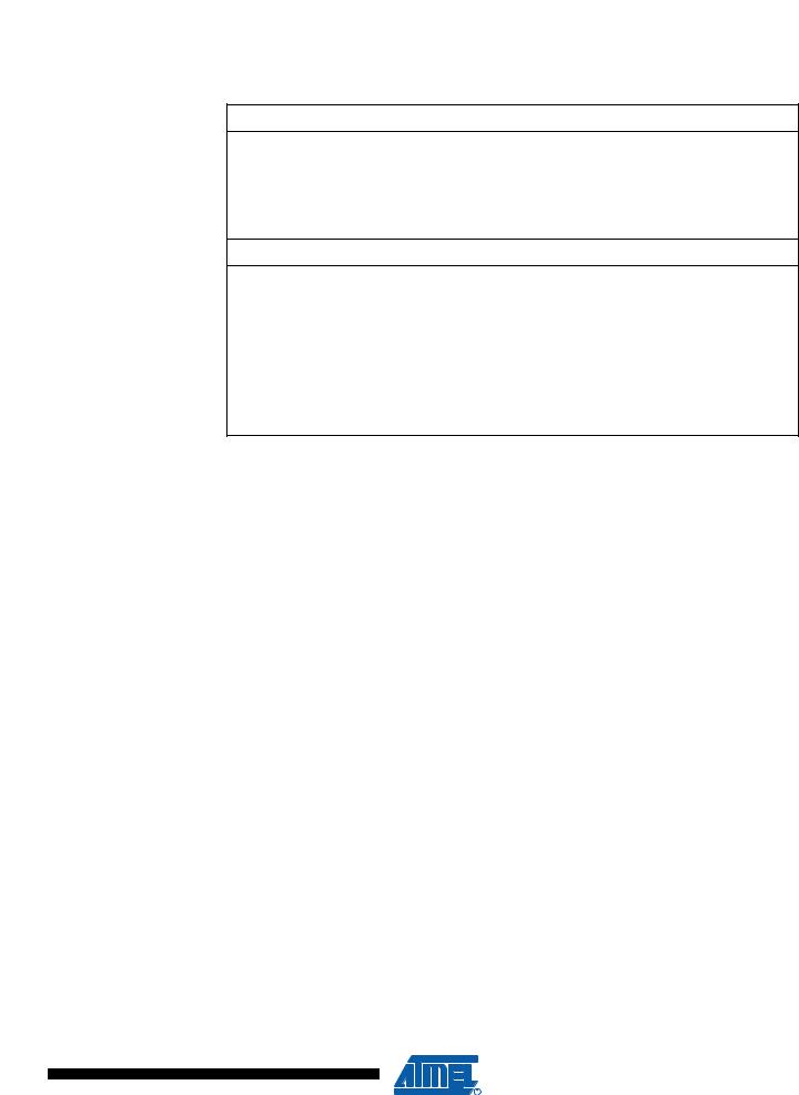
Assembly Code Example(1)
USART_ReadUCSRC:
; Read UCSRC
in r16,UBRRH
in r16,UCSRC
ret
C Code Example(1)
unsigned char USART_ReadUCSRC( void )
{
unsigned char ucsrc; /* Read UCSRC */ ucsrc = UBRRH; ucsrc = UCSRC; return ucsrc;
}
Note: 1. See “About Code Examples” on page 6.
The assembly code example returns the UCSRC value in r16.
Reading the UBRRH contents is not an atomic operation and therefore it can be read as an ordinary register, as long as the previous instruction did not access the register location.
19.10 Register Description
19.10.1UDR– USART I/O Data Register
Bit |
7 |
6 |
5 |
4 |
3 |
2 |
1 |
0 |
|
|
|
|
|
RXB[7:0] |
|
|
|
UDR (Read) |
|
|
|
|
|
TXB[7:0] |
|
|
|
UDR (Write) |
|
Read/Write |
R/W |
R/W |
R/W |
R/W |
R/W |
R/W |
R/W |
R/W |
|
Initial Value |
0 |
0 |
0 |
0 |
0 |
0 |
0 |
0 |
|
The USART Transmit Data Buffer Register and USART Receive Data Buffer Registers share the same I/O address referred to as USART Data Register or UDR. The Transmit Data Buffer Register (TXB) will be the destination for data written to the UDR Register location. Reading the UDR Register location will return the contents of the Receive Data Buffer Register (RXB).
For 5-, 6-, or 7-bit characters the upper unused bits will be ignored by the Transmitter and set to zero by the Receiver.
The transmit buffer can only be written when the UDRE Flag in the UCSRA Register is set. Data written to UDR when the UDRE Flag is not set, will be ignored by the USART Transmitter. When data is written to the transmit buffer, and the Transmitter is enabled, the Transmitter will load the data into the Transmit Shift Register when the Shift Register is empty. Then the data will be serially transmitted on the TxD pin.
The receive buffer consists of a two level FIFO. The FIFO will change its state whenever the receive buffer is accessed. Due to this behavior of the receive buffer, do not use Read-Modify- Write instructions (SBI and CBI) on this location. Be careful when using bit test instructions (SBIC and SBIS), since these also will change the state of the FIFO.
156
8159C–AVR–07/09

 ATmega8A
19.10.2UCSRA – USART Control and Status Register A
Bit |
7 |
6 |
5 |
4 |
3 |
2 |
1 |
0 |
|
|
RXC |
TXC |
UDRE |
FE |
DOR |
PE |
U2X |
MPCM |
UCSRA |
Read/Write |
R |
R/W |
R |
R |
R |
R |
R/W |
R/W |
|
Initial Value |
0 |
0 |
1 |
0 |
0 |
0 |
0 |
0 |
|
• Bit 7 – RXC: USART Receive Complete
This flag bit is set when there are unread data in the receive buffer and cleared when the receive buffer is empty (i.e. does not contain any unread data). If the Receiver is disabled, the receive buffer will be flushed and consequently the RXC bit will become zero. The RXC Flag can be used to generate a Receive Complete interrupt (see description of the RXCIE bit).
• Bit 6 – TXC: USART Transmit Complete
This flag bit is set when the entire frame in the Transmit Shift Register has been shifted out and there are no new data currently present in the transmit buffer (UDR). The TXC Flag bit is automatically cleared when a transmit complete interrupt is executed, or it can be cleared by writing a one to its bit location. The TXC Flag can generate a Transmit Complete interrupt (see description of the TXCIE bit).
• Bit 5 – UDRE: USART Data Register Empty
The UDRE Flag indicates if the transmit buffer (UDR) is ready to receive new data. If UDRE is one, the buffer is empty, and therefore ready to be written. The UDRE Flag can generate a Data Register Empty interrupt (see description of the UDRIE bit).
UDRE is set after a reset to indicate that the Transmitter is ready.
• Bit 4 – FE: Frame Error
This bit is set if the next character in the receive buffer had a Frame Error when received (i.e., when the first stop bit of the next character in the receive buffer is zero). This bit is valid until the receive buffer (UDR) is read. The FE bit is zero when the stop bit of received data is one. Always set this bit to zero when writing to UCSRA.
• Bit 3 – DOR: Data OverRun
This bit is set if a Data OverRun condition is detected. A Data OverRun occurs when the receive buffer is full (two characters), it is a new character waiting in the Receive Shift Register, and a new start bit is detected. This bit is valid until the receive buffer (UDR) is read. Always set this bit to zero when writing to UCSRA.
• Bit 2 – PE: Parity Error
This bit is set if the next character in the receive buffer had a Parity Error when received and the parity checking was enabled at that point (UPM1 = 1). This bit is valid until the receive buffer (UDR) is read. Always set this bit to zero when writing to UCSRA.
• Bit 1 – U2X: Double the USART transmission speed
This bit only has effect for the asynchronous operation. Write this bit to zero when using synchronous operation.
Writing this bit to one will reduce the divisor of the baud rate divider from 16 to 8 effectively doubling the transfer rate for asynchronous communication.
157
8159C–AVR–07/09

 ATmega8A
• Bit 0 – MPCM: Multi-processor Communication Mode
This bit enables the Multi-processor Communication mode. When the MPCM bit is written to one, all the incoming frames received by the USART Receiver that do not contain address information will be ignored. The Transmitter is unaffected by the MPCM setting. For more detailed information see “Multi-processor Communication Mode” on page 153.
19.10.3UCSRB – USART Control and Status Register B
Bit |
7 |
6 |
5 |
4 |
3 |
2 |
1 |
0 |
|
|
RXCIE |
TXCIE |
UDRIE |
RXEN |
TXEN |
UCSZ2 |
RXB8 |
TXB8 |
UCSRB |
Read/Write |
R/W |
R/W |
R/W |
R/W |
R/W |
R/W |
R |
R/W |
|
Initial Value |
0 |
0 |
0 |
0 |
0 |
0 |
0 |
0 |
|
• Bit 7 – RXCIE: RX Complete Interrupt Enable
Writing this bit to one enables interrupt on the RXC Flag. A USART Receive Complete interrupt will be generated only if the RXCIE bit is written to one, the Global Interrupt Flag in SREG is written to one and the RXC bit in UCSRA is set.
• Bit 6 – TXCIE: TX Complete Interrupt Enable
Writing this bit to one enables interrupt on the TXC Flag. A USART Transmit Complete interrupt will be generated only if the TXCIE bit is written to one, the Global Interrupt Flag in SREG is written to one and the TXC bit in UCSRA is set.
• Bit 5 – UDRIE: USART Data Register Empty Interrupt Enable
Writing this bit to one enables interrupt on the UDRE Flag. A Data Register Empty interrupt will be generated only if the UDRIE bit is written to one, the Global Interrupt Flag in SREG is written to one and the UDRE bit in UCSRA is set.
• Bit 4 – RXEN: Receiver Enable
Writing this bit to one enables the USART Receiver. The Receiver will override normal port operation for the RxD pin when enabled. Disabling the Receiver will flush the receive buffer invalidating the FE, DOR and PE Flags.
• Bit 3 – TXEN: Transmitter Enable
Writing this bit to one enables the USART Transmitter. The Transmitter will override normal port operation for the TxD pin when enabled. The disabling of the Transmitter (writing TXEN to zero) will not become effective until ongoing and pending transmissions are completed (i.e., when the Transmit Shift Register and Transmit Buffer Register do not contain data to be transmitted). When disabled, the Transmitter will no longer override the TxD port.
• Bit 2 – UCSZ2: Character Size
The UCSZ2 bits combined with the UCSZ1:0 bit in UCSRC sets the number of data bits (Character Size) in a frame the Receiver and Transmitter use.
• Bit 1 – RXB8: Receive Data Bit 8
RXB8 is the ninth data bit of the received character when operating with serial frames with nine data bits. Must be read before reading the low bits from UDR.
158
8159C–AVR–07/09

 ATmega8A
• Bit 0 – TXB8: Transmit Data Bit 8
TXB8 is the ninth data bit in the character to be transmitted when operating with serial frames with nine data bits. Must be written before writing the low bits to UDR.
19.10.4UCSRC – USART Control and Status Register C
Bit |
7 |
6 |
5 |
4 |
3 |
2 |
1 |
0 |
|
|
URSEL |
UMSEL |
UPM1 |
UPM0 |
USBS |
UCSZ1 |
UCSZ0 |
UCPOL |
UCSRC |
Read/Write |
R/W |
R/W |
R/W |
R/W |
R/W |
R/W |
R/W |
R/W |
|
Initial Value |
1 |
0 |
0 |
0 |
0 |
1 |
1 |
0 |
|
The UCSRC Register shares the same I/O location as the UBRRH Register. See the “Accessing UBRRH/UCSRC Registers” on page 154 section which describes how to access this register.
• Bit 7 – URSEL: Register Select
This bit selects between accessing the UCSRC or the UBRRH Register. It is read as one when reading UCSRC. The URSEL must be one when writing the UCSRC.
• Bit 6 – UMSEL: USART Mode Select
This bit selects between Asynchronous and Synchronous mode of operation.
Table 19-4. UMSEL Bit Settings
UMSEL |
Mode |
|
|
0 |
Asynchronous Operation |
|
|
1 |
Synchronous Operation |
|
|
• Bit 5:4 – UPM1:0: Parity Mode
These bits enable and set type of Parity Generation and Check. If enabled, the Transmitter will automatically generate and send the parity of the transmitted data bits within each frame. The Receiver will generate a parity value for the incoming data and compare it to the UPM0 setting. If a mismatch is detected, the PE Flag in UCSRA will be set.
Table 19-5. |
UPM Bits Settings |
|
|
UPM1 |
|
UPM0 |
Parity Mode |
|
|
|
|
0 |
|
0 |
Disabled |
|
|
|
|
0 |
|
1 |
Reserved |
|
|
|
|
1 |
|
0 |
Enabled, Even Parity |
|
|
|
|
1 |
|
1 |
Enabled, Odd Parity |
|
|
|
|
• Bit 3 – USBS: Stop Bit Select
This bit selects the number of stop bits to be inserted by the trAnsmitter. The Receiver ignores this setting.
Table 19-6. USBS Bit Settings
USBS |
Stop Bit(s) |
|
|
0 |
1-bit |
|
|
1 |
2-bit |
|
|
159
8159C–AVR–07/09