

Features
•High-performance, Low-power AVR® 8-bit Microcontroller
•Advanced RISC Architecture
–130 Powerful Instructions – Most Single-clock Cycle Execution
–32 x 8 General Purpose Working Registers
–Fully Static Operation
–Up to 16 MIPS Throughput at 16 MHz
–On-chip 2-cycle Multiplier
•High Endurance Non-volatile Memory segments
–8K Bytes of In-System Self-programmable Flash program memory
–512 Bytes EEPROM
–1K Byte Internal SRAM
–Write/Erase Cycles: 10,000 Flash/100,000 EEPROM
–Data retention: 20 years at 85°C/100 years at 25°C(1)
–Optional Boot Code Section with Independent Lock Bits
•In-System Programming by On-chip Boot Program
•True Read-While-Write Operation
–Programming Lock for Software Security
•Peripheral Features
–Two 8-bit Timer/Counters with Separate Prescaler, one Compare Mode
–One 16-bit Timer/Counter with Separate Prescaler, Compare Mode, and Capture Mode
–Real Time Counter with Separate Oscillator
–Three PWM Channels
–8-channel ADC in TQFP and QFN/MLF package
•Eight Channels 10-bit Accuracy
–6-channel ADC in PDIP package
•Six Channels 10-bit Accuracy
–Byte-oriented Two-wire Serial Interface
–Programmable Serial USART
–Master/Slave SPI Serial Interface
–Programmable Watchdog Timer with Separate On-chip Oscillator
–On-chip Analog Comparator
•Special Microcontroller Features
–Power-on Reset and Programmable Brown-out Detection
–Internal Calibrated RC Oscillator
–External and Internal Interrupt Sources
–Five Sleep Modes: Idle, ADC Noise Reduction, Power-save, Power-down, and Standby
•I/O and Packages
–23 Programmable I/O Lines
–28-lead PDIP, 32-lead TQFP, and 32-pad QFN/MLF
•Operating Voltages
–2.7 - 5.5V for ATmega8A
•Speed Grades
–0 - 16 MHz for ATmega8A
•Power Consumption at 4 Mhz, 3V, 25°C
–Active: 3.6 mA
–Idle Mode: 1.0 mA
–Power-down Mode: 0.5 µA
8-bit  with 8K Bytes In-System Programmable Flash
ATmega8A
8159C–AVR–07/09
ATmega8A
1. Pin Configurations
Figure 1-1. |
Pinout ATmega8A |
|
|
|
|
|
|
|
|
|
|
|
|
PDIP |
|
|
|
|
|
|
|
|
|
|
|
|
|
(RESET) PC6 |
|
|
1 |
28 |
|
|
PC5 (ADC5/SCL) |
|
(RXD) PD0 |
|
|
2 |
27 |
|
|
PC4 (ADC4/SDA) |
|
(TXD) PD1 |
|
3 |
26 |
|
|
PC3 (ADC3) |
|
|
(INT0) PD2 |
|
4 |
25 |
|
|
PC2 (ADC2) |
|
|
(INT1) PD3 |
|
5 |
24 |
|
|
PC1 (ADC1) |
|
|
(XCK/T0) PD4 |
|
6 |
23 |
|
|
PC0 (ADC0) |
|
|
VCC |
|
7 |
22 |
|
|
GND |
|
|
GND |
|
8 |
21 |
|
|
AREF |
|
|
(XTAL1/TOSC1) PB6 |
|
9 |
20 |
|
|
AVCC |
|
|
(XTAL2/TOSC2) PB7 |
|
10 |
19 |
|
|
PB5 (SCK) |
|
|
(T1) PD5 |
|
11 |
18 |
|
|
PB4 (MISO) |
|
|
(AIN0) PD6 |
|
12 |
17 |
|
|
PB3 (MOSI/OC2) |
|
|
(AIN1) PD7 |
|
13 |
16 |
|
|
PB2 (SS/OC1B) |
|
|
(ICP1) PB0 |
|
14 |
15 |
|
|
PB1 (OC1A) |
|
|
|
|
|
|
|
|
|
|
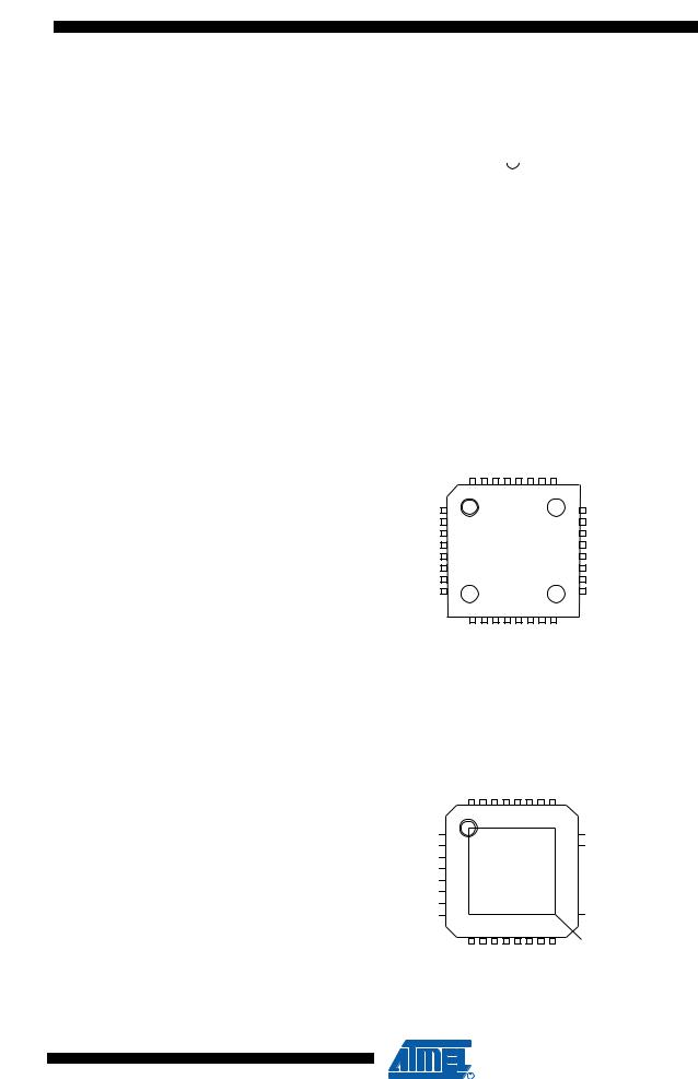
TQFP Top View
|
PD2 (INT0) |
PD1 (TXD) |
PD0 (RXD) |
|
PC6 (RESET) |
PC5 (ADC5/SCL) |
PC4 (ADC4/SDA) |
PC3 (ADC3) |
PC2 (ADC2) |
|
|
|
|
||||||||
|
|
|
||||||||
|
32 |
31 |
30 |
29 |
28 |
27 |
26 |
25 |
|
|
(INT1) PD3 |
1 |
|
|
|
|
|
|
|
24 |
PC1 (ADC1) |
(XCK/T0) PD4 |
2 |
|
|
|
|
|
|
|
23 |
PC0 (ADC0) |
GND |
3 |
|
|
|
|
|
|
|
22 |
ADC7 |
VCC |
4 |
|
|
|
|
|
|
|
21 |
GND |
GND |
5 |
|
|
|
|
|
|
|
20 |
AREF |
VCC |
6 |
|
|
|
|
|
|
|
19 |
ADC6 |
(XTAL1/TOSC1) PB6 |
7 |
|
|
|
|
|
|
|
18 |
AVCC |
(XTAL2/TOSC2) PB7 |
8 |
|
|
|
|
|
|
|
17 |
PB5 (SCK) |
|
9 |
10 |
11 |
12 |
13 |
14 |
15 |
16 |
|
|
|
(T1) PD5 |
(AIN0) PD6 |
(AIN1) PD7 |
|
(ICP1) PB0 |
(OC1A) PB1 |
(SS/OC1B) PB2 |
(MOSI/OC2) PB3 |
(MISO) PB4 |
|
(INT1) PD3  1 (XCK/T0) PD4
  2 GND
2 GND  3 VCC
3 VCC  4 GND
4 GND  5 VCC
5 VCC  6
6
(XTAL1/TOSC1) PB6 
 7 (XTAL2/TOSC2) PB7
 8
8
MLF Top View
PD2 (INT0) |
PD1 (TXD) |
PD0 (RXD) |
|
PC6 (RESET) |
PC5 (ADC5/SCL) |
PC4 (ADC4/SDA) |
PC3 (ADC3) |
PC2 (ADC2) |
|
||||||||
|
||||||||
32 |
31 |
30 |
29 |
28 |
27 |
26 |
25 |
|
9 |
10 |
11 |
12 |
13 |
14 |
15 |
16 |
(T1) PD5 |
(AIN0) PD6 |
(AIN1) PD7 |
(ICP1) PB0 |
(OC1A) PB1 |
(SS/OC1B) PB2 |
(MOSI/OC2) PB3 |
(MISO) PB4 |
24  PC1 (ADC1)
23 
 PC0 (ADC0)
22  ADC7
ADC7
21  GND
GND
20  AREF
AREF
19  ADC6
ADC6
18  AVCC
AVCC
17 
 PB5 (SCK)
NOTE:
The large center pad underneath the MLF packages is made of metal and internally connected to GND. It should be soldered or glued to the PCB to ensure good mechanical stability. If the center pad is left unconneted, the package might loosen from the PCB.
2
8159C–AVR–07/09