

- •Features
- •1. Pin Configurations
- •1.1 Pin Descriptions
- •1.1.3 Port B (PB7:0) XTAL1/XTAL2/TOSC1/TOSC2
- •1.1.4 Port C (PC5:0)
- •1.1.5 PC6/RESET
- •1.1.6 Port D (PD7:0)
- •1.1.8 AREF
- •1.1.9 ADC7:6 (TQFP and QFN/MLF Package Only)
- •2. Overview
- •2.1 Block Diagram
- •2.2 Comparison Between ATmega48PA and ATmega88PA
- •3. Resources
- •4. Data Retention
- •5. About Code Examples
- •6. AVR CPU Core
- •6.1 Overview
- •6.2 ALU – Arithmetic Logic Unit
- •6.3 Status Register
- •6.3.1 SREG – AVR Status Register
- •6.4 General Purpose Register File
- •6.5 Stack Pointer
- •6.5.1 SPH and SPL – Stack Pointer High and Stack Pointer Low Register
- •6.6 Instruction Execution Timing
- •6.7 Reset and Interrupt Handling
- •6.7.1 Interrupt Response Time
- •7. AVR Memories
- •7.1 Overview
- •7.3 SRAM Data Memory
- •7.3.1 Data Memory Access Times
- •7.4 EEPROM Data Memory
- •7.4.1 EEPROM Read/Write Access
- •7.4.2 Preventing EEPROM Corruption
- •7.5 I/O Memory
- •7.5.1 General Purpose I/O Registers
- •7.6 Register Description
- •7.6.1 EEARH and EEARL – The EEPROM Address Register
- •7.6.2 EEDR – The EEPROM Data Register
- •7.6.3 EECR – The EEPROM Control Register
- •7.6.4 GPIOR2 – General Purpose I/O Register 2
- •7.6.5 GPIOR1 – General Purpose I/O Register 1
- •7.6.6 GPIOR0 – General Purpose I/O Register 0
- •8. System Clock and Clock Options
- •8.1 Clock Systems and their Distribution
- •8.2 Clock Sources
- •8.2.1 Default Clock Source
- •8.2.2 Clock Startup Sequence
- •8.3 Low Power Crystal Oscillator
- •8.4 Full Swing Crystal Oscillator
- •8.5 Low Frequency Crystal Oscillator
- •8.6 Calibrated Internal RC Oscillator
- •8.7 128 kHz Internal Oscillator
- •8.8 External Clock
- •8.9 Clock Output Buffer
- •8.10 Timer/Counter Oscillator
- •8.11 System Clock Prescaler
- •8.12 Register Description
- •8.12.1 OSCCAL – Oscillator Calibration Register
- •8.12.2 CLKPR – Clock Prescale Register
- •9. Power Management and Sleep Modes
- •9.1 Sleep Modes
- •9.2 BOD Disable
- •9.3 Idle Mode
- •9.4 ADC Noise Reduction Mode
- •9.7 Standby Mode
- •9.8 Extended Standby Mode
- •9.9 Power Reduction Register
- •9.10 Minimizing Power Consumption
- •9.10.1 Analog to Digital Converter
- •9.10.2 Analog Comparator
- •9.10.4 Internal Voltage Reference
- •9.10.5 Watchdog Timer
- •9.10.6 Port Pins
- •9.11 Register Description
- •9.11.1 SMCR – Sleep Mode Control Register
- •9.11.2 MCUCR – MCU Control Register
- •9.11.3 PRR – Power Reduction Register
- •10. System Control and Reset
- •10.1 Resetting the AVR
- •10.2 Reset Sources
- •10.3 Power-on Reset
- •10.4 External Reset
- •10.6 Watchdog System Reset
- •10.7 Internal Voltage Reference
- •10.8 Watchdog Timer
- •10.8.1 Features
- •10.8.2 Overview
- •10.9 Register Description
- •10.9.1 MCUSR – MCU Status Register
- •10.9.2 WDTCSR – Watchdog Timer Control Register
- •11. Interrupts
- •11.1 Interrupt Vectors in ATmega48PA
- •11.2 Interrupt Vectors in ATmega88PA
- •11.3 Register Description
- •11.3.1 Moving Interrupts Between Application and Boot Space, ATmega88PA
- •11.3.2 MCUCR – MCU Control Register
- •12. External Interrupts
- •12.1 Pin Change Interrupt Timing
- •12.2 Register Description
- •12.2.1 EICRA – External Interrupt Control Register A
- •12.2.2 EIMSK – External Interrupt Mask Register
- •12.2.3 EIFR – External Interrupt Flag Register
- •12.2.4 PCICR – Pin Change Interrupt Control Register
- •12.2.5 PCIFR – Pin Change Interrupt Flag Register
- •12.2.6 PCMSK2 – Pin Change Mask Register 2
- •12.2.7 PCMSK1 – Pin Change Mask Register 1
- •12.2.8 PCMSK0 – Pin Change Mask Register 0
- •13. I/O-Ports
- •13.1 Overview
- •13.2 Ports as General Digital I/O
- •13.2.1 Configuring the Pin
- •13.2.2 Toggling the Pin
- •13.2.3 Switching Between Input and Output
- •13.2.4 Reading the Pin Value
- •13.2.5 Digital Input Enable and Sleep Modes
- •13.2.6 Unconnected Pins
- •13.3 Alternate Port Functions
- •13.3.1 Alternate Functions of Port B
- •13.3.2 Alternate Functions of Port C
- •13.3.3 Alternate Functions of Port D
- •13.4 Register Description
- •13.4.1 MCUCR – MCU Control Register
- •13.4.2 PORTB – The Port B Data Register
- •13.4.3 DDRB – The Port B Data Direction Register
- •13.4.4 PINB – The Port B Input Pins Address
- •13.4.5 PORTC – The Port C Data Register
- •13.4.6 DDRC – The Port C Data Direction Register
- •13.4.7 PINC – The Port C Input Pins Address
- •13.4.8 PORTD – The Port D Data Register
- •13.4.9 DDRD – The Port D Data Direction Register
- •13.4.10 PIND – The Port D Input Pins Address
- •14. 8-bit Timer/Counter0 with PWM
- •14.1 Features
- •14.2 Overview
- •14.2.1 Definitions
- •14.2.2 Registers
- •14.3 Timer/Counter Clock Sources
- •14.4 Counter Unit
- •14.5 Output Compare Unit
- •14.5.1 Force Output Compare
- •14.5.2 Compare Match Blocking by TCNT0 Write
- •14.5.3 Using the Output Compare Unit
- •14.6 Compare Match Output Unit
- •14.6.1 Compare Output Mode and Waveform Generation
- •14.7 Modes of Operation
- •14.7.1 Normal Mode
- •14.7.2 Clear Timer on Compare Match (CTC) Mode
- •14.7.3 Fast PWM Mode
- •14.7.4 Phase Correct PWM Mode
- •14.8 Timer/Counter Timing Diagrams
- •14.9 Register Description
- •14.9.1 TCCR0A – Timer/Counter Control Register A
- •14.9.2 TCCR0B – Timer/Counter Control Register B
- •14.9.3 TCNT0 – Timer/Counter Register
- •14.9.4 OCR0A – Output Compare Register A
- •14.9.5 OCR0B – Output Compare Register B
- •14.9.6 TIMSK0 – Timer/Counter Interrupt Mask Register
- •14.9.7 TIFR0 – Timer/Counter 0 Interrupt Flag Register
- •15. 16-bit Timer/Counter1 with PWM
- •15.1 Features
- •15.2 Overview
- •15.2.1 Registers
- •15.2.2 Definitions
- •15.3.1 Reusing the Temporary High Byte Register
- •15.4 Timer/Counter Clock Sources
- •15.5 Counter Unit
- •15.6 Input Capture Unit
- •15.6.1 Input Capture Trigger Source
- •15.6.2 Noise Canceler
- •15.6.3 Using the Input Capture Unit
- •15.7 Output Compare Units
- •15.7.1 Force Output Compare
- •15.7.2 Compare Match Blocking by TCNT1 Write
- •15.7.3 Using the Output Compare Unit
- •15.8 Compare Match Output Unit
- •15.8.1 Compare Output Mode and Waveform Generation
- •15.9 Modes of Operation
- •15.9.1 Normal Mode
- •15.9.2 Clear Timer on Compare Match (CTC) Mode
- •15.9.3 Fast PWM Mode
- •15.9.4 Phase Correct PWM Mode
- •15.9.5 Phase and Frequency Correct PWM Mode
- •15.10 Timer/Counter Timing Diagrams
- •15.11 Register Description
- •15.11.1 TCCR1A – Timer/Counter1 Control Register A
- •15.11.2 TCCR1B – Timer/Counter1 Control Register B
- •15.11.3 TCCR1C – Timer/Counter1 Control Register C
- •15.11.4 TCNT1H and TCNT1L – Timer/Counter1
- •15.11.5 OCR1AH and OCR1AL – Output Compare Register 1 A
- •15.11.6 OCR1BH and OCR1BL – Output Compare Register 1 B
- •15.11.7 ICR1H and ICR1L – Input Capture Register 1
- •15.11.8 TIMSK1 – Timer/Counter1 Interrupt Mask Register
- •15.11.9 TIFR1 – Timer/Counter1 Interrupt Flag Register
- •16. Timer/Counter0 and Timer/Counter1 Prescalers
- •16.1 Internal Clock Source
- •16.2 Prescaler Reset
- •16.3 External Clock Source
- •16.4 Register Description
- •16.4.1 GTCCR – General Timer/Counter Control Register
- •17. 8-bit Timer/Counter2 with PWM and Asynchronous Operation
- •17.1 Features
- •17.2 Overview
- •17.2.1 Registers
- •17.2.2 Definitions
- •17.3 Timer/Counter Clock Sources
- •17.4 Counter Unit
- •17.5 Output Compare Unit
- •17.5.1 Force Output Compare
- •17.5.2 Compare Match Blocking by TCNT2 Write
- •17.5.3 Using the Output Compare Unit
- •17.6 Compare Match Output Unit
- •17.6.1 Compare Output Mode and Waveform Generation
- •17.7 Modes of Operation
- •17.7.1 Normal Mode
- •17.7.2 Clear Timer on Compare Match (CTC) Mode
- •17.7.3 Fast PWM Mode
- •17.7.4 Phase Correct PWM Mode
- •17.8 Timer/Counter Timing Diagrams
- •17.9 Asynchronous Operation of Timer/Counter2
- •17.10 Timer/Counter Prescaler
- •17.11 Register Description
- •17.11.1 TCCR2A – Timer/Counter Control Register A
- •17.11.2 TCCR2B – Timer/Counter Control Register B
- •17.11.3 TCNT2 – Timer/Counter Register
- •17.11.4 OCR2A – Output Compare Register A
- •17.11.5 OCR2B – Output Compare Register B
- •17.11.6 TIMSK2 – Timer/Counter2 Interrupt Mask Register
- •17.11.7 TIFR2 – Timer/Counter2 Interrupt Flag Register
- •17.11.8 ASSR – Asynchronous Status Register
- •17.11.9 GTCCR – General Timer/Counter Control Register
- •18. SPI – Serial Peripheral Interface
- •18.1 Features
- •18.2 Overview
- •18.3 SS Pin Functionality
- •18.3.1 Slave Mode
- •18.3.2 Master Mode
- •18.4 Data Modes
- •18.5 Register Description
- •18.5.1 SPCR – SPI Control Register
- •18.5.2 SPSR – SPI Status Register
- •18.5.3 SPDR – SPI Data Register
- •19. USART0
- •19.1 Features
- •19.2 Overview
- •19.3 Clock Generation
- •19.3.1 Internal Clock Generation – The Baud Rate Generator
- •19.3.2 Double Speed Operation (U2Xn)
- •19.3.3 External Clock
- •19.3.4 Synchronous Clock Operation
- •19.4 Frame Formats
- •19.4.1 Parity Bit Calculation
- •19.5 USART Initialization
- •19.6 Data Transmission – The USART Transmitter
- •19.6.1 Sending Frames with 5 to 8 Data Bit
- •19.6.2 Sending Frames with 9 Data Bit
- •19.6.3 Transmitter Flags and Interrupts
- •19.6.4 Parity Generator
- •19.6.5 Disabling the Transmitter
- •19.7 Data Reception – The USART Receiver
- •19.7.1 Receiving Frames with 5 to 8 Data Bits
- •19.7.2 Receiving Frames with 9 Data Bits
- •19.7.3 Receive Compete Flag and Interrupt
- •19.7.4 Receiver Error Flags
- •19.7.5 Parity Checker
- •19.7.6 Disabling the Receiver
- •19.7.7 Flushing the Receive Buffer
- •19.8 Asynchronous Data Reception
- •19.8.1 Asynchronous Clock Recovery
- •19.8.2 Asynchronous Data Recovery
- •19.8.3 Asynchronous Operational Range
- •19.9.1 Using MPCMn
- •19.10 Register Description
- •19.10.1 UDRn – USART I/O Data Register n
- •19.10.2 UCSRnA – USART Control and Status Register n A
- •19.10.3 UCSRnB – USART Control and Status Register n B
- •19.10.4 UCSRnC – USART Control and Status Register n C
- •19.10.5 UBRRnL and UBRRnH – USART Baud Rate Registers
- •19.11 Examples of Baud Rate Setting
- •20. USART in SPI Mode
- •20.1 Features
- •20.2 Overview
- •20.3 Clock Generation
- •20.4 SPI Data Modes and Timing
- •20.5 Frame Formats
- •20.5.1 USART MSPIM Initialization
- •20.6 Data Transfer
- •20.6.1 Transmitter and Receiver Flags and Interrupts
- •20.6.2 Disabling the Transmitter or Receiver
- •20.7 AVR USART MSPIM vs. AVR SPI
- •20.8 Register Description
- •20.8.1 UDRn – USART MSPIM I/O Data Register
- •20.8.2 UCSRnA – USART MSPIM Control and Status Register n A
- •20.8.3 UCSRnB – USART MSPIM Control and Status Register n B
- •20.8.4 UCSRnC – USART MSPIM Control and Status Register n C
- •20.8.5 USART MSPIM Baud Rate Registers - UBRRnL and UBRRnH
- •21. 2-wire Serial Interface
- •21.1 Features
- •21.2.1 TWI Terminology
- •21.2.2 Electrical Interconnection
- •21.3 Data Transfer and Frame Format
- •21.3.1 Transferring Bits
- •21.3.2 START and STOP Conditions
- •21.3.3 Address Packet Format
- •21.3.4 Data Packet Format
- •21.3.5 Combining Address and Data Packets into a Transmission
- •21.5 Overview of the TWI Module
- •21.5.1 SCL and SDA Pins
- •21.5.2 Bit Rate Generator Unit
- •21.5.3 Bus Interface Unit
- •21.5.4 Address Match Unit
- •21.5.5 Control Unit
- •21.6 Using the TWI
- •21.7 Transmission Modes
- •21.7.1 Master Transmitter Mode
- •21.7.2 Master Receiver Mode
- •21.7.3 Slave Receiver Mode
- •21.7.4 Slave Transmitter Mode
- •21.7.5 Miscellaneous States
- •21.7.6 Combining Several TWI Modes
- •21.9 Register Description
- •21.9.1 TWBR – TWI Bit Rate Register
- •21.9.2 TWCR – TWI Control Register
- •21.9.3 TWSR – TWI Status Register
- •21.9.4 TWDR – TWI Data Register
- •21.9.5 TWAR – TWI (Slave) Address Register
- •21.9.6 TWAMR – TWI (Slave) Address Mask Register
- •22. Analog Comparator
- •22.1 Overview
- •22.2 Analog Comparator Multiplexed Input
- •22.3 Register Description
- •22.3.1 ADCSRB – ADC Control and Status Register B
- •22.3.2 ACSR – Analog Comparator Control and Status Register
- •22.3.3 DIDR1 – Digital Input Disable Register 1
- •23. Analog-to-Digital Converter
- •23.1 Features
- •23.2 Overview
- •23.3 Starting a Conversion
- •23.4 Prescaling and Conversion Timing
- •23.5 Changing Channel or Reference Selection
- •23.5.1 ADC Input Channels
- •23.5.2 ADC Voltage Reference
- •23.6 ADC Noise Canceler
- •23.6.1 Analog Input Circuitry
- •23.6.2 Analog Noise Canceling Techniques
- •23.6.3 ADC Accuracy Definitions
- •23.7 ADC Conversion Result
- •23.8 Temperature Measurement
- •23.9 Register Description
- •23.9.1 ADMUX – ADC Multiplexer Selection Register
- •23.9.2 ADCSRA – ADC Control and Status Register A
- •23.9.3 ADCL and ADCH – The ADC Data Register
- •23.9.3.1 ADLAR = 0
- •23.9.3.2 ADLAR = 1
- •23.9.4 ADCSRB – ADC Control and Status Register B
- •23.9.5 DIDR0 – Digital Input Disable Register 0
- •24. debugWIRE On-chip Debug System
- •24.1 Features
- •24.2 Overview
- •24.3 Physical Interface
- •24.4 Software Break Points
- •24.5 Limitations of debugWIRE
- •24.6 Register Description
- •24.6.1 DWDR – debugWire Data Register
- •25. Self-Programming the Flash, ATmega48PA
- •25.1 Overview
- •25.1.1 Performing Page Erase by SPM
- •25.1.2 Filling the Temporary Buffer (Page Loading)
- •25.1.3 Performing a Page Write
- •25.2.1 EEPROM Write Prevents Writing to SPMCSR
- •25.2.2 Reading the Fuse and Lock Bits from Software
- •25.2.3 Preventing Flash Corruption
- •25.2.4 Programming Time for Flash when Using SPM
- •25.2.5 Simple Assembly Code Example for a Boot Loader
- •25.3 Register Description’
- •25.3.1 SPMCSR – Store Program Memory Control and Status Register
- •26.1 Features
- •26.2 Overview
- •26.3 Application and Boot Loader Flash Sections
- •26.3.1 Application Section
- •26.3.2 BLS – Boot Loader Section
- •26.5 Boot Loader Lock Bits
- •26.6 Entering the Boot Loader Program
- •26.8.1 Performing Page Erase by SPM
- •26.8.2 Filling the Temporary Buffer (Page Loading)
- •26.8.3 Performing a Page Write
- •26.8.4 Using the SPM Interrupt
- •26.8.5 Consideration While Updating BLS
- •26.8.7 Setting the Boot Loader Lock Bits by SPM
- •26.8.8 EEPROM Write Prevents Writing to SPMCSR
- •26.8.9 Reading the Fuse and Lock Bits from Software
- •26.8.10 Reading the Signature Row from Software
- •26.8.11 Preventing Flash Corruption
- •26.8.12 Programming Time for Flash when Using SPM
- •26.8.13 Simple Assembly Code Example for a Boot Loader
- •26.8.14 ATmega88PA Boot Loader Parameters
- •26.9 Register Description
- •26.9.1 SPMCSR – Store Program Memory Control and Status Register
- •27. Memory Programming
- •27.1 Program And Data Memory Lock Bits
- •27.2 Fuse Bits
- •27.2.1 Latching of Fuses
- •27.3 Signature Bytes
- •27.4 Calibration Byte
- •27.5 Page Size
- •27.6 Parallel Programming Parameters, Pin Mapping, and Commands
- •27.6.1 Signal Names
- •27.7 Parallel Programming
- •27.7.1 Enter Programming Mode
- •27.7.2 Considerations for Efficient Programming
- •27.7.3 Chip Erase
- •27.7.4 Programming the Flash
- •27.7.5 Programming the EEPROM
- •27.7.6 Reading the Flash
- •27.7.7 Reading the EEPROM
- •27.7.8 Programming the Fuse Low Bits
- •27.7.9 Programming the Fuse High Bits
- •27.7.10 Programming the Extended Fuse Bits
- •27.7.11 Programming the Lock Bits
- •27.7.12 Reading the Fuse and Lock Bits
- •27.7.13 Reading the Signature Bytes
- •27.7.14 Reading the Calibration Byte
- •27.7.15 Parallel Programming Characteristics
- •27.8 Serial Downloading
- •27.8.1 Serial Programming Pin Mapping
- •27.8.2 Serial Programming Algorithm
- •27.8.3 Serial Programming Instruction set
- •27.8.4 SPI Serial Programming Characteristics
- •28. Electrical Characteristics
- •28.1 Absolute Maximum Ratings*
- •28.2 DC Characteristics
- •28.2.1 ATmega48PA DC Characteristics
- •28.2.2 ATmega88PA DC Characteristics
- •28.3 Speed Grades
- •28.4 Clock Characteristics
- •28.4.1 Calibrated Internal RC Oscillator Accuracy
- •28.4.2 External Clock Drive Waveforms
- •28.4.3 External Clock Drive
- •28.5 System and Reset Characteristics
- •28.6 SPI Timing Characteristics
- •28.8 ADC Characteristics
- •28.9 Parallel Programming Characteristics
- •29. Typical Characteristics
- •29.1 ATmega48PA
- •29.1.1 Active Supply Current
- •29.1.2 Idle Supply Current
- •Example
- •29.1.6 Standby Supply Current
- •29.1.8 Pin Driver Strength
- •29.1.9 Pin Threshold and Hysteresis
- •29.1.10 BOD Threshold
- •29.1.11 Internal Oscilllator Speed
- •29.1.12 Current Consumption of Peripheral Units
- •29.1.13 Current Consumption in Reset and Reset Pulsewidth
- •29.2 ATmega88PA
- •29.2.1 Active Supply Current
- •29.2.2 Idle Supply Current
- •Example
- •29.2.6 Standby Supply Current
- •29.2.8 Pin Driver Strength
- •29.2.9 Pin Threshold and Hysteresis
- •29.2.10 BOD Threshold
- •29.2.11 Internal Oscilllator Speed
- •29.2.12 Current Consumption of Peripheral Units
- •29.2.13 Current Consumption in Reset and Reset Pulsewidth
- •30. Register Summary
- •31. Instruction Set Summary
- •32. Ordering Information
- •32.1 ATmega48PA
- •32.2 ATmega88PA
- •33. Packaging Information
- •34. Errata
- •34.1 Errata ATmega48PA
- •34.2 Errata ATmega88PA
- •35. Datasheet Revision History
- •Table of Contents

 ATmega48PA/88PA
21.7Transmission Modes
The TWI can operate in one of four major modes. These are named Master Transmitter (MT), Master Receiver (MR), Slave Transmitter (ST) and Slave Receiver (SR). Several of these modes can be used in the same application. As an example, the TWI can use MT mode to write data into a TWI EEPROM, MR mode to read the data back from the EEPROM. If other masters are present in the system, some of these might transmit data to the TWI, and then SR mode would be used. It is the application software that decides which modes are legal.
The following sections describe each of these modes. Possible status codes are described along with figures detailing data transmission in each of the modes. These figures contain the following abbreviations:
S: START condition
Rs: REPEATED START condition
R: Read bit (high level at SDA)
W: Write bit (low level at SDA)
A: Acknowledge bit (low level at SDA)
A: Not acknowledge bit (high level at SDA)
Data: 8-bit data byte
P: STOP condition
SLA: Slave Address
In Figure 21-12 to Figure 21-18, circles are used to indicate that the TWINT Flag is set. The numbers in the circles show the status code held in TWSR, with the prescaler bits masked to zero. At these points, actions must be taken by the application to continue or complete the TWI transfer. The TWI transfer is suspended until the TWINT Flag is cleared by software.
When the TWINT Flag is set, the status code in TWSR is used to determine the appropriate software action. For each status code, the required software action and details of the following serial transfer are given in Table 21-2 to Table 21-5. Note that the prescaler bits are masked to zero in these tables.
21.7.1Master Transmitter Mode
In the Master Transmitter mode, a number of data bytes are transmitted to a Slave Receiver (see Figure 21-11). In order to enter a Master mode, a START condition must be transmitted. The format of the following address packet determines whether Master Transmitter or Master Receiver mode is to be entered. If SLA+W is transmitted, MT mode is entered, if SLA+R is transmitted, MR mode is entered. All the status codes mentioned in this section assume that the prescaler bits are zero or are masked to zero.
222
8161B–AVR–01/09
ATmega48PA/88PA
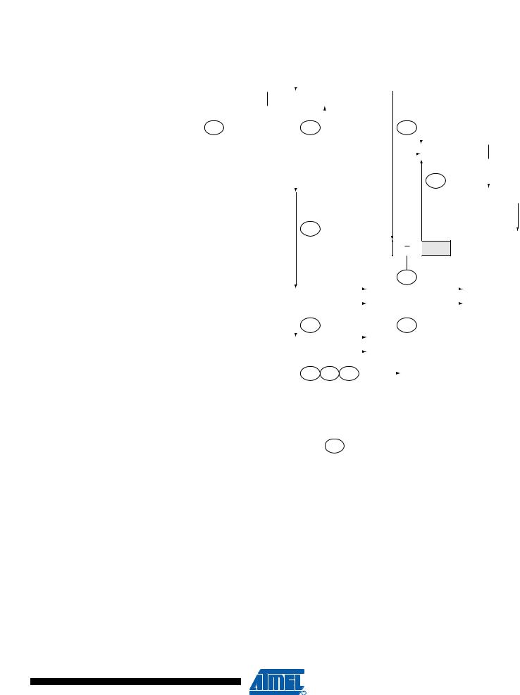
Figure 21-11. Data Transfer in Master Transmitter Mode
|
|
|
|
|
|
|
VCC |
|
|
|
|
|
|
|
|
|
|
|
|
|
|
|
|
|
|
|
|
|
|
|
|
|
|
|
|
|
|
|
|
|
|
|
|
|
|
|
|
Device 1 |
|
Device 2 |
|
Device 3 |
........ |
|
|
|
|
|
|
|
|
|
|
|
|
Device n |
|
|
R1 |
|
R2 |
|
|||||||
|
MASTER |
|
SLAVE |
|
|
|
|
|
|||||||
TRANSMITTER |
|
RECEIVER |
|
|
|
|
|
|
|
|
|
|
|
|
|
|
|
|
|
|
|
|
|
|
|
|
|
|
|
|
|
|
|
|
|
|
|
|
|
|
|
|
|
|
|
|
|
|
|
|
|
|
|
|
|
|
|
|
|
|
|
|
|
SDA
SCL
A START condition is sent by writing the following value to TWCR:
TWCR |
TWINT |
TWEA |
TWSTA |
TWSTO |
TWWC |
TWEN |
– |
TWIE |
value |
1 |
X |
1 |
0 |
X |
1 |
0 |
X |
|
|
|
|
|
|
|
|
|
TWEN must be set to enable the 2-wire Serial Interface, TWSTA must be written to one to transmit a START condition and TWINT must be written to one to clear the TWINT Flag. The TWI will then test the 2-wire Serial Bus and generate a START condition as soon as the bus becomes free. After a START condition has been transmitted, the TWINT Flag is set by hardware, and the status code in TWSR will be 0x08 (see Table 21-2). In order to enter MT mode, SLA+W must be transmitted. This is done by writing SLA+W to TWDR. Thereafter the TWINT bit should be cleared (by writing it to one) to continue the transfer. This is accomplished by writing the following value to TWCR:
TWCR |
TWINT |
TWEA |
TWSTA |
TWSTO |
TWWC |
TWEN |
– |
TWIE |
value |
1 |
X |
0 |
0 |
X |
1 |
0 |
X |
|
|
|
|
|
|
|
|
|
When SLA+W have been transmitted and an acknowledgement bit has been received, TWINT is set again and a number of status codes in TWSR are possible. Possible status codes in Master mode are 0x18, 0x20, or 0x38. The appropriate action to be taken for each of these status codes is detailed in Table 21-2.
When SLA+W has been successfully transmitted, a data packet should be transmitted. This is done by writing the data byte to TWDR. TWDR must only be written when TWINT is high. If not, the access will be discarded, and the Write Collision bit (TWWC) will be set in the TWCR Register. After updating TWDR, the TWINT bit should be cleared (by writing it to one) to continue the transfer. This is accomplished by writing the following value to TWCR:
TWCR |
TWINT |
TWEA |
TWSTA |
TWSTO |
TWWC |
TWEN |
– |
TWIE |
value |
1 |
X |
0 |
0 |
X |
1 |
0 |
X |
|
|
|
|
|
|
|
|
|
This scheme is repeated until the last byte has been sent and the transfer is ended by generating a STOP condition or a repeated START condition. A STOP condition is generated by writing the following value to TWCR:
TWCR |
TWINT |
TWEA |
TWSTA |
TWSTO |
TWWC |
TWEN |
– |
TWIE |
value |
1 |
X |
0 |
1 |
X |
1 |
0 |
X |
|
|
|
|
|
|
|
|
|
A REPEATED START condition is generated by writing the following value to TWCR:
TWCR |
TWINT |
TWEA |
TWSTA |
TWSTO |
TWWC |
TWEN |
– |
TWIE |
value |
1 |
X |
1 |
0 |
X |
1 |
0 |
X |
|
|
|
|
|
|
|
|
|
223
8161B–AVR–01/09

 ATmega48PA/88PA
After a repeated START condition (state 0x10) the 2-wire Serial Interface can access the same Slave again, or a new Slave without transmitting a STOP condition. Repeated START enables the Master to switch between Slaves, Master Transmitter mode and Master Receiver mode without losing control of the bus.
Table 21-2. |
Status codes for Master Transmitter Mode |
|
|
|
|
||
Status Code |
|
Application Software Response |
|
|
|||
(TWSR) |
Status of the 2-wire Serial Bus |
To/from TWDR |
|
To TWCR |
|
|
|
Prescaler Bits |
and 2-wire Serial Interface |
|
|
|
|||
are 0 |
Hardware |
|
STA |
STO |
TWIN |
TWE |
Next Action Taken by TWI Hardware |
|
|
|
|
|
T |
A |
|
0x08 |
A START condition has been |
Load SLA+W |
0 |
0 |
1 |
X |
SLA+W will be transmitted; |
|
transmitted |
|
|
|
|
|
ACK or NOT ACK will be received |
0x10 |
A repeated START condition |
Load SLA+W or |
0 |
0 |
1 |
X |
SLA+W will be transmitted; |
|
has been transmitted |
Load SLA+R |
0 |
0 |
1 |
X |
ACK or NOT ACK will be received |
|
|
SLA+R will be transmitted; |
|||||
|
|
|
|
|
|
|
Logic will switch to Master Receiver mode |
0x18 |
SLA+W has been transmitted; |
Load data byte or |
0 |
0 |
1 |
X |
Data byte will be transmitted and ACK or NOT ACK will |
|
ACK has been received |
|
|
|
|
|
be received |
|
|
No TWDR action or |
1 |
0 |
1 |
X |
Repeated START will be transmitted |
|
|
No TWDR action or |
0 |
1 |
1 |
X |
STOP condition will be transmitted and |
|
|
|
|
|
1 |
X |
TWSTO Flag will be reset |
|
|
No TWDR action |
1 |
1 |
STOP condition followed by a START condition will be |
||
|
|
|
|
|
|
|
transmitted and TWSTO Flag will be reset |
0x20 |
SLA+W has been transmitted; |
Load data byte or |
0 |
0 |
1 |
X |
Data byte will be transmitted and ACK or NOT ACK will |
|
NOT ACK has been received |
No TWDR action or |
1 |
0 |
1 |
X |
be received |
|
|
Repeated START will be transmitted |
|||||
|
|
No TWDR action or |
0 |
1 |
1 |
X |
STOP condition will be transmitted and |
|
|
No TWDR action |
1 |
1 |
1 |
X |
TWSTO Flag will be reset |
|
|
STOP condition followed by a START condition will be |
|||||
|
|
|
|
|
|
|
transmitted and TWSTO Flag will be reset |
0x28 |
Data byte has been transmit- |
Load data byte or |
0 |
0 |
1 |
X |
Data byte will be transmitted and ACK or NOT ACK will |
|
ted; |
|
|
|
1 |
X |
be received |
|
ACK has been received |
No TWDR action or |
1 |
0 |
Repeated START will be transmitted |
||
|
|
No TWDR action or |
0 |
1 |
1 |
X |
STOP condition will be transmitted and |
|
|
|
|
1 |
1 |
X |
TWSTO Flag will be reset |
|
|
No TWDR action |
1 |
STOP condition followed by a START condition will be |
|||
|
|
|
|
|
|
|
transmitted and TWSTO Flag will be reset |
0x30 |
Data byte has been transmit- |
Load data byte or |
0 |
0 |
1 |
X |
Data byte will be transmitted and ACK or NOT ACK will |
|
ted; |
|
|
|
|
|
be received |
|
NOT ACK has been received |
No TWDR action or |
1 |
0 |
1 |
X |
Repeated START will be transmitted |
|
|
No TWDR action or |
0 |
1 |
1 |
X |
STOP condition will be transmitted and |
|
|
No TWDR action |
1 |
1 |
1 |
X |
TWSTO Flag will be reset |
|
|
STOP condition followed by a START condition will be |
|||||
|
|
|
|
|
|
|
transmitted and TWSTO Flag will be reset |
0x38 |
Arbitration lost in SLA+W or |
No TWDR action or |
0 |
0 |
1 |
X |
2-wire Serial Bus will be released and not addressed |
|
data bytes |
|
|
|
|
|
Slave mode entered |
|
|
No TWDR action |
1 |
0 |
1 |
X |
A START condition will be transmitted when the bus |
|
|
|
|
|
|
|
becomes free |
224
8161B–AVR–01/09
 ATmega48PA/88PA
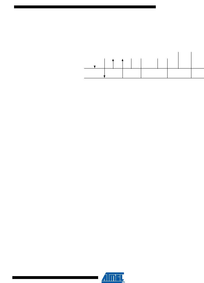
Figure 21-12. Formats and States in the Master Transmitter Mode
MT
Successfull |
|
|
|
|
|
|
|
|
|
|
|
|
|
|
|
|
|
|
|
|
|
|
|
|
|
|
|
|
|
|
|
|
|
|
|
|
|
|
|
|
|
|
|
|
|
|
|
|
|
|
|
|
|
|
|
|
|
S |
SLA |
W |
|
A |
DATA |
A |
P |
|
|
||||||||
transmission |
|
|
|
|
||||||||||||||
to a slave |
|
|
|
|
|
|
|
|
|
|
|
|
|
|
|
|
|
|
receiver |
|
|
|
|
|
|
|
|
|
|
|
|
|
|
|
|
|
|
|
|
|
|
|
|
|
|
|
|
|
|
|
|
|
|
|
|
|
|
|
$08 |
|
|
$18 |
|
|
$28 |
|
|
|
|
|
|||||
Next transfer |
|
|
|
|
|
|
|
|
|
|
|
|
|
|
|
|
|
|
|
|
|
|
|
|
|
|
|
|
|
|
|
|
|
|
|
||
|
|
|
|
|
|
|
|
|
|
|
|
|
RS |
SLA |
W |
|||
started with a |
|
|
|
|
|
|
|
|
|
|
|
|
|
|||||
|
|
|
|
|
|
|
|
|
|
|
|
|
||||||
repeated start |
|
|
|
|
|
|
|
|
|
|
|
|
|
|
|
|
|
|
condition |
|
|
|
|
|
|
|
|
|
|
|
|
|
|
|
|
|
|
|
|
|
|
|
|
|
|
|
|
|
|
|
|
|
|
|
|
|
|
|
|
|
|
|
|
|
|
|
|
|
|
|
|
$10 |
|
|
|
|
|
|
|
|
|
|
|
|
|
|
|
|
|
|
|
|
|
|
Not acknowledge |
|
|
|
|
|
|
|
|
|
|
|
|
|
|
|
|
R |
|
|
|
|
|
|
|
|
|
P |
|
|
|
|
|
|
|
|||
received after the |
|
|
|
|
|
A |
|
|
|
|
|
|
|
|
|
|||
|
|
|
|
|
|
|
|
|
|
|
|
|
|
|||||
slave address |
|
|
|
|
|
|
|
|
|
|
|
|
|
|
|
|
|
|
|
|
|
|
|
|
|
|
|
|
|
|
|
|
|
|
|
|
|
$20
MR
Not acknowledge
received after a data A P byte
|
|
|
|
|
|
|
|
$30 |
|
|
|
||||
Arbitration lost in slave |
|
|
|
|
|
|
|
|
|
|
|
|
|
|
|
|
|
|
|
Other master |
|
|
|
|
|
|
Other master |
|
|||
address or data byte |
A or A |
|
continues |
|
|
A or A |
continues |
|
|||||||
|
|
|
|
|
|
|
|
|
|
|
|
|
|
|
|
|
|
|
|
|
|
|
|
|
|
|
|
|
|
|
|
|
$38 |
|
|
|
|
$38 |
|
|
|
||||||
Arbitration lost and |
|
|
|
|
|
|
|
|
|
|
|
|
|
|
|
|
|
|
|
|
|
|
|
|
|
|
|
|
|
||
A |
|
Other master |
|
|
|
|
|
|
|
|
|||||
addressed as slave |
|
continues |
|
|
|
|
|
|
|
|
|||||
|
|
|
|
|
|
|
|
|
|
To corresponding |
|
||||
|
|
|
|
|
|
|
|
|
|
|
|||||
|
$68 |
$78 |
$B0 |
|
|
|
|
||||||||
|
|
|
|
states in slave mode |
|
||||||||||
|
|
|
|
|
|
|
|
|
|
|
|
|
|
|
|
|
From master to slave |
DATA |
A |
Any number of data bytes |
|
and their associated acknowledge bits |
|||
|
From slave to master |
n |
|
This number (contained in TWSR) corresponds |
|
|
|||
|
|
|
to a defined state of the 2-Wire Serial Bus. The |
|
|
|
|
||
|
|
|
|
prescaler bits are zero or masked to zero |
21.7.2Master Receiver Mode
In the Master Receiver mode, a number of data bytes are received from a Slave Transmitter (Slave see Figure 21-13). In order to enter a Master mode, a START condition must be transmitted. The format of the following address packet determines whether Master Transmitter or Master Receiver mode is to be entered. If SLA+W is transmitted, MT mode is entered, if SLA+R is transmitted, MR mode is entered. All the status codes mentioned in this section assume that the prescaler bits are zero or are masked to zero.
225
8161B–AVR–01/09
 ATmega48PA/88PA
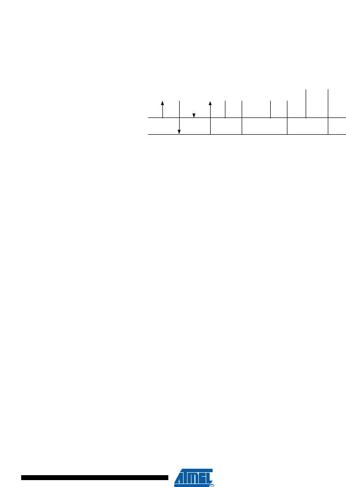
Figure 21-13. Data Transfer in Master Receiver Mode
|
|
|
|
|
|
|
VCC |
|
|
|
|
|
|
|
|
|
|
|
|
|
|
|
|
|
|
|
|
|
|
|
|
|
|
|
|
|
|
|
|
|
|
|
|
|
|
|
|
Device 1 |
|
Device 2 |
|
Device 3 |
........ |
|
|
|
|
|
|
|
|
|
|
|
|
Device n |
|
|
R1 |
|
R2 |
|
|||||||
MASTER |
|
|
SLAVE |
|
|
|
|
|
|||||||
RECEIVER |
|
TRANSMITTER |
|
|
|
|
|
|
|
|
|
|
|
|
|
|
|
|
|
|
|
|
|
|
|
|
|
|
|
|
|
|
|
|
|
|
|
|
|
|
|
|
|
|
|
|
|
|
|
|
|
|
|
|
|
|
|
|
|
|
|
|
|
SDA
SCL
A START condition is sent by writing the following value to TWCR:
TWCR |
TWINT |
TWEA |
TWSTA |
TWSTO |
TWWC |
TWEN |
– |
TWIE |
value |
1 |
X |
1 |
0 |
X |
1 |
0 |
X |
|
|
|
|
|
|
|
|
|
TWEN must be written to one to enable the 2-wire Serial Interface, TWSTA must be written to one to transmit a START condition and TWINT must be set to clear the TWINT Flag. The TWI will then test the 2-wire Serial Bus and generate a START condition as soon as the bus becomes free. After a START condition has been transmitted, the TWINT Flag is set by hardware, and the status code in TWSR will be 0x08 (See Table 21-2). In order to enter MR mode, SLA+R must be transmitted. This is done by writing SLA+R to TWDR. Thereafter the TWINT bit should be cleared (by writing it to one) to continue the transfer. This is accomplished by writing the following value to TWCR:
TWCR |
TWINT |
TWEA |
TWSTA |
TWSTO |
TWWC |
TWEN |
– |
TWIE |
value |
1 |
X |
0 |
0 |
X |
1 |
0 |
X |
|
|
|
|
|
|
|
|
|
When SLA+R have been transmitted and an acknowledgement bit has been received, TWINT is set again and a number of status codes in TWSR are possible. Possible status codes in Master mode are 0x38, 0x40, or 0x48. The appropriate action to be taken for each of these status codes is detailed in Table 21-3. Received data can be read from the TWDR Register when the TWINT Flag is set high by hardware. This scheme is repeated until the last byte has been received. After the last byte has been received, the MR should inform the ST by sending a NACK after the last received data byte. The transfer is ended by generating a STOP condition or a repeated START condition. A STOP condition is generated by writing the following value to TWCR:
TWCR |
TWINT |
TWEA |
TWSTA |
TWSTO |
TWWC |
TWEN |
– |
TWIE |
value |
1 |
X |
0 |
1 |
X |
1 |
0 |
X |
|
|
|
|
|
|
|
|
|
A REPEATED START condition is generated by writing the following value to TWCR:
TWCR |
TWINT |
TWEA |
TWSTA |
TWSTO |
TWWC |
TWEN |
– |
TWIE |
value |
1 |
X |
1 |
0 |
X |
1 |
0 |
X |
|
|
|
|
|
|
|
|
|
After a repeated START condition (state 0x10) the 2-wire Serial Interface can access the same Slave again, or a new Slave without transmitting a STOP condition. Repeated START enables
226
8161B–AVR–01/09

 ATmega48PA/88PA
the Master to switch between Slaves, Master Transmitter mode and Master Receiver mode without losing control over the bus.
Table 21-3. |
Status codes for Master Receiver Mode |
|
|
|
|
|
||
Status Code |
|
Application Software Response |
|
|
||||
(TWSR) |
Status of the 2-wire Serial Bus |
|
|
|
To TWCR |
|
|
|
Prescaler Bits |
and 2-wire Serial Interface |
To/from TWDR |
|
|
|
|
||
are 0 |
Hardware |
|
STA |
STO |
TWIN |
TWE |
Next Action Taken by TWI Hardware |
|
|
|
|||||||
|
|
|
|
|
|
T |
A |
|
0x08 |
A START condition has been |
Load SLA+R |
|
0 |
0 |
1 |
X |
SLA+R will be transmitted |
|
transmitted |
|
|
|
|
|
|
ACK or NOT ACK will be received |
0x10 |
A repeated START condition |
Load SLA+R or |
|
0 |
0 |
1 |
X |
SLA+R will be transmitted |
|
has been transmitted |
|
|
|
|
|
|
ACK or NOT ACK will be received |
|
|
Load SLA+W |
|
0 |
0 |
1 |
X |
SLA+W will be transmitted |
|
|
|
|
|
|
|
|
Logic will switch to Master Transmitter mode |
0x38 |
Arbitration lost in SLA+R or |
No TWDR action or |
|
0 |
0 |
1 |
X |
2-wire Serial Bus will be released and not addressed |
|
NOT ACK bit |
No TWDR action |
|
1 |
0 |
1 |
X |
Slave mode will be entered |
|
|
|
A START condition will be transmitted when the bus |
|||||
|
|
|
|
|
|
|
|
becomes free |
0x40 |
SLA+R has been transmitted; |
No TWDR action or |
|
0 |
0 |
1 |
0 |
Data byte will be received and NOT ACK will be |
|
ACK has been received |
No TWDR action |
|
0 |
0 |
1 |
1 |
returned |
|
|
|
Data byte will be received and ACK will be returned |
|||||
|
|
|
|
|
|
|
|
|
0x48 |
SLA+R has been transmitted; |
No TWDR action or |
|
1 |
0 |
1 |
X |
Repeated START will be transmitted |
|
NOT ACK has been received |
No TWDR action or |
|
0 |
1 |
1 |
X |
STOP condition will be transmitted and TWSTO Flag |
|
|
No TWDR action |
|
1 |
1 |
1 |
X |
will be reset |
|
|
|
STOP condition followed by a START condition will be |
|||||
|
|
|
|
|
|
|
|
transmitted and TWSTO Flag will be reset |
0x50 |
Data byte has been received; |
Read data byte or |
|
0 |
0 |
1 |
0 |
Data byte will be received and NOT ACK will be |
|
ACK has been returned |
Read data byte |
|
0 |
0 |
1 |
1 |
returned |
|
|
|
Data byte will be received and ACK will be returned |
|||||
0x58 |
Data byte has been received; |
Read data byte or |
|
1 |
0 |
1 |
X |
Repeated START will be transmitted |
|
NOT ACK has been returned |
Read data byte or |
|
0 |
1 |
1 |
X |
STOP condition will be transmitted and TWSTO Flag |
|
|
Read data byte |
|
1 |
1 |
1 |
X |
will be reset |
|
|
|
STOP condition followed by a START condition will be |
|||||
|
|
|
|
|
|
|
|
transmitted and TWSTO Flag will be reset |
227
8161B–AVR–01/09