
- •Features
- •1. Pin Configurations
- •1.1 Pin Descriptions
- •1.1.3 Port B (PB7:0) XTAL1/XTAL2/TOSC1/TOSC2
- •1.1.4 Port C (PC5:0)
- •1.1.5 PC6/RESET
- •1.1.6 Port D (PD7:0)
- •1.1.8 AREF
- •1.1.9 ADC7:6 (TQFP and QFN/MLF Package Only)
- •2. Overview
- •2.1 Block Diagram
- •2.2 Comparison Between ATmega48PA and ATmega88PA
- •3. Resources
- •4. Data Retention
- •5. About Code Examples
- •6. AVR CPU Core
- •6.1 Overview
- •6.2 ALU – Arithmetic Logic Unit
- •6.3 Status Register
- •6.3.1 SREG – AVR Status Register
- •6.4 General Purpose Register File
- •6.5 Stack Pointer
- •6.5.1 SPH and SPL – Stack Pointer High and Stack Pointer Low Register
- •6.6 Instruction Execution Timing
- •6.7 Reset and Interrupt Handling
- •6.7.1 Interrupt Response Time
- •7. AVR Memories
- •7.1 Overview
- •7.3 SRAM Data Memory
- •7.3.1 Data Memory Access Times
- •7.4 EEPROM Data Memory
- •7.4.1 EEPROM Read/Write Access
- •7.4.2 Preventing EEPROM Corruption
- •7.5 I/O Memory
- •7.5.1 General Purpose I/O Registers
- •7.6 Register Description
- •7.6.1 EEARH and EEARL – The EEPROM Address Register
- •7.6.2 EEDR – The EEPROM Data Register
- •7.6.3 EECR – The EEPROM Control Register
- •7.6.4 GPIOR2 – General Purpose I/O Register 2
- •7.6.5 GPIOR1 – General Purpose I/O Register 1
- •7.6.6 GPIOR0 – General Purpose I/O Register 0
- •8. System Clock and Clock Options
- •8.1 Clock Systems and their Distribution
- •8.2 Clock Sources
- •8.2.1 Default Clock Source
- •8.2.2 Clock Startup Sequence
- •8.3 Low Power Crystal Oscillator
- •8.4 Full Swing Crystal Oscillator
- •8.5 Low Frequency Crystal Oscillator
- •8.6 Calibrated Internal RC Oscillator
- •8.7 128 kHz Internal Oscillator
- •8.8 External Clock
- •8.9 Clock Output Buffer
- •8.10 Timer/Counter Oscillator
- •8.11 System Clock Prescaler
- •8.12 Register Description
- •8.12.1 OSCCAL – Oscillator Calibration Register
- •8.12.2 CLKPR – Clock Prescale Register
- •9. Power Management and Sleep Modes
- •9.1 Sleep Modes
- •9.2 BOD Disable
- •9.3 Idle Mode
- •9.4 ADC Noise Reduction Mode
- •9.7 Standby Mode
- •9.8 Extended Standby Mode
- •9.9 Power Reduction Register
- •9.10 Minimizing Power Consumption
- •9.10.1 Analog to Digital Converter
- •9.10.2 Analog Comparator
- •9.10.4 Internal Voltage Reference
- •9.10.5 Watchdog Timer
- •9.10.6 Port Pins
- •9.11 Register Description
- •9.11.1 SMCR – Sleep Mode Control Register
- •9.11.2 MCUCR – MCU Control Register
- •9.11.3 PRR – Power Reduction Register
- •10. System Control and Reset
- •10.1 Resetting the AVR
- •10.2 Reset Sources
- •10.3 Power-on Reset
- •10.4 External Reset
- •10.6 Watchdog System Reset
- •10.7 Internal Voltage Reference
- •10.8 Watchdog Timer
- •10.8.1 Features
- •10.8.2 Overview
- •10.9 Register Description
- •10.9.1 MCUSR – MCU Status Register
- •10.9.2 WDTCSR – Watchdog Timer Control Register
- •11. Interrupts
- •11.1 Interrupt Vectors in ATmega48PA
- •11.2 Interrupt Vectors in ATmega88PA
- •11.3 Register Description
- •11.3.1 Moving Interrupts Between Application and Boot Space, ATmega88PA
- •11.3.2 MCUCR – MCU Control Register
- •12. External Interrupts
- •12.1 Pin Change Interrupt Timing
- •12.2 Register Description
- •12.2.1 EICRA – External Interrupt Control Register A
- •12.2.2 EIMSK – External Interrupt Mask Register
- •12.2.3 EIFR – External Interrupt Flag Register
- •12.2.4 PCICR – Pin Change Interrupt Control Register
- •12.2.5 PCIFR – Pin Change Interrupt Flag Register
- •12.2.6 PCMSK2 – Pin Change Mask Register 2
- •12.2.7 PCMSK1 – Pin Change Mask Register 1
- •12.2.8 PCMSK0 – Pin Change Mask Register 0
- •13. I/O-Ports
- •13.1 Overview
- •13.2 Ports as General Digital I/O
- •13.2.1 Configuring the Pin
- •13.2.2 Toggling the Pin
- •13.2.3 Switching Between Input and Output
- •13.2.4 Reading the Pin Value
- •13.2.5 Digital Input Enable and Sleep Modes
- •13.2.6 Unconnected Pins
- •13.3 Alternate Port Functions
- •13.3.1 Alternate Functions of Port B
- •13.3.2 Alternate Functions of Port C
- •13.3.3 Alternate Functions of Port D
- •13.4 Register Description
- •13.4.1 MCUCR – MCU Control Register
- •13.4.2 PORTB – The Port B Data Register
- •13.4.3 DDRB – The Port B Data Direction Register
- •13.4.4 PINB – The Port B Input Pins Address
- •13.4.5 PORTC – The Port C Data Register
- •13.4.6 DDRC – The Port C Data Direction Register
- •13.4.7 PINC – The Port C Input Pins Address
- •13.4.8 PORTD – The Port D Data Register
- •13.4.9 DDRD – The Port D Data Direction Register
- •13.4.10 PIND – The Port D Input Pins Address
- •14. 8-bit Timer/Counter0 with PWM
- •14.1 Features
- •14.2 Overview
- •14.2.1 Definitions
- •14.2.2 Registers
- •14.3 Timer/Counter Clock Sources
- •14.4 Counter Unit
- •14.5 Output Compare Unit
- •14.5.1 Force Output Compare
- •14.5.2 Compare Match Blocking by TCNT0 Write
- •14.5.3 Using the Output Compare Unit
- •14.6 Compare Match Output Unit
- •14.6.1 Compare Output Mode and Waveform Generation
- •14.7 Modes of Operation
- •14.7.1 Normal Mode
- •14.7.2 Clear Timer on Compare Match (CTC) Mode
- •14.7.3 Fast PWM Mode
- •14.7.4 Phase Correct PWM Mode
- •14.8 Timer/Counter Timing Diagrams
- •14.9 Register Description
- •14.9.1 TCCR0A – Timer/Counter Control Register A
- •14.9.2 TCCR0B – Timer/Counter Control Register B
- •14.9.3 TCNT0 – Timer/Counter Register
- •14.9.4 OCR0A – Output Compare Register A
- •14.9.5 OCR0B – Output Compare Register B
- •14.9.6 TIMSK0 – Timer/Counter Interrupt Mask Register
- •14.9.7 TIFR0 – Timer/Counter 0 Interrupt Flag Register
- •15. 16-bit Timer/Counter1 with PWM
- •15.1 Features
- •15.2 Overview
- •15.2.1 Registers
- •15.2.2 Definitions
- •15.3.1 Reusing the Temporary High Byte Register
- •15.4 Timer/Counter Clock Sources
- •15.5 Counter Unit
- •15.6 Input Capture Unit
- •15.6.1 Input Capture Trigger Source
- •15.6.2 Noise Canceler
- •15.6.3 Using the Input Capture Unit
- •15.7 Output Compare Units
- •15.7.1 Force Output Compare
- •15.7.2 Compare Match Blocking by TCNT1 Write
- •15.7.3 Using the Output Compare Unit
- •15.8 Compare Match Output Unit
- •15.8.1 Compare Output Mode and Waveform Generation
- •15.9 Modes of Operation
- •15.9.1 Normal Mode
- •15.9.2 Clear Timer on Compare Match (CTC) Mode
- •15.9.3 Fast PWM Mode
- •15.9.4 Phase Correct PWM Mode
- •15.9.5 Phase and Frequency Correct PWM Mode
- •15.10 Timer/Counter Timing Diagrams
- •15.11 Register Description
- •15.11.1 TCCR1A – Timer/Counter1 Control Register A
- •15.11.2 TCCR1B – Timer/Counter1 Control Register B
- •15.11.3 TCCR1C – Timer/Counter1 Control Register C
- •15.11.4 TCNT1H and TCNT1L – Timer/Counter1
- •15.11.5 OCR1AH and OCR1AL – Output Compare Register 1 A
- •15.11.6 OCR1BH and OCR1BL – Output Compare Register 1 B
- •15.11.7 ICR1H and ICR1L – Input Capture Register 1
- •15.11.8 TIMSK1 – Timer/Counter1 Interrupt Mask Register
- •15.11.9 TIFR1 – Timer/Counter1 Interrupt Flag Register
- •16. Timer/Counter0 and Timer/Counter1 Prescalers
- •16.1 Internal Clock Source
- •16.2 Prescaler Reset
- •16.3 External Clock Source
- •16.4 Register Description
- •16.4.1 GTCCR – General Timer/Counter Control Register
- •17. 8-bit Timer/Counter2 with PWM and Asynchronous Operation
- •17.1 Features
- •17.2 Overview
- •17.2.1 Registers
- •17.2.2 Definitions
- •17.3 Timer/Counter Clock Sources
- •17.4 Counter Unit
- •17.5 Output Compare Unit
- •17.5.1 Force Output Compare
- •17.5.2 Compare Match Blocking by TCNT2 Write
- •17.5.3 Using the Output Compare Unit
- •17.6 Compare Match Output Unit
- •17.6.1 Compare Output Mode and Waveform Generation
- •17.7 Modes of Operation
- •17.7.1 Normal Mode
- •17.7.2 Clear Timer on Compare Match (CTC) Mode
- •17.7.3 Fast PWM Mode
- •17.7.4 Phase Correct PWM Mode
- •17.8 Timer/Counter Timing Diagrams
- •17.9 Asynchronous Operation of Timer/Counter2
- •17.10 Timer/Counter Prescaler
- •17.11 Register Description
- •17.11.1 TCCR2A – Timer/Counter Control Register A
- •17.11.2 TCCR2B – Timer/Counter Control Register B
- •17.11.3 TCNT2 – Timer/Counter Register
- •17.11.4 OCR2A – Output Compare Register A
- •17.11.5 OCR2B – Output Compare Register B
- •17.11.6 TIMSK2 – Timer/Counter2 Interrupt Mask Register
- •17.11.7 TIFR2 – Timer/Counter2 Interrupt Flag Register
- •17.11.8 ASSR – Asynchronous Status Register
- •17.11.9 GTCCR – General Timer/Counter Control Register
- •18. SPI – Serial Peripheral Interface
- •18.1 Features
- •18.2 Overview
- •18.3 SS Pin Functionality
- •18.3.1 Slave Mode
- •18.3.2 Master Mode
- •18.4 Data Modes
- •18.5 Register Description
- •18.5.1 SPCR – SPI Control Register
- •18.5.2 SPSR – SPI Status Register
- •18.5.3 SPDR – SPI Data Register
- •19. USART0
- •19.1 Features
- •19.2 Overview
- •19.3 Clock Generation
- •19.3.1 Internal Clock Generation – The Baud Rate Generator
- •19.3.2 Double Speed Operation (U2Xn)
- •19.3.3 External Clock
- •19.3.4 Synchronous Clock Operation
- •19.4 Frame Formats
- •19.4.1 Parity Bit Calculation
- •19.5 USART Initialization
- •19.6 Data Transmission – The USART Transmitter
- •19.6.1 Sending Frames with 5 to 8 Data Bit
- •19.6.2 Sending Frames with 9 Data Bit
- •19.6.3 Transmitter Flags and Interrupts
- •19.6.4 Parity Generator
- •19.6.5 Disabling the Transmitter
- •19.7 Data Reception – The USART Receiver
- •19.7.1 Receiving Frames with 5 to 8 Data Bits
- •19.7.2 Receiving Frames with 9 Data Bits
- •19.7.3 Receive Compete Flag and Interrupt
- •19.7.4 Receiver Error Flags
- •19.7.5 Parity Checker
- •19.7.6 Disabling the Receiver
- •19.7.7 Flushing the Receive Buffer
- •19.8 Asynchronous Data Reception
- •19.8.1 Asynchronous Clock Recovery
- •19.8.2 Asynchronous Data Recovery
- •19.8.3 Asynchronous Operational Range
- •19.9.1 Using MPCMn
- •19.10 Register Description
- •19.10.1 UDRn – USART I/O Data Register n
- •19.10.2 UCSRnA – USART Control and Status Register n A
- •19.10.3 UCSRnB – USART Control and Status Register n B
- •19.10.4 UCSRnC – USART Control and Status Register n C
- •19.10.5 UBRRnL and UBRRnH – USART Baud Rate Registers
- •19.11 Examples of Baud Rate Setting
- •20. USART in SPI Mode
- •20.1 Features
- •20.2 Overview
- •20.3 Clock Generation
- •20.4 SPI Data Modes and Timing
- •20.5 Frame Formats
- •20.5.1 USART MSPIM Initialization
- •20.6 Data Transfer
- •20.6.1 Transmitter and Receiver Flags and Interrupts
- •20.6.2 Disabling the Transmitter or Receiver
- •20.7 AVR USART MSPIM vs. AVR SPI
- •20.8 Register Description
- •20.8.1 UDRn – USART MSPIM I/O Data Register
- •20.8.2 UCSRnA – USART MSPIM Control and Status Register n A
- •20.8.3 UCSRnB – USART MSPIM Control and Status Register n B
- •20.8.4 UCSRnC – USART MSPIM Control and Status Register n C
- •20.8.5 USART MSPIM Baud Rate Registers - UBRRnL and UBRRnH
- •21. 2-wire Serial Interface
- •21.1 Features
- •21.2.1 TWI Terminology
- •21.2.2 Electrical Interconnection
- •21.3 Data Transfer and Frame Format
- •21.3.1 Transferring Bits
- •21.3.2 START and STOP Conditions
- •21.3.3 Address Packet Format
- •21.3.4 Data Packet Format
- •21.3.5 Combining Address and Data Packets into a Transmission
- •21.5 Overview of the TWI Module
- •21.5.1 SCL and SDA Pins
- •21.5.2 Bit Rate Generator Unit
- •21.5.3 Bus Interface Unit
- •21.5.4 Address Match Unit
- •21.5.5 Control Unit
- •21.6 Using the TWI
- •21.7 Transmission Modes
- •21.7.1 Master Transmitter Mode
- •21.7.2 Master Receiver Mode
- •21.7.3 Slave Receiver Mode
- •21.7.4 Slave Transmitter Mode
- •21.7.5 Miscellaneous States
- •21.7.6 Combining Several TWI Modes
- •21.9 Register Description
- •21.9.1 TWBR – TWI Bit Rate Register
- •21.9.2 TWCR – TWI Control Register
- •21.9.3 TWSR – TWI Status Register
- •21.9.4 TWDR – TWI Data Register
- •21.9.5 TWAR – TWI (Slave) Address Register
- •21.9.6 TWAMR – TWI (Slave) Address Mask Register
- •22. Analog Comparator
- •22.1 Overview
- •22.2 Analog Comparator Multiplexed Input
- •22.3 Register Description
- •22.3.1 ADCSRB – ADC Control and Status Register B
- •22.3.2 ACSR – Analog Comparator Control and Status Register
- •22.3.3 DIDR1 – Digital Input Disable Register 1
- •23. Analog-to-Digital Converter
- •23.1 Features
- •23.2 Overview
- •23.3 Starting a Conversion
- •23.4 Prescaling and Conversion Timing
- •23.5 Changing Channel or Reference Selection
- •23.5.1 ADC Input Channels
- •23.5.2 ADC Voltage Reference
- •23.6 ADC Noise Canceler
- •23.6.1 Analog Input Circuitry
- •23.6.2 Analog Noise Canceling Techniques
- •23.6.3 ADC Accuracy Definitions
- •23.7 ADC Conversion Result
- •23.8 Temperature Measurement
- •23.9 Register Description
- •23.9.1 ADMUX – ADC Multiplexer Selection Register
- •23.9.2 ADCSRA – ADC Control and Status Register A
- •23.9.3 ADCL and ADCH – The ADC Data Register
- •23.9.3.1 ADLAR = 0
- •23.9.3.2 ADLAR = 1
- •23.9.4 ADCSRB – ADC Control and Status Register B
- •23.9.5 DIDR0 – Digital Input Disable Register 0
- •24. debugWIRE On-chip Debug System
- •24.1 Features
- •24.2 Overview
- •24.3 Physical Interface
- •24.4 Software Break Points
- •24.5 Limitations of debugWIRE
- •24.6 Register Description
- •24.6.1 DWDR – debugWire Data Register
- •25. Self-Programming the Flash, ATmega48PA
- •25.1 Overview
- •25.1.1 Performing Page Erase by SPM
- •25.1.2 Filling the Temporary Buffer (Page Loading)
- •25.1.3 Performing a Page Write
- •25.2.1 EEPROM Write Prevents Writing to SPMCSR
- •25.2.2 Reading the Fuse and Lock Bits from Software
- •25.2.3 Preventing Flash Corruption
- •25.2.4 Programming Time for Flash when Using SPM
- •25.2.5 Simple Assembly Code Example for a Boot Loader
- •25.3 Register Description’
- •25.3.1 SPMCSR – Store Program Memory Control and Status Register
- •26.1 Features
- •26.2 Overview
- •26.3 Application and Boot Loader Flash Sections
- •26.3.1 Application Section
- •26.3.2 BLS – Boot Loader Section
- •26.5 Boot Loader Lock Bits
- •26.6 Entering the Boot Loader Program
- •26.8.1 Performing Page Erase by SPM
- •26.8.2 Filling the Temporary Buffer (Page Loading)
- •26.8.3 Performing a Page Write
- •26.8.4 Using the SPM Interrupt
- •26.8.5 Consideration While Updating BLS
- •26.8.7 Setting the Boot Loader Lock Bits by SPM
- •26.8.8 EEPROM Write Prevents Writing to SPMCSR
- •26.8.9 Reading the Fuse and Lock Bits from Software
- •26.8.10 Reading the Signature Row from Software
- •26.8.11 Preventing Flash Corruption
- •26.8.12 Programming Time for Flash when Using SPM
- •26.8.13 Simple Assembly Code Example for a Boot Loader
- •26.8.14 ATmega88PA Boot Loader Parameters
- •26.9 Register Description
- •26.9.1 SPMCSR – Store Program Memory Control and Status Register
- •27. Memory Programming
- •27.1 Program And Data Memory Lock Bits
- •27.2 Fuse Bits
- •27.2.1 Latching of Fuses
- •27.3 Signature Bytes
- •27.4 Calibration Byte
- •27.5 Page Size
- •27.6 Parallel Programming Parameters, Pin Mapping, and Commands
- •27.6.1 Signal Names
- •27.7 Parallel Programming
- •27.7.1 Enter Programming Mode
- •27.7.2 Considerations for Efficient Programming
- •27.7.3 Chip Erase
- •27.7.4 Programming the Flash
- •27.7.5 Programming the EEPROM
- •27.7.6 Reading the Flash
- •27.7.7 Reading the EEPROM
- •27.7.8 Programming the Fuse Low Bits
- •27.7.9 Programming the Fuse High Bits
- •27.7.10 Programming the Extended Fuse Bits
- •27.7.11 Programming the Lock Bits
- •27.7.12 Reading the Fuse and Lock Bits
- •27.7.13 Reading the Signature Bytes
- •27.7.14 Reading the Calibration Byte
- •27.7.15 Parallel Programming Characteristics
- •27.8 Serial Downloading
- •27.8.1 Serial Programming Pin Mapping
- •27.8.2 Serial Programming Algorithm
- •27.8.3 Serial Programming Instruction set
- •27.8.4 SPI Serial Programming Characteristics
- •28. Electrical Characteristics
- •28.1 Absolute Maximum Ratings*
- •28.2 DC Characteristics
- •28.2.1 ATmega48PA DC Characteristics
- •28.2.2 ATmega88PA DC Characteristics
- •28.3 Speed Grades
- •28.4 Clock Characteristics
- •28.4.1 Calibrated Internal RC Oscillator Accuracy
- •28.4.2 External Clock Drive Waveforms
- •28.4.3 External Clock Drive
- •28.5 System and Reset Characteristics
- •28.6 SPI Timing Characteristics
- •28.8 ADC Characteristics
- •28.9 Parallel Programming Characteristics
- •29. Typical Characteristics
- •29.1 ATmega48PA
- •29.1.1 Active Supply Current
- •29.1.2 Idle Supply Current
- •Example
- •29.1.6 Standby Supply Current
- •29.1.8 Pin Driver Strength
- •29.1.9 Pin Threshold and Hysteresis
- •29.1.10 BOD Threshold
- •29.1.11 Internal Oscilllator Speed
- •29.1.12 Current Consumption of Peripheral Units
- •29.1.13 Current Consumption in Reset and Reset Pulsewidth
- •29.2 ATmega88PA
- •29.2.1 Active Supply Current
- •29.2.2 Idle Supply Current
- •Example
- •29.2.6 Standby Supply Current
- •29.2.8 Pin Driver Strength
- •29.2.9 Pin Threshold and Hysteresis
- •29.2.10 BOD Threshold
- •29.2.11 Internal Oscilllator Speed
- •29.2.12 Current Consumption of Peripheral Units
- •29.2.13 Current Consumption in Reset and Reset Pulsewidth
- •30. Register Summary
- •31. Instruction Set Summary
- •32. Ordering Information
- •32.1 ATmega48PA
- •32.2 ATmega88PA
- •33. Packaging Information
- •34. Errata
- •34.1 Errata ATmega48PA
- •34.2 Errata ATmega88PA
- •35. Datasheet Revision History
- •Table of Contents

ATmega48PA/88PA
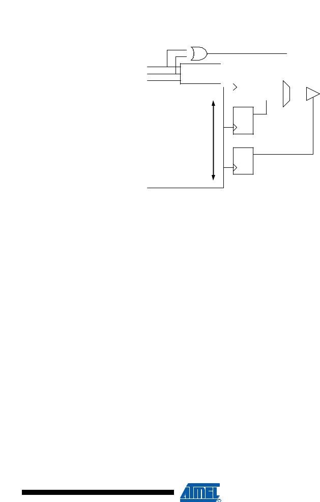
Figure 14-4. Compare Match Output Unit, Schematic
COMnx1
COMnx0 Waveform
FOCn Generator
DATA BUS
clkI/O
|
|
|
|
|
|
|
|
|
|
|
|
|
|
|
|
|
|
|
|
|
|
|
|
D Q |
|
|
|
|
|
|
|
|
|
|
|
|
|
|
|
|
|
|
|
|
|
|
|
|
|
|
|
|
|
|
|
|
|
|
|
1 |
|
|
|
|
|
|
|
|
|
|
|
|
|
|
|
OCnx |
|
|
OCnx |
|
|
0 |
|
|
|
Pin |
|
|
|
|
|
|
|
|
|
|
D Q
PORT
D Q
DDR
The general I/O port function is overridden by the Output Compare (OC0x) from the Waveform Generator if either of the COM0x1:0 bits are set. However, the OC0x pin direction (input or output) is still controlled by the Data Direction Register (DDR) for the port pin. The Data Direction Register bit for the OC0x pin (DDR_OC0x) must be set as output before the OC0x value is visible on the pin. The port override function is independent of the Waveform Generation mode.
The design of the Output Compare pin logic allows initialization of the OC0x state before the output is enabled. Note that some COM0x1:0 bit settings are reserved for certain modes of operation. See Section “14.9” on page 100.
14.6.1Compare Output Mode and Waveform Generation
The Waveform Generator uses the COM0x1:0 bits differently in Normal, CTC, and PWM modes. For all modes, setting the COM0x1:0 = 0 tells the Waveform Generator that no action on the OC0x Register is to be performed on the next compare match. For compare output actions in the non-PWM modes refer to Table 14-2 on page 100. For fast PWM mode, refer to Table 14-3 on page 100, and for phase correct PWM refer to Table 14-4 on page 101.
A change of the COM0x1:0 bits state will have effect at the first compare match after the bits are written. For non-PWM modes, the action can be forced to have immediate effect by using the FOC0x strobe bits.
14.7Modes of Operation
The mode of operation, i.e., the behavior of the Timer/Counter and the Output Compare pins, is defined by the combination of the Waveform Generation mode (WGM02:0) and Compare Output mode (COM0x1:0) bits. The Compare Output mode bits do not affect the counting sequence, while the Waveform Generation mode bits do. The COM0x1:0 bits control whether the PWM output generated should be inverted or not (inverted or non-inverted PWM). For non-PWM modes the COM0x1:0 bits control whether the output should be set, cleared, or toggled at a compare match (See Section “14.6” on page 92.).
For detailed timing information refer to ”Timer/Counter Timing Diagrams” on page 98.
93
8161B–AVR–01/09

ATmega48PA/88PA
14.7.1Normal Mode
The simplest mode of operation is the Normal mode (WGM02:0 = 0). In this mode the counting direction is always up (incrementing), and no counter clear is performed. The counter simply overruns when it passes its maximum 8-bit value (TOP = 0xFF) and then restarts from the bottom (0x00). In normal operation the Timer/Counter Overflow Flag (TOV0) will be set in the same timer clock cycle as the TCNT0 becomes zero. The TOV0 Flag in this case behaves like a ninth bit, except that it is only set, not cleared. However, combined with the timer overflow interrupt that automatically clears the TOV0 Flag, the timer resolution can be increased by software. There are no special cases to consider in the Normal mode, a new counter value can be written anytime.
The Output Compare unit can be used to generate interrupts at some given time. Using the Output Compare to generate waveforms in Normal mode is not recommended, since this will occupy too much of the CPU time.
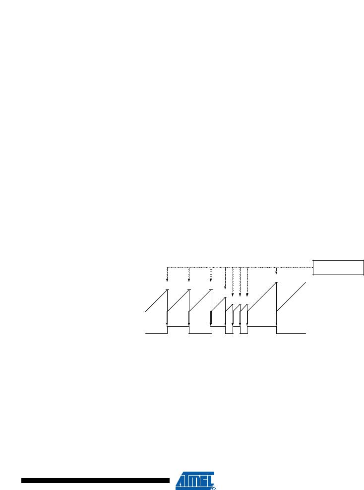
14.7.2Clear Timer on Compare Match (CTC) Mode
In Clear Timer on Compare or CTC mode (WGM02:0 = 2), the OCR0A Register is used to manipulate the counter resolution. In CTC mode the counter is cleared to zero when the counter value (TCNT0) matches the OCR0A. The OCR0A defines the top value for the counter, hence also its resolution. This mode allows greater control of the compare match output frequency. It also simplifies the operation of counting external events.
The timing diagram for the CTC mode is shown in Figure 14-5. The counter value (TCNT0) increases until a compare match occurs between TCNT0 and OCR0A, and then counter (TCNT0) is cleared.
Figure 14-5. CTC Mode, Timing Diagram
OCnx Interrupt Flag Set
TCNTn
OCn
(COMnx1:0 = 1)
(Toggle)
Period 1
2
3
4
An interrupt can be generated each time the counter value reaches the TOP value by using the OCF0A Flag. If the interrupt is enabled, the interrupt handler routine can be used for updating the TOP value. However, changing TOP to a value close to BOTTOM when the counter is running with none or a low prescaler value must be done with care since the CTC mode does not have the double buffering feature. If the new value written to OCR0A is lower than the current value of TCNT0, the counter will miss the compare match. The counter will then have to count to its maximum value (0xFF) and wrap around starting at 0x00 before the compare match can occur.
For generating a waveform output in CTC mode, the OC0A output can be set to toggle its logical level on each compare match by setting the Compare Output mode bits to toggle mode (COM0A1:0 = 1). The OC0A value will not be visible on the port pin unless the data direction for
94
8161B–AVR–01/09

ATmega48PA/88PA
the pin is set to output. The waveform generated will have a maximum frequency of fOC0 = fclk_I/O/2 when OCR0A is set to zero (0x00). The waveform frequency is defined by the following equation:
fOCnx = |
fclk_I/O |
2--------N---------(--1-----+-----OCRnx--------------------) |
The N variable represents the prescale factor (1, 8, 64, 256, or 1024).
As for the Normal mode of operation, the TOV0 Flag is set in the same timer clock cycle that the counter counts from MAX to 0x00.
14.7.3Fast PWM Mode
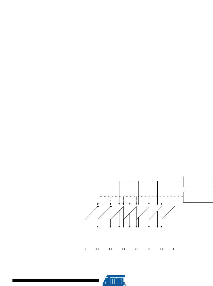
The fast Pulse Width Modulation or fast PWM mode (WGM02:0 = 3 or 7) provides a high frequency PWM waveform generation option. The fast PWM differs from the other PWM option by its single-slope operation. The counter counts from BOTTOM to TOP then restarts from BOTTOM. TOP is defined as 0xFF when WGM2:0 = 3, and OCR0A when WGM2:0 = 7. In noninverting Compare Output mode, the Output Compare (OC0x) is cleared on the compare match between TCNT0 and OCR0x, and set at BOTTOM. In inverting Compare Output mode, the output is set on compare match and cleared at BOTTOM. Due to the single-slope operation, the operating frequency of the fast PWM mode can be twice as high as the phase correct PWM mode that use dual-slope operation. This high frequency makes the fast PWM mode well suited for power regulation, rectification, and DAC applications. High frequency allows physically small sized external components (coils, capacitors), and therefore reduces total system cost.
In fast PWM mode, the counter is incremented until the counter value matches the TOP value. The counter is then cleared at the following timer clock cycle. The timing diagram for the fast PWM mode is shown in Figure 14-6. The TCNT0 value is in the timing diagram shown as a histogram for illustrating the single-slope operation. The diagram includes non-inverted and inverted PWM outputs. The small horizontal line marks on the TCNT0 slopes represent compare matches between OCR0x and TCNT0.
Figure 14-6. Fast PWM Mode, Timing Diagram
OCRnx Interrupt Flag Set
OCRnx Update and
TOVn Interrupt Flag Set
TCNTn
OCnx |
|
|
|
|
|
|
|
|
|
|
|
|
|
|
|
|
|
|
|
|
|
|
|
|
|
|
|
|
|
|
|
|
|
|
|
|
|
|
|
|
(COMnx1:0 = 2) |
|
|
|
|
|
|
|
|
|
|
|
|
|
|
|
|
|
|
|
|
|
|
|
|
|
|
|
|
|
|
|
|
|
|
|
|
|
|
|
|
|
|
|
|
OCnx |
|
|
|
|
|
|
|
|
|
|
|
|
|
|
|
|
|
|
|
|
|
|
|
|
|
|
|
|
|
|
|
|
|
|
|
|
|
|
|
|
(COMnx1:0 = 3) |
|
Period |
|
|
|
|
|
|
|
|
|
|
|
|
|
|
|
|
|
|
|
|
|
|
|
|
|
|
|
|
|
|
|
|
|
|
|
|
|
|
|
|
|
|
|
|
|
|
|
|
|
|
|
|
|
|
|
|
|
|
|
|
|
|
|
|
|
|
|
|
|
|
|
|
|
|
|
|
|
|
|
|
|
|
|
||
|
|
1 |
|
|
|
|
2 |
|
|
|
|
3 |
|
|
|
|
|
4 |
|
|
|
|
|
5 |
|
|
|
|
6 |
|
|
|
|
|
7 |
|
|
|
|
|||
|
|
|
|
|
|
|
|
|
|
|
|
|
|
|
|
|
|
|||||||||||||||||||||||||
|
|
|
|
|
|
|
|
|
|
|
|
|
|
|
|
|
|
|
|
|
|
|
|
|
|
|
|
|
|
|
|
|
|
|
|
|
|
|
|
|
|
|
The Timer/Counter Overflow Flag (TOV0) is set each time the counter reaches TOP. If the interrupt is enabled, the interrupt handler routine can be used for updating the compare value.
95
8161B–AVR–01/09

ATmega48PA/88PA
In fast PWM mode, the compare unit allows generation of PWM waveforms on the OC0x pins. Setting the COM0x1:0 bits to two will produce a non-inverted PWM and an inverted PWM output can be generated by setting the COM0x1:0 to three: Setting the COM0A1:0 bits to one allows the OC0A pin to toggle on Compare Matches if the WGM02 bit is set. This option is not available for the OC0B pin (see Table 14-6 on page 101). The actual OC0x value will only be visible on the port pin if the data direction for the port pin is set as output. The PWM waveform is generated by setting (or clearing) the OC0x Register at the compare match between OCR0x and TCNT0, and clearing (or setting) the OC0x Register at the timer clock cycle the counter is cleared (changes from TOP to BOTTOM).
The PWM frequency for the output can be calculated by the following equation:
f fclk_I/O
OCnxPWM = -----------------
N 256
The N variable represents the prescale factor (1, 8, 64, 256, or 1024).
The extreme values for the OCR0A Register represents special cases when generating a PWM waveform output in the fast PWM mode. If the OCR0A is set equal to BOTTOM, the output will be a narrow spike for each MAX+1 timer clock cycle. Setting the OCR0A equal to MAX will result in a constantly high or low output (depending on the polarity of the output set by the COM0A1:0 bits.)
A frequency (with 50% duty cycle) waveform output in fast PWM mode can be achieved by setting OC0x to toggle its logical level on each compare match (COM0x1:0 = 1). The waveform generated will have a maximum frequency of fOC0 = fclk_I/O/2 when OCR0A is set to zero. This feature is similar to the OC0A toggle in CTC mode, except the double buffer feature of the Output Compare unit is enabled in the fast PWM mode.
14.7.4Phase Correct PWM Mode
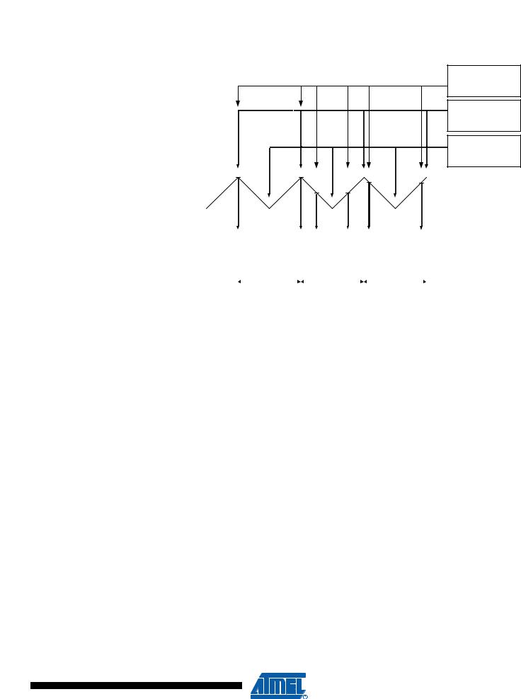
The phase correct PWM mode (WGM02:0 = 1 or 5) provides a high resolution phase correct PWM waveform generation option. The phase correct PWM mode is based on a dual-slope operation. The counter counts repeatedly from BOTTOM to TOP and then from TOP to BOTTOM. TOP is defined as 0xFF when WGM2:0 = 1, and OCR0A when WGM2:0 = 5. In noninverting Compare Output mode, the Output Compare (OC0x) is cleared on the compare match between TCNT0 and OCR0x while upcounting, and set on the compare match while downcounting. In inverting Output Compare mode, the operation is inverted. The dual-slope operation has lower maximum operation frequency than single slope operation. However, due to the symmetric feature of the dual-slope PWM modes, these modes are preferred for motor control applications.
In phase correct PWM mode the counter is incremented until the counter value matches TOP. When the counter reaches TOP, it changes the count direction. The TCNT0 value will be equal to TOP for one timer clock cycle. The timing diagram for the phase correct PWM mode is shown on Figure 14-7. The TCNT0 value is in the timing diagram shown as a histogram for illustrating the dual-slope operation. The diagram includes non-inverted and inverted PWM outputs. The small horizontal line marks on the TCNT0 slopes represent compare matches between OCR0x and TCNT0.
96
8161B–AVR–01/09

ATmega48PA/88PA
Figure 14-7. Phase Correct PWM Mode, Timing Diagram
OCnx Interrupt Flag Set
OCRnx Update
TOVn Interrupt Flag Set
TCNTn
OCnx |
|
|
|
|
|
|
|
|
|
|
|
|
|
|
|
|
|
|
|
|
(COMnx1:0 = 2) |
|
|
|
|
|
|
|
|
|
|
|
|
|
|
|
|
|
|
|
|
|
|
|
|
|
|
|
|
|
|
|
|
|
|
|
|
|
|
|
|
|
|
|
|
|
|
|
OCnx |
|
|
|
|
|
|
|
|
|
|
|
|
|
|
|
|
|
|
|
(COMnx1:0 = 3) |
||
|
|
|
|
|
|
|
|
|
|
|
|
|
|
|
|
|
|
|
||||
|
|
|
|
|
|
|
|
|
|
|
|
|
|
|
|
|
|
|
|
|
|
|
Period |
|
|
|
|
|
|
|
|
|
|
|
|
|
|
|
|
|
|
|
|
||
|
|
|
|
|
|
|
|
|
|
|
|
|
|
|
|
|
|
|
|
|||
|
|
1 |
|
|
|
|
|
2 |
|
|
|
|
|
|
3 |
|
|
|
|
|||
|
|
|
|
|
|
|
|
|
|
|
||||||||||||
|
|
|
|
|
|
|
|
|
|
|
|
|
|
|
|
|
|
|
|
|
|
|
The Timer/Counter Overflow Flag (TOV0) is set each time the counter reaches BOTTOM. The Interrupt Flag can be used to generate an interrupt each time the counter reaches the BOTTOM value.
In phase correct PWM mode, the compare unit allows generation of PWM waveforms on the OC0x pins. Setting the COM0x1:0 bits to two will produce a non-inverted PWM. An inverted PWM output can be generated by setting the COM0x1:0 to three: Setting the COM0A0 bits to one allows the OC0A pin to toggle on Compare Matches if the WGM02 bit is set. This option is not available for the OC0B pin (see Table 14-7 on page 102). The actual OC0x value will only be visible on the port pin if the data direction for the port pin is set as output. The PWM waveform is generated by clearing (or setting) the OC0x Register at the compare match between OCR0x and TCNT0 when the counter increments, and setting (or clearing) the OC0x Register at compare match between OCR0x and TCNT0 when the counter decrements. The PWM frequency for the output when using phase correct PWM can be calculated by the following equation:
f fclk_I/O
OCnxPCPWM = -----------------
N 510
The N variable represents the prescale factor (1, 8, 64, 256, or 1024).
The extreme values for the OCR0A Register represent special cases when generating a PWM waveform output in the phase correct PWM mode. If the OCR0A is set equal to BOTTOM, the output will be continuously low and if set equal to MAX the output will be continuously high for non-inverted PWM mode. For inverted PWM the output will have the opposite logic values.
At the very start of period 2 in Figure 14-7 OCnx has a transition from high to low even though there is no Compare Match. The point of this transition is to guarantee symmetry around BOTTOM. There are two cases that give a transition without Compare Match.
•OCRnx changes its value from MAX, like in Figure 14-7. When the OCR0A value is MAX the OCn pin value is the same as the result of a down-counting Compare Match. To ensure
97
8161B–AVR–01/09