

4Xilinx* 1
Table of Contents 3
Preface: About This Guide 3
About This Guide 8
Guide Contents 8
Additional Resources 9
Conventions 10
Introduction 13
Key Components and Features 13
Component Locations 19
Fast, Asynchronous SRAM 22
Address Bus Connections 24
Write Enable and Output Enable Control Signals 26
SRAM Data Signals, Chip Enables, and Byte Enables 26
Four-Digit, Seven-Segment LED Display 29
Switches and LEDs 34
Slide Switches 34
Push Button Switches 35
LEDs 36
Vga Port 36
Signal Timing for a 60Hz, 640x480 VGA Display 40
VGA Signal Timing 43
Mouse 51
Voltage Supply 53
RS-232 Port 54
Clock Sources 57
Chapter 9 58
FPGA Configuration Modes and Functions 58
FPGA Configuration Mode Settings 58
Program Push Button/DONE Indicator LED 62
Platform Flash Configuration Storage 63
Platform Flash Jumper Options (JP1) 64
“Default” Option 64
“Disable” Option 67
JTAG Programming/Debugging Ports 67
JTAG Header (J7) 68
Parallel Cable IV/MultiPro Desktop Tool JTAG Header (J5) 71
Power Distribution 72
AC Wall Adapter 72
Voltage Regulators 73
Expansion Connectors and Boards 75
Expansion Connectors 75
Expansion Boards 84
Board Schematics 85
Reference Material for Major Components 109
About This Guide
This user guide describes the components and operation of the Spartan-3 Starter Kit Board.
Guide Contents
This manual contains the following chapters:
Chapter 1, “Introduction"
Chapter 2, “Fast, Asynchronous SRAM"
Chapter 3, “ Four-Digit, Seven-Segment LED Display"
Chapter 4, “Switches and LEDs"
Chapter 5, “VGA Port"
Chapter 6, “PS/ 2 Mouse/ Keyboard Port"
Chapter 7, “RS-232 Port"
Chapter 8, “Clock Sources"
Chapter 9, “FPGA Configuration Modes and Functions"
Chapter 10, “Platform Flash Configuration Storage"
Chapter 11, “jTAG Programming/ Debugging Ports"
Chapter 12, “Power Distribution"
Appendix A, “Board Schematics"
Appendix B, “Reference Material for Major Components"
Additional Resources
For additional information, go to http:/ / support.xilinx.com. The following table lists some of the resources you can access from this website. You can also directly access these resources using the provided URLs.
Resource |
Description/URL |
Tutorials |
Tutorials covering Xilinx design flows, from design entry to verification and debugging http:/ / support.xilinx.com/ support/ techsup/tutorials/index.htm |
Answer Browser |
Database of Xilinx solution records http://support.xilinx.com/xlnx/xil ans browser.jsp |
Resource |
Description/URL |
Application Notes |
Descriptions of device-specific design techniques and approaches http:/ / support.xilinx.com/ apps/ appsweb.htm |
Data Sheets |
Device-specific information on Xilinx device characteristics, including readback, boundary scan, configuration, length count, and debugging http://support.xilinx.com/xlnx/xweb/xil publications index.jsp |
Problem Solvers |
Interactive tools that allow you to troubleshoot your design issues http:/ / support.xilinx.com/ support/ troubleshoot/psolvers.htm |
Tech Tips |
Latest news, design tips, and patch information for the Xilinx design environment http://www.support.xilinx.com/xlnx/xil tt home.jsp |
Conventions
This document uses the following conventions. An example illustrates each convention.
Typographical
The following typographical conventions are used in this document:
Convention |
Meaning or Use |
Example |
Courier font |
Messages, prompts, and program files that the system displays |
speed grade: - 100 |
Courier bold |
Literal commands that you enter in a syntactical statement |
ngdbuild design_name |
Helvetica bold |
Commands that you select from a menu |
File ^Open |
Keyboard shortcuts |
Ctrl+C |
|
Italic font |
Variables in a syntax statement for which you must supply values |
ngdbuild design_name |
References to other manuals |
See the Development System Reference Guide for more information. |
|
Emphasis in text |
If a wire is drawn so that it overlaps the pin of a symbol, the two nets are not connected. |
|
Square brackets [ ] |
An optional entry or parameter. However, in bus specifications, such as bus[7:0], they are required. |
ngdbuild [ option_name] design_name |
Convention |
Meaning or Use |
Example |
Braces { } |
A list of items from which you must choose one or more |
lowpwr ={on|off} |
Vertical bar | |
Separates items in a list of choices |
lowpwr ={on|off} |
Vertical ellipsis |
Repetitive material that has been omitted |
IOB #1: Name = QOUT' IOB #2: Name = CLKIN' |
Horizontal ellipsis . . . |
Repetitive material that has been omitted |
allow block block_name loci loc2 ... locn; |
Conventions
HXILINX
Online Document
The following conventions are used in this document:
Convention |
Meaning or Use |
Example |
Blue text |
Cross-reference link to a location in the current document |
See the section “Additional Resources” for details. Refer to “Title Formats" in Chapter 1 for details. |
Red text |
Cross-reference link to a location in another document |
See Figure 2-5 in the Virtex-II Handbook. |
Blue, underlined text |
Hyperlink to a website (URL) |
Go to http:/ /www.xilinx.com for the latest speed files. |
Chapter 1
Introduction
The Xilinx Spartan-3 Starter Kit provides a low-cost, easy-to-use development and evaluation platform for Spartan-3 FPGA designs.
Key Components and Features
Figure 1-1 shows the Spartan-3 Starter Kit board, which includes the following components and features:
200,000-gate Xilinx Spartan-3 XC3S200 FPGA in a 256-ball thin Ball Grid Array
package (XC3S200FT256) Q
4,320 logic cell equivalents
Twelve 18K-bit block RAMs (216K bits)
Twelve 18x18 hardware multipliers
Four Digital Clock Managers (DCMs)
Up to 173 user-defined I/ O signals
2Mbit Xilinx XCF02S Platform Flash, in-system programmable configuration PROM @
1Mbit non-volatile data or application code storage available after FPGA configuration
Jumper options allow FPGA application to read PROM data or FPGA configuration from other sources 0
1M-byte of Fast Asynchronous SRAM (bottom side of board, see Figure1-3) 0
Two 256Kx16 ISSI IS61LV25616AL-10T 10 ns SRAMs
Configurable memory architecture
Single 256Kx32 SRAM array, ideal for MicroBlaze code images
Two independent 256Kx16 SRAM arrays
Individual chip select per device
Individual byte enables
3-bit, 8-color VGA display port 0
9-pin RS-232 Serial Port 0
DB9 9-pin female connector (DCE connector)
Maxim MAX3232 RS-232 transceiver/translator 0
Uses straight-through serial cable to connect to computer or workstation serial port
Second RS-232 transmit and receive channel available on board test points
0
Figure 1-1: Xilinx Spartan-3 Starter Kit Board Block Diagram
PS/2-style mouse/keyboard port @
Four-character, seven-segment LED display (10)
Eight slide switches 0 Eight individual LED outputs 0 Four momentary-contact push button switches
0HXILINX
50 MHz crystal oscillator clock source (bottom side of board, see Figure 1-3) @
Socket for an auxiliary crystal oscillator clock source @
FPGA configuration mode selected via jumper settings @
Push button switch to force FPGA reconfiguration (FPGA configuration happens automatically at power-on) @
LED indicates when FPGA is successfully configured @
Three 40-pin expansion connection ports to extend and enhance the Spartan-3 Starter Kit Board @ 0 @
See www.xilinx.com/ s3board for compatible expansion cards
Compatible with Digilent, Inc. peripheral boards https:/ / digilent.us/Sales/boards.cfm#Peripheral
FPGA serial configuration interface signals available on the A2 and B1 connectors - PROG_B, DONE, INIT_B, CCLK, DONE
JTAG port 0 for low-cost download cable 0
Digilent JTAG download/debugging cable connects to PC parallel port 0
JTAG download/ debug port compatible with the Xilinx Parallel Cable IV and MultiPRO Desktop Tool 0
AC power adapter input for included international unregulated +5V power supply 0
Power-on indicator LED 0
On-board 3.3V 0, 2.5V 0 , and 1.2V 0 regulators
Component Locations
Figure1-2 and Figure1-3 indicate the component locations on the top side and bottom side of the board, respectively
.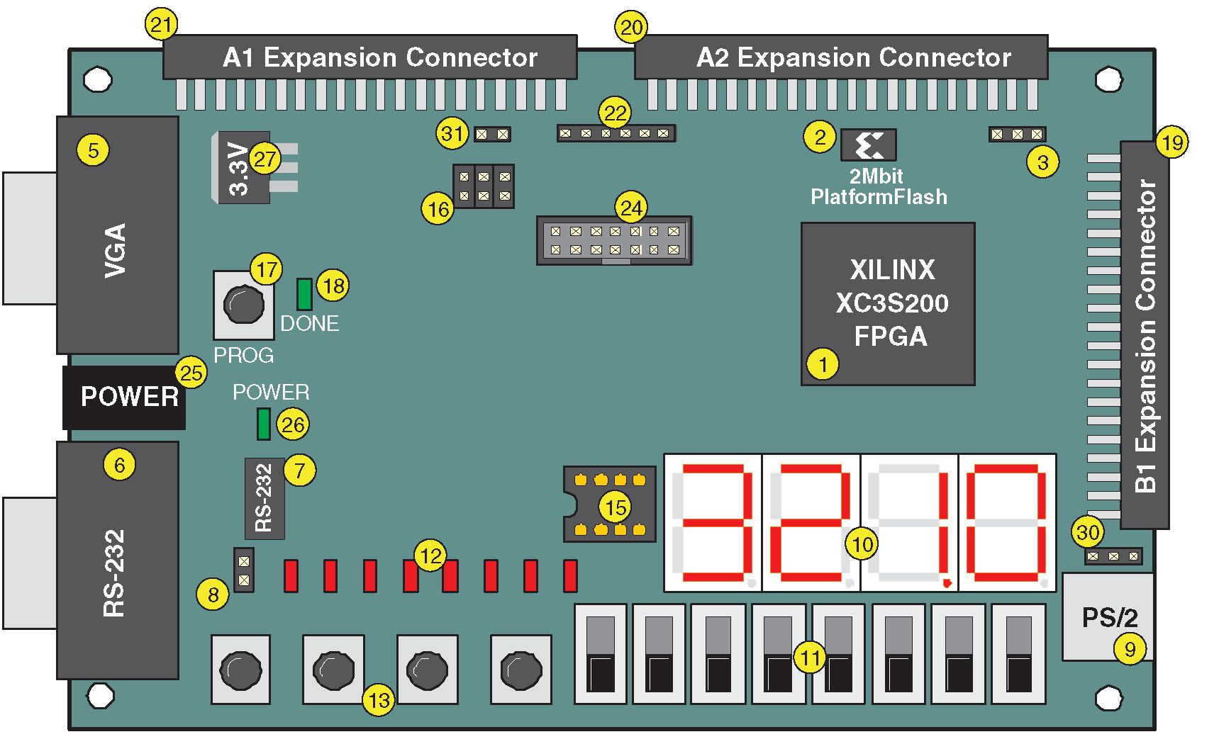
ug130_c1_02_042604
Figure 1-2: Xilinx Spartan-3 Starter Kit Board (Top Side)

ug130_c1_03_042604
Figure 1-3: Xilinx Spartan-3 Starter Kit Board (Bottom Side)
Chapter 2
Fast, Asynchronous SRAM
The Spartan-3 Starter Kit board has a megabyte of fast asynchronous SRAM, surface- mounted to the backside of the board. The memory array includes two 256Kx16 ISSI IS61LV25616AL-10T 10 ns SRAM devices, as shown in Figure 2-1. A detailed schematic appears in Figure A-8.

Figure 2-1: FPGA to SRAM Connections
UG130_c2_01_042604
The SRAM array forms either a single 256Kx32 SRAM memory or two independent 256Kx16 arrays. Both SRAM devices share common write-enable (WE#), output-enable (OE#), and address (A[17:0]) signals. However, each device has a separate chip select (CS#) control and individual byte-enable controls to select the high or low byte in the 16-bit data word, UB and LB, respectively.
The 256Kx32 configuration is ideally suited to hold MicroBlaze instructions. However, it alternately provides high-density data storage for a variety of applications, such as digital signal processing (DSP), large data FIFOs, and graphics buffers.
Address Bus Connections
Both 256Kx16 SRAMs share 18-bit address control lines, as shown in Table2-1. These address signals also connect to the A1 Expansion Connector (see “Expansion Connectors," page 51).
Table 2-1: External SRAM Address Bus Connections to Spartan-3 FPGA
Address Bit |
FPGA Pin |
A1 Expansion Connector Pin |
A17 |
L3 |
35 |
A16 |
K5 |
33 |
A15 |
K3 |
34 |
A14 |
J3 |
31 |
A13 |
J4 |
32 |
A12 |
H4 |
29 |
A11 |
H3 |
30 |
A10 |
G5 |
27 |
A9 |
E4 |
28 |
A8 |
E3 |
25 |
A7 |
F4 |
26 |
A6 |
F3 |
23 |
A5 |
G4 |
24 |
A4 |
L4 |
14 |
A3 |
M3 |
12 |
A2 |
M4 |
10 |
A1 |
N3 |
8 |
A0 |
L5 |
6 |
Write Enable and Output Enable Control Signals
HXILINX
Write Enable and Output Enable Control Signals
Both 256Kx16 SRAMs share common output enable (OE#) and write enable (WE#) control lines, as shown in Table2-2. These control signals also connect to the A1 Expansion Connector (refer to “Expansion Connectors," page 51).
Table 2-2: External SRAM Control Signal Connections to Spartan-3 FPGA
Signal |
FPGA Pin |
A1 Expansion Connector Pin |
OE# |
K4 |
16 |
WE# |
G3 |
18 |
SRAM Data Signals, Chip Enables, and Byte Enables
The data signals, chip enables, and byte enables are dedicated connections between the FPGA and SRAM. Table 2-3 shows the FPGA pin connections to the SRAM designated IC10 in FigureA-8. Table2-4 shows the FPGA pin connections to SRAM IC11.
Table 2-3: SRAM IC10 Connections
Signal |
FPGA Pin |
IO15 |
R1 |
IO14 |
P1 |
IO13 |
L2 |
IO12 |
J2 |
IO11 |
H1 |
IO10 |
F2 |
IO9 |
P8 |
IO8 |
D3 |
IO7 |
B1 |
IO6 |
C1 |
IO5 |
C2 |
IO4 |
R5 |
IO3 |
T5 |
IO2 |
R6 |
IO1 |
T8 |
IO0 |
N7 |
CE1 (chip enable IC10) |
P7 |
UB1 (upper byte enable IC10) |
T4 |
LB1 (lower byte enable IC10) |
P6 |
Table 2-4: SRAM IC11 Connections
Signal |
FPGA Pin |
IO15 |
N1 |
IO14 |
M1 |
IO13 |
K2 |
IO12 |
C3 |
IO11 |
F5 |
IO10 |
G1 |
IO9 |
E2 |
IO8 |
D2 |
IO7 |
D1 |
IO6 |
E1 |
IO5 |
G2 |
IO4 |
J1 |
IO3 |
K1 |
IO2 |
M2 |
IO1 |
N2 |
IO0 |
P2 |
CE2 (chip enable IC11) |
N5 |
UB2 (upper byte enable IC11) |
R4 |
LB2 (lower byte enable IC11) |
P5 |
To disable an SRAM, drive the associated chip enable pin High
.Chapter 3
Four-Digit, Seven-Segment LED Display
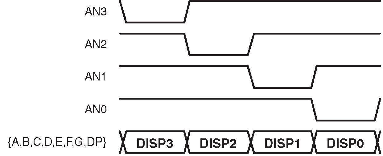
The Spartan-3 Starter Kit board has a four-character, seven segment LED display controlled by FPGA user-I/O pins, as shown in Figure 3-1. Each digit shares eight common control signals to light individual LED segments. Each individual character has a separate anode control input. A detailed schematic for the display appears in Figure A-2.
The pin number for each FPGA pin connected to the LED display appears in parentheses. To light an individual signal, drive the individual segment control signal Low along with the associated anode control signal for the individual character. In Figure 3-1, for example, the left-most character displays the value ‘2’. The digital values driving the display in this example are shown in blue. The AN3 anode control signal is Low, enabling the control inputs for the left-most character. The segment control inputs, A through G and DP, drive the individual segments that comprise the character. A Low value lights the individual segment, a High turns off the segment. A Low on the A input signal, lights segment ‘a’ of the display. The anode controls for the remaining characters, AN[2:0] are all High, and these characters ignore the values presented on A through G and DP.

UG130_c3_01_042404
Figure 3-1: Seven-Segment LED Digit Control
Table 3-1 lists the FPGA connections that drive the individual LEDs comprising a seven- segment character. Table 3-2 lists the connections to enable a specific character. Table 3-3 shows the patterns required to display hexadecimal characters
.Table 3-1: FPGA Connections to Seven-Segment Display (Active Low)
Segment |
FPGA Pin |
A |
E14 |
B |
G13 |
C |
N15 |
D |
P15 |
E |
R16 |
F |
F13 |
G |
N16 |
DP |
P16 |
Table 3-2: Digit Enable (Anode Control) Signals (Active Low)
Anode Control |
AN3 |
AN2 |
AN1 |
AN0 |
FPGA Pin |
E13 |
F14 |
G14 |
D14 |
Table 3-3: Display Characters and Resulting LED Segment Control Values
Character |
a |
b |
c |
d |
e |
f |
g |
0 |
0 |
0 |
0 |
0 |
0 |
0 |
1 |
1 |
1 |
0 |
0 |
1 |
1 |
1 |
1 |
2 |
0 |
0 |
1 |
0 |
0 |
1 |
0 |
3 |
0 |
0 |
0 |
0 |
1 |
1 |
0 |
4 |
1 |
0 |
0 |
1 |
1 |
0 |
0 |
5 |
0 |
1 |
0 |
0 |
1 |
0 |
0 |
6 |
0 |
1 |
0 |
0 |
0 |
0 |
0 |
7 |
0 |
0 |
0 |
1 |
1 |
1 |
1 |
8 |
0 |
0 |
0 |
0 |
0 |
0 |
0 |
9 |
0 |
0 |
0 |
0 |
1 |
0 |
0 |
A |
0 |
0 |
0 |
1 |
0 |
0 |
0 |
b |
1 |
1 |
0 |
0 |
0 |
0 |
0 |
C |
0 |
1 |
1 |
0 |
0 |
0 |
1 |
d |
1 |
0 |
0 |
0 |
0 |
1 |
0 |
E |
0 |
1 |
1 |
0 |
0 |
0 |
0 |
F |
0 |
1 |
1 |
1 |
0 |
0 |
0 |
HXILINX
The LED control signals are time-multiplexed to display data on all four characters, as shown in Figure 3-2. Present the value to be displayed on the segment control inputs and select the specified character by driving the associated anode control signal Low. Through persistence of vision, the human brain perceives that all four characters appear simultaneously, similar to the way the brain perceives a TV display.
UG130_c3_02_042404
Figure 3-2: Drive Anode Input Low to Light an Individual Character
This “scanning” technique reduces the number of I/ O pins required for the four characters. If an FPGA pin were dedicated for each individual segment, then 32 pins are required to drive four 7-segment LED characters. The scanning technique reduces the required I/O down to 12 pins. The drawback to this approach is that the FPGA logic must continuously scan data out to the displays—a small price to save 20 additional I/O pins
.Chapter 4
Switches and LEDs
Slide Switches
The Spartan-3 Starter Kit board has eight slide switches, indicated as 0 in Figure 1-2. The switches are located along the lower edge of the board, toward the right edge. The switches are labeled SW7 through SW0. Switch SW7 is the left-most switch, and SW0 is the rightmost switch. The switches connect to an associated FPGA pin, as shown in Table4-1. A detailed schematic appears in Figure A-2.
Table 4-1: Slider Switch Connections
Switch |
SW7 |
SW6 |
SW5 |
SW4 |
SW3 |
SW2 |
SW1 |
SW0 |
FPGA Pin |
K13 |
K14 |
J13 |
J14 |
H13 |
H14 |
G12 |
F12 |
When in the UP or ON position, a switch connects the FPGA pin to VCCO, a logic High. When DOWN or in the OFF position, the switch connects the FPGA pin to ground, a logic Low. The switches typically exhibit about 2 ms of mechanical bounce and there is no active debouncing circuitry, although such circuitry could easily be added to the FPGA design programmed on the board. A 4.7KQ series resistor provides nominal input protection.
Push Button Switches
The Spartan-3 Starter Kit board has four momentary-contact push button switches, indicated as 0 in Figure 1-2. These push buttons are located along the lower edge of the board, toward the right edge. The switches are labeled BTN3 through BTN0. Push button switch BTN3 is the left-most switch, BTN0 the right-most switch. The push button switches connect to an associated FPGA pin, as shown in Table4-2. A detailed schematic appears in Figure A-2.
Table 4-2: Push Button Switch Connections
Push Button |
BTN3 (User Reset) |
BTN2 |
BTN1 |
BTN0 |
FPGA Pin |
L14 |
L13 |
M14 |
M13 |
Pressing a push button generates a logic High on the associated FPGA pin. Again, there is no active debouncing circuitry on the push button.
The left-most button, BTN3, is also the default User Reset pin. BTN3 electrically behaves identically to the other push buttons. However, when applicable, BTN3 resets the provided reference designs.
LEDs
The Spartan-3 Starter Kit board has eight individual surface-mount LEDs located above the push button switches, indicated by 0 in Figure 1-2. The LEDs are labeled LED7 through LED0. LED7 is the left-most LED, LED0 the right-most LED. Table4-3 shows the FPGA connections to the LEDs.
Table 4-3: LED Connections to the Spartan-3 FPGA
LED |
LD7 |
LD6 |
LD5 |
LD4 |
LD3 |
LD2 |
LD1 |
LD0 |
FPGA Pin |
P11 |
P12 |
N12 |
P13 |
N14 |
L12 |
P14 |
K12 |
The cathode of each LED connects to ground via a 270Q resistor. To light an individual LED, drive the associated FPGA control signal High, which is the opposite polarity from lighting one of the 7-segment LEDs
.Chapter 5
VGA Port
Connector

Figure 5-1: VGA Connections from Spartan-3 Starter Kit Board

DB15 VGA Connector (front view)
The Spartan-3 Starter Kit board includes a VGA display port and DB15 connector, indicated as 0 in Figure 1-2. Connect this port directly to most PC monitors or flat-panel LCD displays using a standard monitor cable.
As shown in Figure 5-1, the Spartan-3 FPGA controls five VGA signals: Red (R), Green (G), Blue (B), Horizontal Sync (HS), and Vertical Sync (VS), all available on the VGA connector. The FPGA pins that drive the VGA port appear in Table5-1. A detailed schematic is in Figure A-7.
Table 5-1: VGA Port Connections to the Spartan-3 FPGA
Signal |
FPGA Pin |
Red (R) |
R12 |
Green (G) |
T12 |
Blue (B) |
R11 |
Horizontal Sync (HS) |
R9 |
Vertical Sync (VS) |
T10 |
Each color line has a series resistor to provide 3-bit color, with one bit each for Red, Green, and Blue. The series resistor uses the 75Q VGA cable termination to ensure that the color signals remain in the VGA-specified 0V to 0.7V range. The HS and VS signals are TTL level. Drive the R, G, and B signals High or Low to generate the eight possible colors shown in Table 5-2.
Table 5-2: 3-Bit Display Color Codes
Red (R) |
Green (G) |
Blue (B) |
Resulting Color |
0 |
0 |
0 |
Black |
0 |
0 |
1 |
Blue |
0 |
1 |
0 |
Green |
0 |
1 |
1 |
Cyan |
1 |
0 |
0 |
Red |
1 |
0 |
1 |
Magenta |
1 |
1 |
0 |
|
1 |
1 |
1 |
White |
VGA signal timing is specified, published, copyrighted, and sold by the Video Electronics Standards Association (VESA). The following VGA system and timing information is provided as an example of how the FPGA might drive VGA monitor in 640 by 480 mode. For more precise information or for information on higher VGA frequencies, refer to documents available on the VESA website or other electronics websites:
Video Electronics Standards Association http:/ /www.vesa.org
VGA Timing Information
http:/ /www.epanorama.net/documents/ pc/ vga timing.html
Signal Timing for a 60Hz, 640x480 VGA Display
CRT-based VGA displays use amplitude-modulated, moving electron beams (or cathode rays) to display information on a phosphor-coated screen. LCD displays use an array of switches that can impose a voltage across a small amount of liquid crystal, thereby changing light permitivity through the crystal on a pixel-by-pixel basis. Although the following description is limited to CRT displays, LCD displays have evolved to use the
Signal Timing for a 60Hz, 640x480 VGA Display
HXILINX
same signal timings as CRT displays. Consequently, the following discussion pertains to both CRTs and LCD displays.
Within a CRT display, current waveforms pass through the coils to produce magnetic fields that deflect electron beams to transverse the display surface in a “raster” pattern, horizontally from left to right and vertically from top to bottom. As shown in Figure 5-2, information is only displayed when the beam is moving in the “forward” direction—left to right and top to bottom—and not during the time the beam returns back to the left or top edge of the display. Much of the potential display time is therefore lost in “ blanking” periods when the beam is reset and stabilized to begin a new horizontal or vertical display pass.

Figure 5-2: CRT Display Timing Example
The size of the beams, the frequency at which the beam traces across the display, and the frequency at which the electron beam is modulated determine the display resolution.
Modern VGA displays support multiple display resolutions, and the VGA controller dictates the resolution by producing timing signals to control the raster patterns. The controller produces TTL-level synchronizing pulses that set the frequency at which current flows through the deflection coils, and it ensures that pixel or video data is applied to the electron guns at the correct time.
Video data typically comes from a video refresh memory with one or more bytes assigned to each pixel location. The Spartan-3 Starter Kit board uses three bits per pixel, producing one of the eight possible colors shown in Table5-2. The controller indexes into the video data buffer as the beams move across the display. The controller then retrieves and applies video data to the display at precisely the time the electron beam is moving across a given pixel.
As shown in Figure 5-2, the VGA controller generates the HS (horizontal sync) and VS (vertical sync) timings signals and coordinates the delivery of video data on each pixel clock. The pixel clock defines the time available to display one pixel of information. The VS signal defines the “refresh” frequency of the display, or the frequency at which all information on the display is redrawn. The minimum refresh frequency is a function of the display’s phosphor and electron beam intensity, with practical refresh frequencies in the 60 Hz to 120 Hz range. The number of horizontal lines displayed at a given refresh frequency defines the horizontal “retrace” frequency.