

Pattern Transfer
Once a variable height photoresist structure is created, it is subsequently used as a mask during a plasma-etching step to transfer the pattern into the underlying substrate material. For shallow structures (<10pm), reactive ion etching (RIE) can be used, while for deeper structures in silicon, deep reactive ion etching (DRIE) has become the dominant technique. The following sections will describe the basic DRIE process and how the gray-scale pattern is transferred into silicon. A detailed etch selectivity characterization for controlling the amplification of the photoresist structure into the final 3-D silicon structure will be presented.
Deep Reactive Ion Etching (drie)
Robert Bosch GmbH established the basic DRIE process in 1996 [99], where
cycles of etching and passivation are used to create deep, vertical, high aspect ratio features in silicon. Much research has been done regarding the various processes at work in the plasma, including [34, 100-107], so the basic operation is only briefly summarized below. The remaining focus will be on its application to gray-scale pattern transfer.
The starting material is typically a silicon wafer patterned with a masking material such as photoresist or silicon dioxide. A short etching step is first executed using an inductively coupled plasma (ICP) containing SF6 (and sometimes Ar or O2 gases). This etch is relatively vertical over small depths (usually <1^m), however there will be a limited amount of isotropic lateral etching of the silicon. A passivation step follows, where C4F8 gas is cycled into the chamber to create a conformal teflon-like film over the entire surface. When the etching step is repeated, the passivation layer is preferentially removed from horizontal surfaces by charged ions in the plasma, allowing vertical etching to continue. Simultaneously, this passivation layer temporarily protects the silicon sidewall from further etching by F ions and radicals. Etch and passivation steps are cycled until a desired etch depth is achieved in the silicon, resulting in a deep vertical etch with slight scalloping on the sidewalls, as shown in Figure 2.12. Etch rates of 1- 5p,m per minute are achievable.
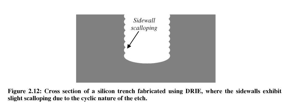
Figure 2.13 shows an example photoresist wedge on a silicon substrate. As this wedge is etched in a DRIE process, any exposed silicon will etch quickly, while the photoresist nested mask etches more slowly (the photoresist is primarily etched by ion bombardment). As the etch proceeds, the photoresist wedge will slowly recede, exposing more silicon to the high etch rate plasma. The transferred gray-scale structure will retain its original horizontal dimensions, while the vertical dimensions are amplified by the etch
selectivity. Therefore, etch selectivity control is an absolute necessity for the fabrication of precise 3D structures in silicon.