

2.3.3. Double Exposures
While the pixilated technique makes gray-scale mask design and fabrication
simple, one disadvantage is the inherent tradeoff between horizontal and vertical resolution. A small pitch will yield the best horizontal resolution, but few pixel permutations are possible, limiting vertical resolution. By choosing a large pitch, more gray-levels can be designed to fit the criteria outlined in Section 2.2.2, but the horizontal resolution in the plane of the wafer becomes poor. Even if vertical resolution is the only concern, the pitch (and therefore # of pixels) cannot be increased arbitrarily due to the finite resolution of the projection lithography system.
It is instructive to introduce typical values for each of the constraints outlined in Section 2.2.2. Using a critical pitch (Pc) of 2.5p,m and a minimum feature size (Fm) of 0.5p,m, we can calculate the minimum and maximum Tr values to be 36% and 96%, respectively. The useable range of Tr is actually even smaller in practice because pixels with Tr values above 80% are rarely realized in photoresist after development. Since the first (highest) gray level is created using Tr=36%, only approximately the bottom Уг of the photoresist thickness will have gray levels. Using a spot size (So) of 0.1p,m, only ~40 unique pixels could be designed in this range, and that requires working at the extremes of mask vendor capability, which often does not yield consistent results. And even 40 gray levels may be insufficient for MEMS structures that span 100’s of micrometers. Thus, a new method of mask design is necessary whereby high resolution in horizontal and vertical domains can be maintained, while relaxing mask fabrication tolerances.
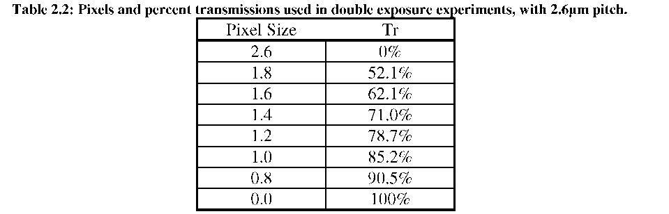
In this research, an exponential increase of photoresist gray levels has been demonstrated through the addition of a 2nd exposure step before photoresist development. By tuning the time of each of the two exposures, the entire range of photoresist can be utilized for gray-scale structure creation. A double exposure test mask was designed and fabricated to demonstrate this capability. A pitch of 2.6p,m was chosen to remain close to the diffraction limit, while Fm was increased to 0.8p,m and S0 was assumed to be 0.2p,m (both values relaxing previous mask tolerances). Only square pixels were chosen for this demonstration, yet the results can be scaled to include rectangular pixels as well. The square pixel dimensions used and their corresponding Tr values are shown in Table 2.2.
Using simply two V exposures, the number of unique exposure combinations possible with N intensity levels is N /2 (in this case, 32). Yet, by exposing with a weighted exposure technique, say 1/3 and 2/3 doses, a full complement of N intensity levels (64) can be achieved. Figure 2.11 shows measured photoresist heights for each pad in the double exposure matrix for a combination of 0.95 + 0.55 second exposures, plotted as a function of the effective total percent transmission, Treff.
![]() (18)
(18)
The large points in the figure correspond to those levels where an identical pixel was used during both partial exposures, and thus represent the gray levels possible using only a single exposure technique.
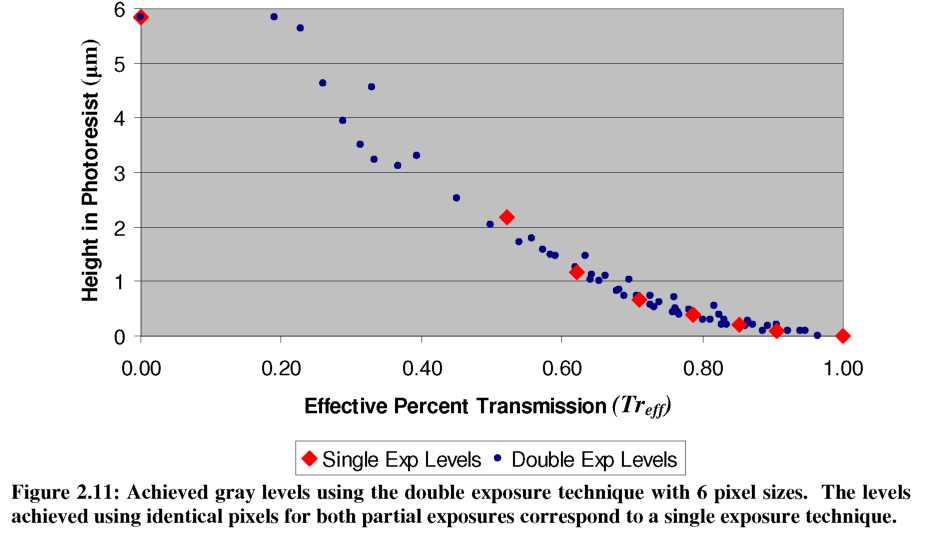
The power of this technique is easily realized when you consider that the pixel set used for this demonstration was limited to 6 square pixels with conservative spacing. Simply extending the initial pixel set to include 16 pixel permutations should result in >200 gray levels in photoresist, covering the majority of the photoresist thickness. It must also be reiterated, that these improvements can all be achieved without sacrificing any horizontal resolution.
While the design of an optical mask becomes more complicated when using the double exposure technique, empirical modeling similar to the Gaussian approximation method described in Section 2.3.1 should be possible to automate the process. Depending on the required horizontal and vertical resolution required for a particular application, the double exposure technique may or may not be necessary. However, the flexibility to create 3-D structures in this expanded design space lends further weight to the importance and significance of gray-scale technology as an enabling tool within the micro-fabrication and MEMS communities.