

Standard Lithography Process
Establishing a standard photolithography process enables the lithography processing to be considered a constant, which in turn allows all 3-D structures to be designed using only pixel selection. When developing a gray-scale lithography process, low-contrast thick photoresists are preferred to increase the range of intermediate intensities that generate different development rates, resulting in more gray levels. Clariant’s AZ9245 was chosen as the photoresist for this research because it has relatively low contrast and can be spun to a nominal thickness of >6p,m with ease. The developer solution was Clariant’s AZ400K, mixed in a concentration of 5:1, DI water to developer. This yielded development times in the 5-6 minute range, much longer than conventional development times of 1-2 minutes. Slower development steps are preferred in order to avoid over-development, which will cause a loss of lower gray levels.
Exact lithography parameters were optimized using a calibration mask [18] and the 5X projection lithography system at LPS with an observed resolution of 0.56pm, corresponding to a critical pitch of 2.8pm on the optical mask. The process details are given in Table 2.1. Note that no hard bake step is used (as suggested by the photoresist manufacturer) to avoid any photoresist re-flow during hard bake. Further details on the lithography process can be found in [14, 15, 18]. Unless otherwise noted, this gray-scale lithography process was used for processing all 3-D structures discussed in the rest of this dissertation. An example of a gray-scale photoresist wedge is shown in Figure 2.5.

Design and Lithography Advancements
The previous section established the capability to achieve multiple intermediate intensities through a pixilated gray-scale optical mask, as well as described a photoresist process to realize these intensities as differential height photoresist structures after development. To extend this work into MEMS and other applications, it was imperative that methods to control the 3-D profile’s horizontal and vertical resolution be developed, as discussed in the following sections.
Minimum Feature Limitations
The analysis and discussion provided in Section 2.2 assumes an infinitely periodic
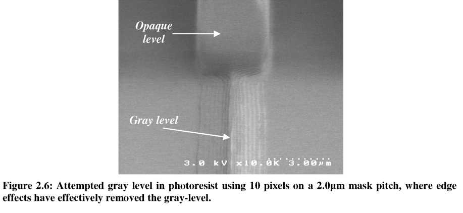
array of gray-scale pixels. However, a real MEMS structure is usually finite, leading to a definitive ‘edge’ where the pixels stop and some higher diffraction orders are collected. On large MEMS structures, this edge effect could be small compared to the overall device size, yet on smaller structures (<10p,m), the effects can be severe. Shown in Figure 2.6 is an opaque structure next to an attempted gray level, using a pitch of 2.0p,m and only 10 pixels. As evident from the SEM, the edge effects on both side of this structure effectively remove the entire intended gray level.
3-D Profile Control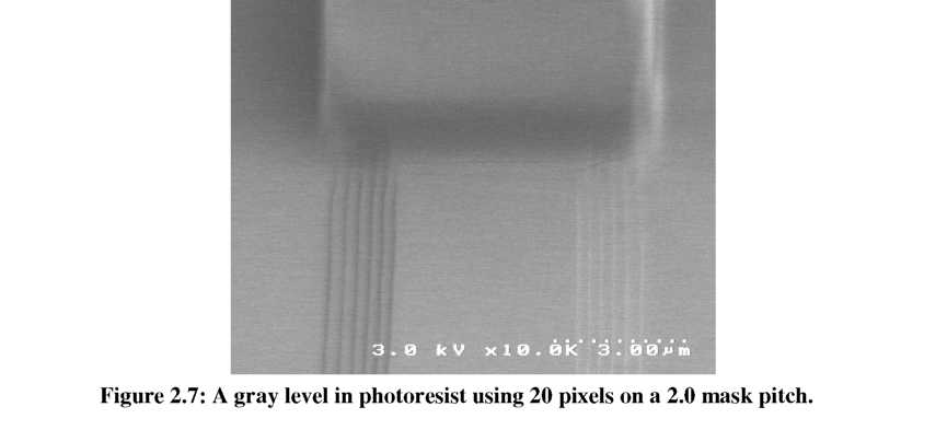
Given the small size of each pixel at the wafer level (~0.5 x 0.5pm), it is crucial
that the method developed for controlling 3-D profiles in photoresist be conducive to automation, in order to facilitate placement of the thousands of pixels required to create MEMS structures of appreciable size.
Our investigation begins with the basic law of absorption, where we know that as the incident UV light travels through the thickness of the photoresist, the intensity decreases exponentially [98]:
![]() (15)
(15)
Considering only this exponential decay of intensity through the photoresist, linear changes in transmission (i.e. I0) through an optical mask will create a logarithmic change in the exposure depth (z) at which a desired intensity is reached. Combining this logarithmic behavior with an initial uniform photoresist thickness and exposure time could determine exposure dose contours within a photoresist layer. However, there are other more factors that also influence the exact thickness of photoresist that remains after development, such as bake conditions, development rate, etc. Thus, a gray-scale profile control model must account for all these process variables.
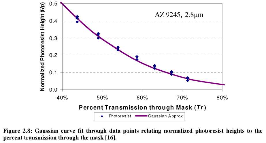
An empirical model was developed based on the use of a calibration mask and the standard optimized lithography process. The calibration mask contained long stepped structures with different constant pitch, and each contained a limited number of pixel permutations. The height of each gray level in photoresist was measured and correlated to the pixel and pitch on the optical mask that produced the particular height. Measuring multiple levels creates an empirical relation between the initial pixel size on the optical mask and the final photoresist height. Note that the exact pixel shape on the mask after fabrication is unknown, so the calculated Tr is an approximation. It is thus more important that the mask vendor be consistant than accurate because systematic errors will be accounted for in the empirical model. The normalized height in photoresist (Hp) for many pixels with the same pitch was then plotted against the corresponding Tr value, as done in Figure 2.8.
A Gaussian curve was then used to approximate the trend of these data points, creating a simple relation between any Tr and Hp [16, 18]:
![]() (16)
(16)
where A0 and у are the empirically determined fit parameters for the particular photoresist being used. Ideally, the fit parameters will be identical for different pitches, but due to approximations in Tr value and measurement uncertainty, they tend to vary slightly. A Gaussian fit to this data was chosen for two specific reasons. First, a decaying logarithm or exponential type function with intensity is expected due to the exponential decay in intensity with increasing depth. Since the intensity is proportional to тГ (Equation 10), a decaying exponential appears Gaussian when plotted against the Tr value derived from the pixel size (Equation 9). The second reason for a Gaussian curve lies in the simplicity of inverting the equation.
 (17)
(17)
When designing a specific structure, the ideal calculated Tr value is cross referenced with the available Tr values from a set of available pixels.
By using the Gaussian approximation method described above, much of the modeling behind the gray-scale lithography process may be abbreviated, and gray-scale masks may be designed to mimic any desired slope. As shown later in Section 2.5, this technique has demonstrated precise profile control over a wide range of structure sizes.