

Optical Mask Constraints
The projection lithography system used in this research was a 5 reduction stepper (CGA-Ultratech) in the clean-room facilities at the Laboratory for Physical Sciences (LPS) in College Park, MD. Since the estimated resolution of this system is between 0.5—0.6 m on the wafer, the critical pitch used on our gray-scale optical mask is on the order of 2.5—3.0 m, meaning each pixel must be even smaller. All optical masks for this research were obtained through Northrop Grumman Corp., Linthicum, MD, but the design rules discussed here can be applied to any mask vendor.
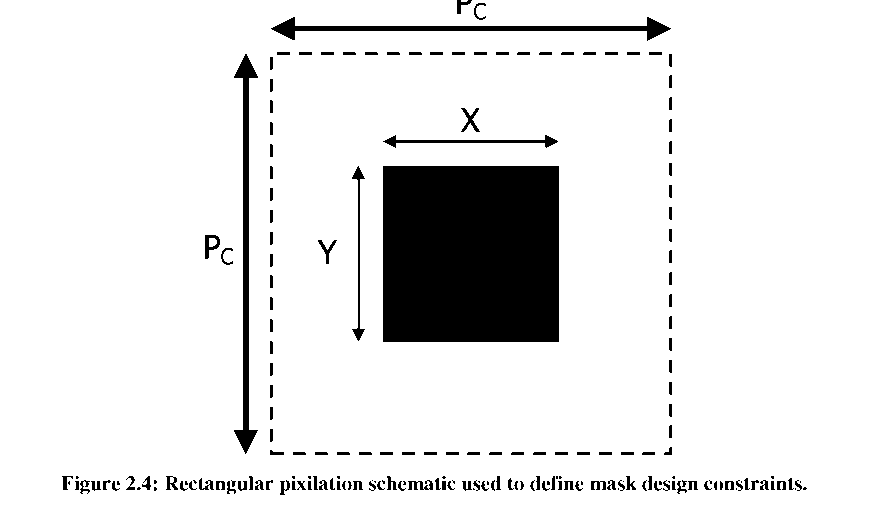
Optical masks cannot be fabricated with arbitrarily small features, so the number of different size pixels that will fit inside a particular pitch is finite. The result is a discrete set of available pixels (each with an associated transmission, Tr) that depends on the selected pitch and the mask vendor limitations. Since each pixel is sub-resolution, the actual shape of the pixel (i.e. square or circle) should not be reconstructed and therefore only the total area of the pixel should be important.
When designing a pixilated gray-scale mask, there are 2 main parameters that determine your pixel constraints: (1) minimum feature size (Fm) and (2) mask address size, usually the electron beam spot size (So). The minimum feature size is the smallest eature dimension, opaque or clear, expected to be resolved after mask fabrication (i.e. all
dimensions of an opaque box must be larger than Fm and two adjacent edges cannot be spaced closer than Fm). The spot size of the electron beam used to fabricate a mask is also important because it often defines the smallest possible increment between subsequent pixel sizes. Smaller spot sizes are advantageous because they can lead to larger pixel sets as the permutations of pixel sizes can be increased while remaining within the Fm constraints. Masks obtained from Northrop Grumman had limitations of Fm = 0.5pm and S0 = 0.1p.m.
![]() (11)
(11)
![]() (12)
(12)
![]() (13)
(13)
where PC is the critical pitch, or resolution limit, discussed earlier. The limiting case of will result in the largest transmission through the mask, while the limit of Equation 12 will define the smallest transmission through the mask. Equation 13 will determine the final number of pixels (or transmissions) available. We can now modify Equation 9 for each pixel (i) to fit the rectangular case shown in Figure 2.4:
![]() (14)
(14)
Any pixels with identical (or extremely close) Tr values may be eliminated from a pixel set since they will be redundant. One must also keep in mind that every pixel will not necessarily result in a repeatable gray level in photoresist, since the development process must be considered, which often eliminates many smaller pixels. The final pixel set will be determined through the use of a calibration mask to experimentally establish the useable range of pixels (gray levels). In some instances, a mask pitch above the critical pitch could be used for gray-scale design to increase the number of available gray-levels, but with the danger of introducing oscillations in the photoresist surface as higher diffraction orders are collected by the objective lens.