

Gray-scale Background
Before discussing advancements in gray-scale technology developed as part of this dissertation, the theoretical framework and design limitations for the chosen grayscale implementation must be discussed.
Theoretical Background
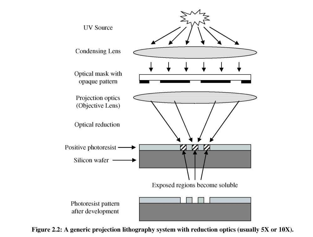
The chosen method of pixilated gray-scale lithography relies on a standard projection lithography system, a simplified schematic of which is shown in Figure 2.2. When a pixilated optical mask is placed in this system, a fraction of the incident light is blocked and transmitted light will diffract. It is this diffraction between closely spaced opaque pixels that leads to a uniform intermediate intensity at the wafer surface.
![]() (1)
(1)
and
![]() (2)
(2)
A diffraction limited optical system will cut off higher spatial frequencies in the Fourier spectrum, T’(k). Thus, the complex amplitude, A(x’), in the image plane (i.e. at the wafer surface), is given by:
![]() (3)
(3)
The parameter k refers to a lateral wave vector on the mask, whose 1st diffraction order corresponds to:
![]() (4)
(4)
where is the wavelength of illumination light used in the stepper and и is a spatial frequency of the grating lines. The numerical aperture (NA) of the system then defines the maximum angle, c, capable of passing through the system:
![]() (5)
(5)
For
normal incidence plane wave illumination, this NA
determines the critical spatial frequency, vc,
or critical pitch, pc,
necessary on the optical mask for the 1st
diffraction order to reach the critical angle, ![]() :
:
![]() (6)
(6)
For
periodic features below this critical pitch, the ±1 and higher
diffraction orders are prevented from passing through the projection
system. Since all spatial information is contained in the higher
diffraction orders, only a uniform ‘DC’ component of light (0th
diffraction order) is transmitted through the optical system, and all
spatial information regarding the shape of individual pixels is lost.
In a true lithography system, the partial coherence of the light
source,![]() ,
will also play a role in determining the critical pitch of the system
[5]:
,
will also play a role in determining the critical pitch of the system
[5]:
![]() (7)
(7)
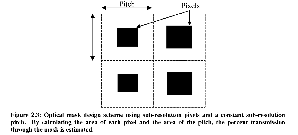
For the research performed in this dissertation, the pitch has been held constant, at or near the critical pitch in order to maintain this condition. The ‘DC’ component of the optical mask transmission was then locally modulated by varying the size of rectangular sub-resolution opaque pixels contained therein, as shown in Figure 2.3.
![]() (8)
(8)
For a pixilated approach, this integral calculates the percentage of light transmitted through the optical mask (Tr), which can be calculated using the area of each pixel (Apixel) and the area of the square pitch (Apitch):
![]() (9)
(9)
![]() (10)
(10)