

Chapter 2: gray-scale technology
This chapter will review the research performed on the core gray-scale technology process, which serves as the cornerstone of this dissertation. The developments presented here demonstrate gray-scale technology as a flexible platform for 3-D actuator development. The initial portions of this work, most notably the 3-D profile control and etch selectivity characterization, were conducted as part of my Master’s Thesis research, “Development of a Deep Silicon Phase Fresnel Lens using Gray-scale Lithography and Deep Reactive Ion Etching” [18]. For clarity, the term “gray-scale lithography’ will refer to a photolithography process using a “gray-scale optical mask,” while the term “grayscale technology” will refer to the combination of “gray-scale lithography” and a dry- anisotropic etching step used to transfer the photoresist pattern into the silicon.
Introduction
As discussed in Chapter 1, gray-scale technology is a batch fabrication technique capable of creating variable height structures in silicon using a single lithography and etching step. Gray-scale lithography was first developed for use in diffractive optics in the mid 1990’s [8, 11, 12]. One method uses commercially available high energy beam sensitive (HEBS) glass that uses the chemical reduction of silver ions in a silver-alkali-halide material to produce coloring specks of silver atoms, directly modulating the opacity of each point on a photomask [9, 10]. However, the cost of HEBS masks can be up to one order of magnitude more than standard chrome on quartz plates and there is only one known vendor, which together limit the widespread adoption of this technique. Thus, the method of gray-scale implementation chosen for this research is based on the pixilated approach described by Waits et al [14, 15], which uses many sub-resolution opaque pixels on a standard chrome optical mask in a projection lithography system.
During a UV exposure, the projection lithography system filters out all spatial diffraction orders, creating intermediate transmitted intensities proportional to the pixel size [3, 4]. Each intensity partially exposes a positive photoresist film to a certain depth. This exposure renders the top portion of the photoresist layer more soluble in a developer solution, while the bottom portion of the photoresist layer remains unchanged. Therefore, after a standard development step, an intermediate thickness of photoresist, called a ‘gray level, ’ will remain behind in areas that received a partial exposure. By locally modulating this intensity pattern with a specially designed gray-scale optical mask, many gray levels may be created at once to form a 3D structure in the photoresist, where each pixel size on the mask results in a different height gray level in photoresist.
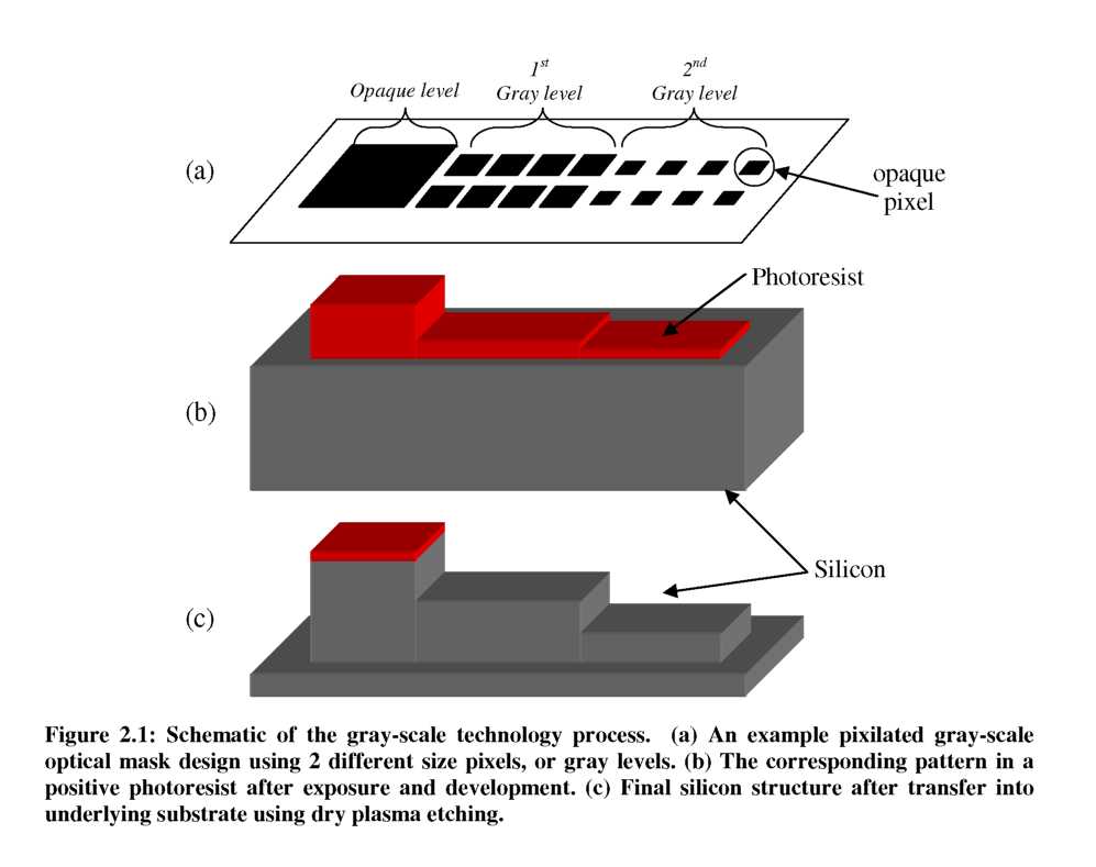
By patterning the photoresist on a silicon wafer, a dry-anisotropic etching technique, such as reactive ion etching (RIE) or deep reactive ion etching (DRIE), may be used to subsequently transfer this pattern into the silicon [2]. A schematic of this entire process is shown in Figure 2.1. By distributing many appropriately sized pixels on the optical mask, step approximations to various 3-D shapes can be replicated in the photoresist and/or underlying silicon.
The following sections will review the theoretical background of gray-scale technology, and then review developments in both lithography and etching performed during this work. Finally, three collaborations with organizations outside UMD will be presented as applications of static 3-D silicon structures fabricated using gray-scale technology.