

Future Work
The following sections will briefly comment on areas for future work based on this PhD dissertation.
Gray-scale Technology: Resolution and Uniformity
The discussion on the gray-scale technology process presented in this research
was primarily concerned with design and process control for individual devices. However, the wide acceptance of this technique will hinge upon developments in two primary areas of future work: resolution and uniformity.
As discussed briefly in Chapter 2, the horizontal resolution of gray-scale photoresist structures is limited by the pixilated technique being used during the mask design process (recall that horizontal resolution is inversely proportional to vertical resolution due to mask vendor limitations). Additionally, a finite number of pixels is required to create a distinct gray level in photoresist. The double-exposure technique introduced in Section 2.3.3 could exponentially increase the number of gray levels available without sacrificing horizontal resolution, but will require significantly more modeling and process optimization in order to reliably produce complex 3-D profiles. Another interesting possibility is to use the 2nd exposure to “sharpen” the edges of an initially defined gray-scale feature to remove edge effects from the pixilated mask design, thereby reducing the minimum gray-scale feature size.
The manufacturability of MEMS devices utilizing gray-scale technology will ultimately be limited by the uniformity and repeatability of both the lithography and etching steps. During the current research, the lithography was largely manual, allowing limited control over the uniformity. However, one area observed to have a potentially large effect on uniformity was the baking step, as soft baking photoresist on an uneven hot-plate caused dramatic differences in structure heights across the wafer. Changing to an oven soft bake could lead to more uniform photoresist solvent content and therefore developing properties, but will require significant characterization and process control. Automation of the development step should also improve wafer to wafer repeatability, although puddle techniques have been problematic due to the finite time required to cover the wafer. It is recommended that spray development techniques be investigated as an alternative.
Etching uniformity during DRIE is already a large field of interest [34, 100, 101, 105, 177-179]. In general, low silicon loading is preferred for uniformity [178] where transport is ion limited, compared to high loading that is neutral limited [100]. Groups have reported techniques for modeling uniformity effects from pattern layouts [179], or even introducing dummy structures to minimize pattern dependent processing [180]. Other research has focused on tuning the plasma for lower pressure and high coil power to improve uniformity [101]. However, each change to the layout and/or plasma process for uniformity purposes will also effect the etch selectivity of the 3-D photoresist transfer into silicon. Thus, it is suggested that a database relating etch uniformity and selectivity for high and low loading conditions be developed in order to anticipate realistic manufacturing tolerances and tuning ability when developing a device.
These interesting and exciting areas of future work on the core gray-scale technique are currently being pursued by another graduate student, Mr. Lance Mosher, as part of his Masters Thesis research (at MSAL at UMD). The author can envision developments in this fabrication technique opening up applications in micro-molding, micro-fluidics, or on-chip inductors and interconnects.
Vibrational Energy Harvesting
The voltage-tunable MEMS resonators discussed in Chapter 4 have relatively low
resonant frequencies (~2 kHz) and would likely require significant modifications for RF applications. However, the dimensions and frequencies discussed are close to those of interest in vibrational energy harvesting (100’s of Hz), an active topic of research in MEMS and distributed wireless sensor networks [141-144] .
The development and deployment of wireless sensor networks could be felt in a variety of applications, such as embedded sensors in buildings and bridges [141]. However, such systems will rely on small low power nodes that must be autonomous and maintenance free. While approaches such as micro-batteries are being investigated [181], stored power sources for applications requiring multiple years of operation are currently extremely challenging. Thus, energy scavenging approaches, such as photovoltaics and vibration harvesting, have received increasing attention. While the power available from these sources is small (typically 100’s of p,W/cm [144]), wireless RF transmitters with 10m range and <1mW power consumption have been demonstrated that rely entirely on solar and vibrationally scavenged energy [143].
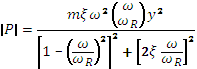
For vibrational energy harvesting, Williams and Yates [141] developed a simplified model to calculate the maximum available power (P) from a vibrational source with an angular frequency of rn (independent of power conversion technique):
 (80)
(80)
where m is the vibrating mass, Y is the amplitude of vibration, Z is a damping coefficient, and rnR is the resonant frequency of the vibrating mass.
As evident from Equation 80, the power scales with mass, so most designs seek to include the largest proof mass possible within size limitations. The power also scales with the cube of resonant frequency, and the square of amplitude, making fast high amplitude vibrations preferable for high power output (with some designs requiring stable operation for >30p,m amplitudes [141]). Near resonance, the amplitude of vibration is inversely proportional to the damping coefficient (Y ^ ), meaning low damping will lead to high power, at the expense of making the resonator more frequency selective. Other terms in Equation 80 also show that the frequency of input vibrations must match the resonant frequency of the resonator in order to maximize power. Since the frequency and acceleration of the source vibrations are inherent properties of each environment, the capability for a single node design to adapt (tune) it’s resonant frequency is quite attractive.
Looking at the vibration spectrums measured by Roundy et al [144], common ambient environments have acceleration peaks in the 100-300 Hz range. Such frequencies could be obtained using a 1000p,m silicon cube held by 3 N/m springs, giving an approximate resonant frequency of 182 Hz. In the case of large damping coefficients, this single device could cover a wide range of frequencies at the cost of dramatically reducing the power available from any particular frequency. Conversely, designs using a minimal damping coefficient could increase power dramatically, but the optimal range of frequencies for generation would be small. Thus, it would be necessary to design and fabricate many devices to be able to cover the desired range. An alternative could be to include vertically-shaped electrostatic springs to enable resonant frequency tuning (either up or down) of a single optimized design in order to maximize power output at any given frequency in the range of interest.
The paradox in such a proposal is that energy harvesting typically uses low voltages to minimize power consumption, while the electrostatic springs discussed previously in this chapter require >50V to create significant tuning. However, there are multiple potential solutions. First, reservoir capacitors could be precisely pre-charged on tuning “islands” that are isolated from the remaining system. Since the tuning mechanism is capacitive, virtually no energy should be consumed during operation and the capacitor voltage should remain stable. Note that the reservoir capacitor should be much larger than the capacitance of the comb-fingers themselves. A second option could be the inclusion of electret’s (permanent electrostatic charges), which have been shown to hold up to 100 Volts for >3 years [182]. Electrets would require corona charging as a post-processing step after resonator fabrication (possibly using shadow masks) to serve as the permanent tuning mechanism.
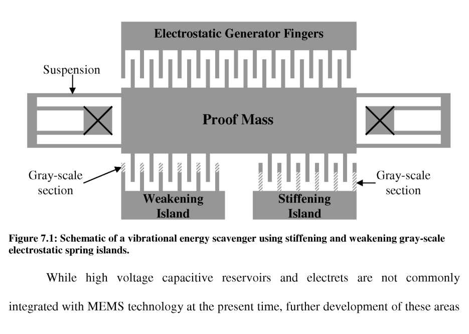
A potential tunable resonator configuration utilizing “tuning islands” and extra comb-fingers for an electrostatic generator (like the generator in [142]) is proposed in Figure 7.1. Both stiffening and weakening electrostatic fingers could be included on separate “islands” to enable tuning of the resonant frequency either up or down. This approach would enable a single optimized design to be fabricated and subsequently tuned to a final desired frequency as a post-processing step. Using the gray-scale electrostatic springs demonstrated in Chapter 4, the 182 Hz system discussed earlier could be tuned from 154 Hz (-0.85 N/m) to 227 Hz (1.66 N/m). Altering basic design parameters, such as the number of fingers and/or their spacing, could easily extend this range significantly.
Fiber Aligner Miniaturization
The device footprint of the gray-scale fiber aligner is currently large, requiring
cantilever lengths >10mm and multiple actuators measuring approximately 0.5 by 4mm. This design was initially chosen to minimize angular loss and enable the use of well understood comb-drive actuators. Yet for acceptance as a packaging technique, the layout should be more compact and compatible for array packaging. Both the fiber cantilever length and MEMS actuator size could be reduced by making some basic modifications to the design.
First, the use of a reduced cladding (RC) fiber (r=40p,m vs 62.5p,m) would have a dramatic effect on fiber spring constant because kfiber ^ radius4 (see Equation 72). Thus, an RC fiber cantilever of only 5.5mm would have the same spring constant as a 10mm cantilever of normal fiber. RC fiber is already commercially produced, often as bend- insensitive fiber (see www.StockerYale.com), making it a potentially viable solution.
A second design modification could be the migration to MEMS electrothermal actuators as the source of in-plane actuation [43-45]. Such actuators are capable of much higher forces compared to electrostatic devices, offering up to 0.67mN @ 7mA per beam
. The fabrication process for electrothermal actuators with 3-D components could be virtually identical to that used for the gray-scale electrostatic devices discussed in this research. Multiple electrothermal beam actuators could also be cascaded to increase the generated force, with the footprint still being smaller than most comb-drive designs.
Single
gray-scale fiber aligner
Figure
7.2: Schematic of compact gray-scale fiber aligner array
configuration using electrothermal v- beam actuators with attached
alignment wedges.
Methods for improving and evaluating the alignment accuracy of gray-scale fiber aligners are also of great interest, but are more related to the core gray-scale technology and equipment limitations discussed previously. This actuation mechanism could also be extended for use in other applications, such as 1 x N switches or micro-robotics.
Smaller footprints could lead towards compact fiber array packaging schemes, such as that shown schematically in Figure 7.2.
Maintaining Fiber Alignment
Once acceptable coupling has been achieved by the gray-scale fiber aligner, to
whatever tolerance is required, the device currently requires a constant application of voltage to maintain the alignment. Thus, the gray-scale fiber aligner would greatly benefit from the development of a mechanism to fix the fiber in its final position, a necessary component of any fiber packaging scheme.
There are two apparent avenues to address the fiber-fixing challenge. The first option is to immobilize the fiber via epoxy or soldering, which is typically a permanent process. Some research has been pursued to study the alignment effects on a fiber within a package caused by thermal CTE mismatch of adhesives [184] and solder ball relaxation
. Options such as laser welding could be attractive in certain cases [155], but significant research on this topic remains.
Alternatively, a mechanical locking mechanism could potentially be introduced to immobilize the silicon actuators, and therefore indirectly immobilize the fiber. MEMS bi-stable actuators [185] could be adapted to hold the comb-drive actuators, and therefore the fiber, in the final aligned positions. A schematic of such a system is shown in Figure 7.3. The primary advantage of a mechanical clamping approach is that the locking mechanism could be reversible, enabling re-positioning of the fiber if any shifts occur during or after the clamping process. However, the additional actuators would increase the size and complexity of the overall device. Significant design, simulation and testing would be required for such a mechanism, with specific focus on it’s susceptibility to shock and/or vibration.
(a) (b)
Figure
7.3: Schematic of a bi-stable clamping mechanism (a) before and (b)
after fixing a fiber actuator in an optimal position.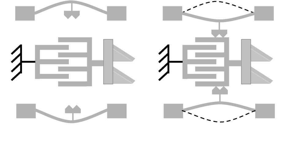
This PhD dissertation research has definitively shown that electrostatic MEMS actuators incorporating gray-scale technology have significant advantages over their planar counterparts. In demonstrating that gray-scale is a viable 3-D batch fabrication technique for developing MEMS sensors and actuators, it is my sincere hope that this technology can be leveraged by the MEMS community to develop innovative solutions to many of the technical, economic, and social challenges facing the world today.
APPENDIX A: Matlab Script for Virtual Electrostatic Spring Constants
As discussed in Section 3.3.3, the instability point of a static comb-drive actuator is defined by the perpendicular virtual electrostatic spring (ky-virtual) that is created as the voltage increases and the device deflects. To calculate this instability point, knowledge of both the actuation characteristics (V (x)) and overlap area (A(x)) as a function of displacement is required. However, for variable height profiles these relations are not simple analytical functions. Thus, a Matlab script was created to take any comb-finger height profile (h(x)) and numerically calculate ky-virtual as a function of displacement.
The script first defines all constants and assumptions about the comb actuator design (such as number of fingers and suspension spring constant). A height profile is then input from a text file, where it is assumed that the height profile accounts for fringing fields by scaling the physical height into an “effective” height representing dC/dx. Equation 43 is then evaluated numerically to obtain A(x), while V (x) is calculated numerically using the piecewise constant technique of Equations 36 and 37. Finally, the virtual spring constant ky-virtual(x) as a function of displacement is calculated using Equation 46. The code is shown below with comments in green font.
% Matlab code for calculating the perpendicular virtual electrostatic spring constant as a % function of displacement for arbitrary comb-finger profiles
% Define constants and design assumptions in SI units
step = 1;
stepx = 1e-7;
epsilon = 8.85e-12;
gap = 10e-6;
num_fingers = 200;
k = 5;
max_finger_height = 100e-6;
% Input “effective” height profile from text file - can account for fringing fields
string_input = 'height_profile.txt';
fid = fopen(string_input);
height = fscanf(fid, '%f,[1 inf]);
height = height';
fclose(fid);
% Calculate overlapping area as a function of (x) by integrating over the height profile % Corresponds to A(x) in Equation 43 area(1) = max_finger_height * stepx; for(ii=2:length(x))
increment = x(ii) - x(ii-1); area(ii) = area(ii-1) + height(ii) * increment; end
2 2 % Calculate voltage vs. displacement characteristics for V (x) in Equation 45
% Assumes force is proportional to the given “effective” height profile
Vtemp2 = zeros(length(x),1);
= zeros(length(x),1);
V2 = zeros(length(x),1);
for(n = 2:length(x));
increment = x(n) - x(n-1);
Vtemp2(n) = increment * gap * K / (epsilon * height(n)) / num_fingers;
V(n) = sqrt(V(n-1)A2 + Vtemp2(n));
V2(n) = V(n) * V(n); end
% Use A(x) and V (x) in Equation 46 to calculate the virtual electrostatic spring as a
% function of displacement, ky(x)
for(i=1:length(area))
ky(i) = num_fingers * epsilon * area(i) * V2(i) * 2 / gapA3; end
plot(x,ky)
APPENDIX B: Process Flow for Gray-scale SOI process
The process flow for integrating gray-scale technology within an SOI actuator required significant development. The final process was described qualitatively in Section 3.5 and the details are shown in Table B.1. The gray-scale lithography and DRIE steps were described in more detail elsewhere in this dissertation (see Chapter 2). Slight modifications would be required to adapt this process to devices having different layouts or requiring different etch selectivity.
The wafer saw step is intentionally performed before the wet oxide etch release step to maintain structural integrity during the relatively harsh sawing process. The oxide etch release required significant development as the sequence of etching in buffered oxide etch (BOE) and rinsing in DI water often effected the complete etching between high aspect ratio features. In general, 1-2 rinse steps in DI water (5 min each) helped to ensure complete undercutting of desired structures. The final die rinse process was a combination of multiple soaks in DI, followed by soaks in IPA to avoid stiction problems (due to its low surface tension).
1 As of 1/14/06 (http://www.analog.com/en/cat/0,2878,764,00.html)