

Fabrication
Figure
5.13: (a) Optical and (b) close-up SEM micrographs of photoresist
gray-scale alignment wedges using а
3.2цт
pitch.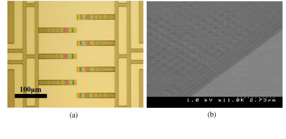
The fabrication of the gray-scale fiber aligner follows the same gray-scale SOI comb-drive process flow presented previously in Chapter 3 (hence both fiber aligners and comb-drives can be fabricated simultaneously). Figure 5.13 shows optical and SEM micrographs of fabricated gray-scale alignment wedges in photoresist. In Figure 5.13(a), the opposing wedges appear with rainbow colors that are indicative of the changing photoresist thickness. The small holes evident in the wedge in Figure 5.13(b) are caused by partial re-construction of the pixels on the optical mask since the chosen pitch (3.2pm) is slightly above the projection lithography system resolution (a tolerable effect in our current application).
slope, as expected from Figure 5.12(b), where micron-level roughness has been achieved over the majority of the slope. Note that the holes in photoresist shown previously in Figure 5.13(b) are not evident in the silicon after DRIE pattern transfer. Due to the size and location of the wedges, profilometer tips could not reliably trace the alignment finger profiles, and white light interferometry did not capture sufficient reflected light from the angled surface. Thus, quantitative roughness measurements were impractical without destructive testing that makes it impossible to relate roughness to device performance.
Assembly
To prepare the sample for testing, a length of single mode optical fiber (Corning SMF-28e) was manually stripped and cleaved. The cleaved free end of the fiber is placed between the alignment wedges (attached to the comb-drives), while the bulk of the fiber passes through the static trench. In order to enable coupling to other devices (either optical fibers or indium-phosphide (InP) waveguides), the cleaved facet of the fiber cantilever hangs slightly off the edge of the SOI chip (<1mm).
The bulk fiber is secured in the static trench with UV-curing epoxy (Norland Products, Inc.) to create a flexible cantilever. Small drops of epoxy are applied using a piece of optical fiber dipped in un-cured epoxy. Due to the lack of control over drop volume, the UV lamp must shine on the sample immediately after the drop is applied to avoid excessive spreading of the epoxy. The effect of spreading epoxy is most noticeable when it wicks along the bottom of the fiber beyond the static trench, effectively shortening the fiber cantilever length. Since the extents of epoxy flow are easily viewed under a microscope, an adjusted fiber cantilever length can be estimated to account for this effect. A device after fiber attachment is shown in Figure 5.16.
Since the fiber attachment process is entirely manual, it is difficult to ensure that the fiber touches both wedges in its rest state. Reliable operation can be achieved with small gaps between the wedge and fiber, but requires a voltage offset to move both sets of wedges into contact before the fiber begins to move. The inconsistencies with manual fiber attachment and epoxy dispensing should be remedied by moving towards automated pick and place machines with controlled liquid dispensing capabilities [164]. Alternative methods for fiber attachment, such as laser spot welding could also be investigated [165].
(b)
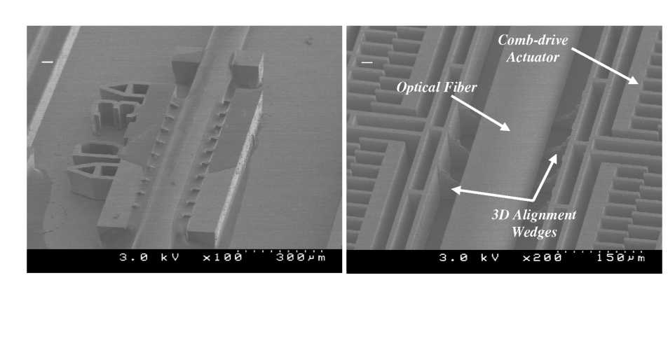 Figure
5.16: SEM’s of (a) fiber secured in the static trench with
UV-curing epoxy and (b) the free end resting between the 3-D
alignment wedges.
Figure
5.16: SEM’s of (a) fiber secured in the static trench with
UV-curing epoxy and (b) the free end resting between the 3-D
alignment wedges.