

Passive Techniques
For the purposes of this research, ‘passive’ alignment techniques will refer to methods where the final alignment and assembly is performed without any light propagating in the optical path. Essentially, the goal is to fabricate and assemble all components extremely accurately and hope that the result is acceptable when the light is turned ‘on.’ Since the 1970’s, anisotropically etched v-grooves in silicon have been used to create precise optoelectronic packaging platforms for passive alignment of an optical fiber to optoelectronic components [78—83]. The boundaries of the v-groove are defined during the lithographic process to be precisely aligned with other features on the wafer, forming what is commonly called a “silicon waferboard,” as shown in Fig. 1.4 [81]. The optical fiber is secured in the v-groove, while optoelectronic chips are flip-chip bonded to pre-fabricated solder pads, often using surface tension for self-alignment of the chip and substrate, see Fig. 1.5 [84].
By maintaining strict fabrication and assembly tolerances, such approaches report alignment in the range of 1—2 m [81, 82], which will not meet the needs for future devices that will require sub-micron tolerances [85]. Limiting factors often include the tolerance of fiber diameter, core/cladding concentricity, and imperfect mounting in the V- groove [83]. An additional challenge to such v-groove/flip-chip approaches is to control the vertical alignment of each component, as vertical shifts due to changes in solder ball/paste volume are common.
Even if these challenges can be overcome, such passive alignment schemes rely on extremely precise fabrication tolerances to cumulatively guarantee alignment, which can significantly increase processing costs. Therefore, an attractive alternative approach is to relax fabrication and assembly tolerances and instead use on-chip actuation to optimally position each fiber for maximum coupling - essentially performing the role of the expensive macro-aligner at the micro-scale.
Active Techniques
Active fiber alignment involves monitoring the amount of coupled power through
t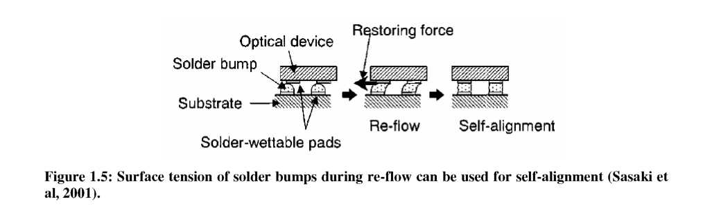 he
system while changing the location of the optical fiber. The fiber is
then fixed at the location where maximum coupling is measured. The
primary benefits of on-chip active alignment systems using MEMS are:
he
system while changing the location of the optical fiber. The fiber is
then fixed at the location where maximum coupling is measured. The
primary benefits of on-chip active alignment systems using MEMS are:
Relaxed fabrication and assembly tolerances: Final alignment is no longer solely dependent on cumulative fabrication tolerances of multiple components, reducing the required accuracy of individual components
Potentially high-volume and high throughput: actuation mechanisms are batch fabricated and contained inside each optoelectronic module, enabling individually optimized alignment
Sub-micron actuation capability: MEMS actuators with sub-micron displacement resolution are common.
Multiple on-chip active fiber alignment systems using MEMS approaches have been proposed and demonstrated, using a variety of actuation schemes. Alignment in the plane of the wafer (1-D) has been achieved using electrothermal actuators [86, 87] or asymmetric laser trimming of films with residual stress [88]. However, as with the passive alignment techniques, the lack of vertical actuation capability is extremely limiting. Kaneko et al provided a small amount of vertical shift by using a partially metal coated fiber in a V-groove, yet the rotation of the fiber was done externally and the motion was discrete (only 4 separate points could be reached) [89].
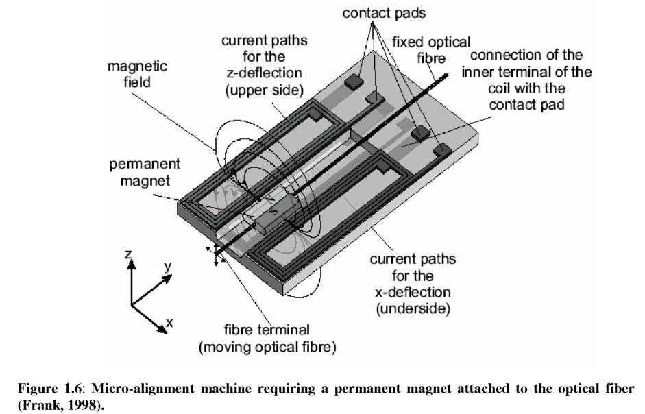
When it comes to MEMS devices providing multi-axis alignment, there have been three primary devices developed. An electromagnetic-based actuator was developed by T. Frank, shown in Figure 1.6, that was capable of deflecting an optical fiber cantilever over 100^m [90, 91]. The actuator used large coils in a multiple wafer stack to actuate a permanent magnet attached to the end of the fiber. However, this technique requires the attachment of a permanent magnet to the fiber, making this technique impractical as a high volume, high-throughput packaging option.
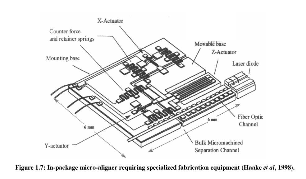
In contrast, electrostatic comb-drive actuators with 3-D shaped components could provide an on-chip actuation packaging platform capable of high-resolution active optical fiber alignment within an optoelectronic module in both the in-plane and out-of-plane directions. Such a system could be batch fabricated in potentially dense configurations, would require no previous fiber preparation, and could be integrated with 3-D gray-scale actuators for tailoring displacement/alignment resolution. The principles, design, fabrication and testing of the on-chip 2-axis MEMS fiber alignment system developed in this work are discussed in Chapters 5 and 6 of this thesis.