Tailored Comb-finger Design and Simulation
To meet a specific resolution, we see that the actuator design can be adjusted through many parameters (suspension, gap, etc). However, in order to meet a required resolution at large displacement, we see that the resolution at small displacements will far exceed that which is necessary. This means we are essentially “wasting” voltage during small displacements of the device since we unnecessarily created extremely high resolution at those points. Ideally, a constant resolution over the entire range would be the most effective use of applied voltage. Thus, the resolution at large displacements should be improved while keeping the resolution at small displacements unchanged.
Since traditional planar comb-drives use a constant gap between the moving and stationary fingers, they have a constant change in capacitance per unit length and generate a force that is independent of the relative finger position. However, by locally modifying the capacitance profile, the force-engagement profile can be changed, enabling the resolution to be tailored as the displacement changes. For example, as the voltage is increased, the generated force scales as V. If the change in capacitance (i.e. force) decreased as the actuator is displaced, the effect of squaring the voltage (V ) would be offset. The net effect would be the improved resolution at large deflections without overengineering small displacements.
As mentioned in Chapter 1, previous approaches for tailoring the capacitance (and force) characteristics have varied the gap, d^d(x), between the moving and fixed comb- fingers. However, such variable-gap approaches cause large increases in the wafer real- estate required for each comb-pair (frequently >50%), resulting in a much larger device footprint [60, 61]. One group realized that with a variable height profile, h^h(x), the generated electrostatic force can also be made position dependent without increasing
device footprint. They expanded their simulated designs to include shaping in the vertical dimension, yet eventually conceded that their designs could not be fabricated due to manufacturing limitations [62].
The following sub-sections describe new 3-D comb-finger designs that use grayscale technology to locally reduce the height of comb-fingers to alter the capacitance profile, as shown in Figure 3.4. Such an approach does not increase the area occupied by each comb-pair, while enabling similar tuning of displacement-voltage profiles. Both analytical and finite element analysis will be used to investigate the effects of shaping comb-drive components within the constraints of gray-scale technology. To enable the extension of these actuators to the optical fiber alignment systems developed in Chapters 5 and 6, 100p,m silicon-on-insulator (SOI) wafers will be considered.
Analytical Displacement Simulations (2-d)
To further establish the intuition for tailoring comb-fingers, analytical simulations using 2-D parallel plate approximations for the capacitance were used. This method was then extended to simulate the displacement-voltage behavior of a profile given a position dependent capacitance change (dC/dx) [134]. Much of the analysis and designs will use 10:1 aspect ratios, which are readily achievable in DRIE, making the initial gap=10p.m for 100p,m SOI wafers. Determining the displacement-voltage characteristics of a comb- drive design starts by estimating the capacitance at each position of an individual comb- pair. The device behavior is then calculated by using an incremental method to determine the voltages required to create small displacements.
Let us consider our proposed design which locally varies the height of each comb- finger using gray-scale technology, h^h(x). The static displacement, Ax(V), of this comb-drive is the point at which the generated comb-drive force and the restoring spring force are equal in magnitude. Assuming a linear spring constant, k, the displacement of a planar comb-drive was easily described as a quadratic function of applied voltage and linearly proportional to the other design parameters in Equation 30, and is repeated here using a height that changes with position, h(x):
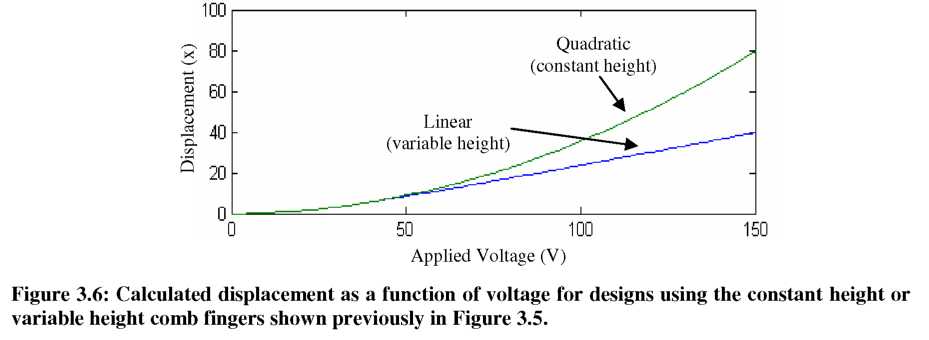
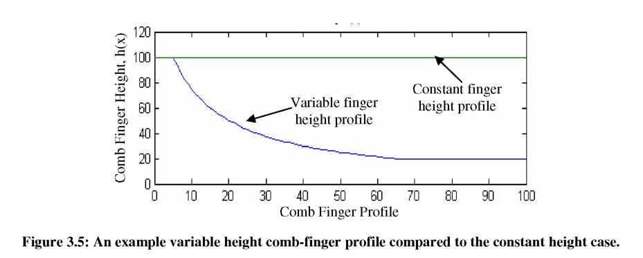
Looking at Equation 34, we see that by changing the height profile of the comb-finger to scale as the inverse of displacement (h(x) ^ 1/Ax) will create a relationship where both displacement and voltage scale together quadratically:
![]() (35)
(35)
An example of a (1/Ax) profile is shown in Figure 3.5. Essentially, as the displacement (Ax) increases with voltage, the height (h) decreases to offset the squaring of the applied voltage. This decrease in height is analogous to the gradual increase in gap between comb-fingers investigated by other groups [60, 61], but in our case the overall device footprint remains unchanged. Similarly, the opposite effect can be produced by creating comb-fingers that gradually increase in height to give cubic or other force/displacement profiles (analogous to decreasing the gap).
![]() (36)
(36)
A running calculation of voltages is then used to assemble the voltage as a function of displacement, where AVi is typically 0.1V:
![]() (37)
(37)
Using a parallel plate approximation, we initially assume the change in capacitance with position (dC/dx) to simply be proportional to the local height of the moving comb-finger, h(xi). Figure 3.6 shows simulated displacement characteristics for