

2.5.2.1. Compensated Aspect Ratio Dependent Etching (carde)
My research on silicon PFLs with decreasing ridge width and focal length
revealed that aspect ratio dependent etching (ARDE) [34, 102, 106] caused significant changes in overall profile accuracy, as small ridges at large radii did not etch as deeply as larger ridges towards the center [16]. This problem is expected to limit future PFL efficiency because the annular ring created by each ridge has an identical collection area, so the accuracy of small outer ridges dominates PFL performance. Since gray-scale technology is already being employed to define the vertical dimensions of the PFL features, a photoresist biasing technique using gray-scale lithography was created to counteract the subsequent ARDE. Specifically, a vertical bias was introduced to the design of variable-height photoresist nested masks to locally modulate etching time according to feature size and pattern density, creating a compensated aspect ratio dependent etching (CARDE) process [36, 125].
The conventional, or uncompensated, PFL profile thickness profile, t(r), given a desired focal length of 17.1m and 6.4 keV photons, can be defined as [36]:
![]() (22)
(22)
which normalizes the periodic modulo function to the maximum photoresist height (PRmax) available in the design. An investigation of Equation 22 reveals that as the radius increases, each ridge becomes thinner and thus has a higher aspect ratio.
For the CARDE PFL, a compensating function (S(r)) was introduced to the above design. Since the widths of the PFL ridges steadily decrease as the radius increases, a linearly decreasing compensation function was used for simplicity:
![]() (23)
(23)
where Rmax is the radius at which no compensation will be used and S0 is the maximum normalized offset in the center (r=0) of the PFL. The compensation function is then incorporated into the thickness profile of Equation 22:
![]() (24)
(24)
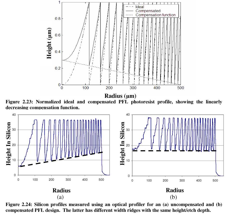
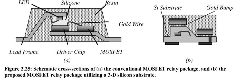
An example of the normalized compensated and uncompensated PFL profiles is shown in Figure 2.23. The large, fast-etching ridges at the center of the lens are now defined using higher gray levels (i.e. thicker photoresist). These large central ridges will begin etching after a delay, while the thin outer ridges will begin transferring into the silicon immediately, effectively getting a head start. At a certain point later during the etch, the large central ridges will catch up to the thin outer ridges and a consistent etch depth/ridge height will be achieved. This behavior is confirmed in the two silicon PFL profiles shown in Figure 2.24. For the uncompensated case, the ridge height/depth decreases at large radii as the aspect ratio increases. However, for the CARDE case, a consistent ridge height/depth is achieved.
This photoresist biasing technique clearly offers the ability to control the vertical dimensions of a 3D silicon profile despite changes in feature size that causes different etch rates across the pattern. Such a technique could be utilized for the integration of gray-scale structures with silicon-on-insulator (SOI) actuators, since electrostatic MEMS actuators often incorporate a wide range of feature sizes and over-etching of large features, gray-scale or otherwise, may be undesirable.
3-D Substrates for Packaging (Toshiba)
Researchers at the Toshiba Corporation (Corporate Manufacturing Engineering
Center, Yokohama, Japan) desired to reduce the size of their metal-oxide-semiconductor field effect transistor (MOSFET) relay - a switching device for small electrical signals
commonly used in measurement equipment. Therefore, a new, smaller MOSFET relay package configuration based on a 3-D silicon substrate was proposed and demonstrated using gray-scale technology at UMD [126, 127].
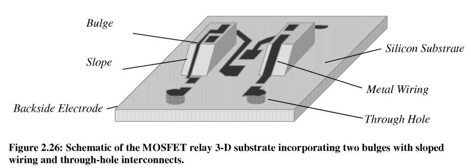
The outline of a conventional MOSFET relay package, shown in Figure 2.25(a), contains three separate devices: a light emitting diode (LED), the MOSFET, and the Driver chip. Traditionally, the chips are connected by wire bonding and the package is shielded by plastic molding. The proposed relay package, at approximately one-half the size of the conventional package is shown in Figure 2.25(b). The combination of a 3-D silicon substrate (in place of the lead-frame) and flip-chip bonding to connect the MOSFET and Driver chips enables more dense packing of the components to reduce overall package size by 50%.
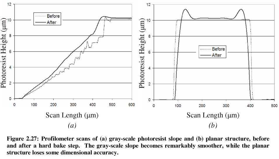
The basic design of the 3-D substrate is shown in Figure 2.26. The substrate has three primary features. First, backside electrodes are connected to the substrate surface using large through-hole interconnects. Second, two large bulges are used to provide a vertical platform for attaching the Driver chip above the LED. And third, electrical connection between the top and bottom of the bulges is accomplished by patterning wires on a large, sloped surface on the side of the bulges.
The major fabrication challenge is to optimize the gray-scale technology process to achieve sloped wiring connections between multiple levels vertically separated by >100p,m. The primary concern for developing sloped interconnects is the surface morphology of the slope, since a single large step could prevent electrical continuity.
Using a minimum spot size of S0=100nm as the increment in pixel width or length, a set of >50 pixels was created for a pitch of 3.0p,m on the mask. Using a fixed increment in pixel width creates a change in pixel area proportional to its length (AArea = Increment x Length), and vice versa. Thus, there will be a large increment in pixel area between two large pixels, creating larger gray level steps at the top of photoresist structures (this was also apparent previously in Figure 2.11). Since a single gray level step of only a few micrometers could prevent electrical connection down the tall
(>100pm) gray-scale slope, post-processing of the photoresist and silicon slopes was investigated.
A hard-bake step was added to a 10pm version of the gray-scale lithography process (following the development step) in an attempt to cause limited photoresist reflow and improve the smoothness of the slope. Figure 2.27 shows profilometer scans of two photoresist structures before and after the hard bake step.
These photoresist profiles were subsequently transferred into silicon, where the average roughness on the gray-scale slopes immediately after DRIE was measured to be less than 50nm. Simple post-processing steps, such as isotropic plasma etching and thermal oxidation, have been used to further improve the sloped surface morphology. Alternative methods, such as hydrogen annealing [129], could be used for dramatic smoothing of the silicon profile if desired.
The final step in developing 3D sloped interconnects was to define metal traces on the slope and verify electrical continuity. A Ti/Au (60nm/300nm) layer was evaporated over the entire substrate. Since the substrate has already undergone DRIE, photoresist spray coating was performed at the Toshiba Corporate Manufacturing Engineering Center in Yokohama, Japan to coat the complex topography. Contact lithography was used to pattern this photoresist layer and wet etching removed the excess metal, leaving various metal traces on the 3-D substrate, as shown in Figure 2.28(a).
Electrical continuity was verified between the top of this 170pm tall bulge and the bottom of the etched open area, using standard wafer probes. These results confirm that the final gray-scale silicon slope was sufficiently smooth for even a thin (360nm) metal layer. Figure 2.28(b) shows example IC’s after flip-chip bonding, demonstrating the ability to interconnect multiple IC’s at different elevations on the same substrate.