Phase Fresnel Lens (nasa)
A phase Fresnel lens (PFL) is essentially a small grating that will diffract incident radiation towards its focus, while ideally producing a phase change within each grating zone to concentrate all incident power into the primary focus. Recently, G. Skinner proposed a Fresnel lens-based system for astronomical observations at hard X-ray and gamma-ray energies [115-117]. This system would have the highest diffraction-limited angular resolution of any wavelength band, resulting in a greater than 10 improvement over current gamma-ray imaging systems. The sensitivity of the proposed system would also be tremendous compared to typical background-limited gamma-ray instruments, 3 resulting in a 10 improvement. (Improvements based upon comparison of a 5m Fresnel lens-based system to that of INTEGRAL [117].) The main drawback is the inherently long focal length, on the order of 106 km, requiring that the lens and detector be located on separate spacecraft and aligned appropriately. (A detailed mission study indicated that given current propulsion technology, a large focal length is not prohibitive [118]).
To demonstrate the superior imaging properties of a PFL, scaled down lenses were developed for ground testing at lower X-ray energies as part of my masters thesis work [16, 18]. The thickness (t) of a PFL, as a function of radius (r), is defined as [119]:
![]() (19)
(19)
where 12n is the thickness of material required to produce a phase shift of 2n, and A is a function of focal length f) and target photon energy (E), given by:
![]() (20)
(20)
Neglecting absorption effects, the lens profile can also be extended to higher phase depths, such as 4n, 6n, etc [120]. Making a step approximation to the ideal profile leads to an expression for the efficiency (nLens) of a multi-level diffractive lens, given the number (N) of steps used to approximate the profile [121-123]:
![]() (21)
(21)
Therefore, a traditional binary lens (2 steps) has a maximum theoretical efficiency of 40.4%. For example, By increasing the number of steps using gray-scale technology to 8, the maximum theoretical efficiency reaches 95.0%.
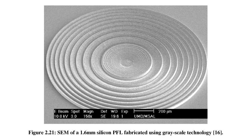
Using the photoresist profile and etch selectivity control methods described earlier, silicon PFL’s with diameters as large as 4.7mm were designed and fabricated. Figure 2.20 shows an optical profiler scan of a fabricated silicon PFL profile (red) along with the designed profile (blue). The close agreement over the measured profile, demonstrates the precise profile control possible using the gray-scale techniques developed in this research. A phasor-based profile evaluation method was developed in combination with optical profiler scans of silicon PFL profiles to estimate the efficiency of the fabricated structures [18, 36]. Efficiencies of >87% were obtained for 1.2mm diameter PFL’s assuming 8.4keV photons and f=118m [18]. An SEM of a 1.6mm diameter silicon PFL is shown in Figure 2.21 [16].