

Selectivity Characterizations
Precisely controlling the vertical scaling of the photoresist into the final silicon structure (i.e. etch selectivity) during DRIE is one of the major challenges in the grayscale technology process. Many factors contribute to the etch rate of both the silicon and photoresist, and often the effects are difficult to de-couple entirely. During each etch cycle of DRIE, the silicon is etched by a combination of chemical reactions and ion- assisted etching, while the photoresist is etched by sputtering via ion bombardment.
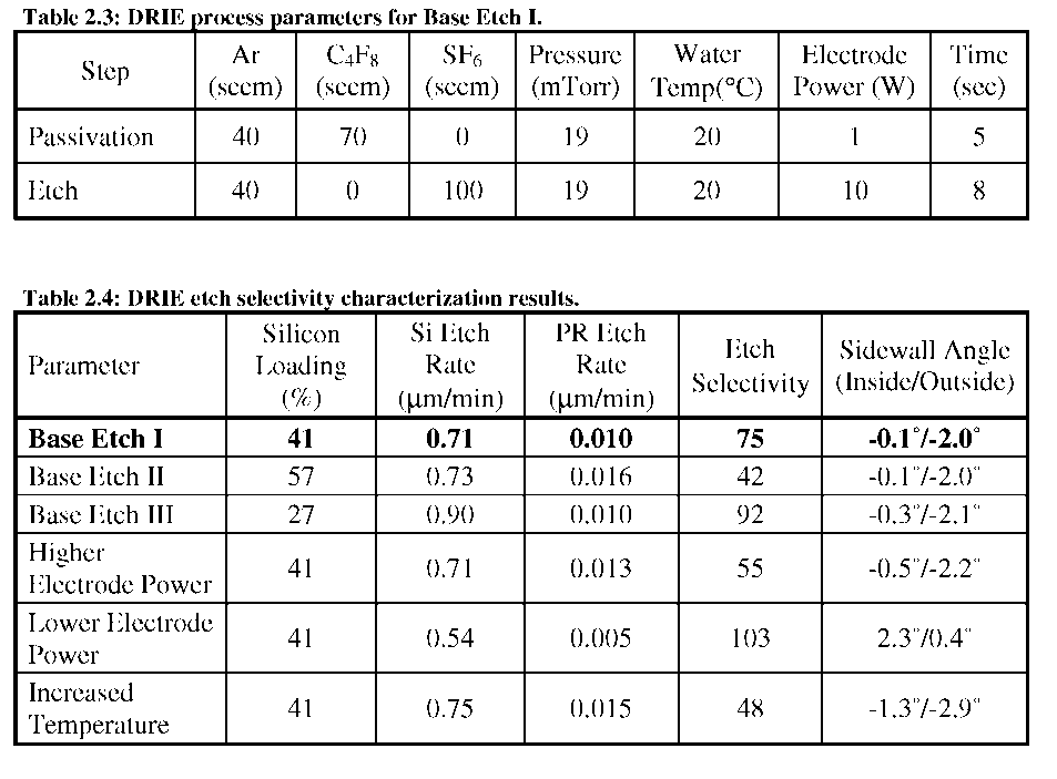
A number of experiments were carried out to assess the effect of changing various etch parameters on etch selectivity [16-18]. The starting etch recipe, termed Base Etch I, is shown in Table 2.3, and consists of separate passivation and etch steps within a time multiplexed cycle. Changes were made to Base Etch I regarding temperature, electrode power, and silicon loading because of anticipated effects on the etch selectivity. For example, increasing the electrode power will increase the rate at which the photoresist is sputtered from the surface due to ion bombardment, causing a corresponding decrease in etch selectivity. These results were presented in more detail in my Masters Thesis [18], but are summarized in Table 2.4.
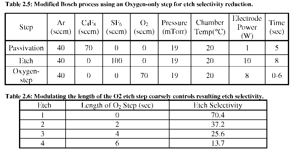
While the process changes described above may be applied in many cases, achieving extremely low etch selectivity (<20) may be difficult while maintaining other etch characteristics, such as sidewall profile. An alternative approach for coarse tuning of etch selectivity was also developed that uses an intermediate Oxygen-only step added to each passivation-etch cycle [16, 18], as shown in Table 2.5. Oxygen plasma steps are commonly used in MEMS and the IC industry for photoresist removal, and have minimal structural impact on silicon surfaces. But by adding a short Oxygen-only plasma step to each cycle, a thin layer of photoresist is removed during each cycle, effectively increasing the photoresist etch rate. The silicon etch rate should remain largely unaffected since the Oxygen plasma step is separate from the etching portion of the time- multiplexed cycle. By modulating the length of the Oxygen-only plasma step, the amount of photoresist removed during each cycle, and hence etch selectivity, can be coarsely controlled, as shown in Table 2.6.
The etch recipes and trends seen above are intended to serve as guidelines for etch development of specific structures. It must also be noted that while the selectivity can be changed over a wide range, there are nearly always tradeoffs with other etch parameters that may or may not be important, such as etch rate or sidewall angle/roughness. However, given the design flexibility afforded during the gray-scale lithography process, it is often possible to design for an etch selectivity range where other etch parameters are acceptable, and use the results above to fine-tune the process to achieve the appropriate final 3-D silicon structure. An example gray-scale wedge after being transferred into the silicon is shown in Figure 2.14.