

2. Synthesis of Synchronous fsm
Types of Tasks
Task 2.1
Design a circuit of a detector of input sequence specified by the variant of a task.
At giving the sequence to the input of Mealy FSM, signal "1" appears in its output. In all other cases - signal "0".
The variants of the tasks are presented in Table 6.
Table 6
Number of variant |
Input sequence |
1. |
11011, 10011 |
2. |
10001, 11001 |
3. |
010101, 000101 |
4. |
10010, 10011 |
5. |
001010, 101010 |
6. |
111011, 111010 |
7. |
000110, 100110 |
8 |
1110001, 101011 |
9 |
101011, 1110011 |
10 |
100001, 010111 |
Task 2.2
Design an FSM circuit, the input alphabet of which X = {A, B, C}, output alphabet of which {0,1,2}. FSM distinguishes input words and forms output words according to variant of the task presented in Table 7.
Table 7
Variant |
Input words |
1. |
ABCC – 1, BCAA – 2 |
2. |
ABBA – 1, ACBA – 2 |
3. |
CBAA – 1, CABCA – 2 |
4. |
ABCA – 1, CABC– 2 |
5. |
CCBAA – 1, CAB – 2 |
6. |
BBCA – 1, BAAC – 2 |
7. |
ABACB – 1, CAB – 2 |
8. |
CCAB – 1, AABC – 2 |
9. |
AAAB – 1, BCAB -2 |
10. |
AABBC – 1, BCC -2 |
11. |
ABAAA -1, BACB – 2 |
12. |
BBBC -1, ABC – 2 |
13. |
CCBC – 1, CCAB -2 |
14. |
ABBCA -1, BBA – 2 |
15. |
BCABC -1, CB – 2 |
16. |
BABC – 1, CAAC – 2 |
17. |
AABA – 1, CBCB – 2 |
18. |
CBAB – 1, BACB – 2 |
19. |
AABA – 1, BBA – 2 |
20. |
CCBC -1, AAB -2 |
21. |
AABC -1, BCAC – 2 |
22. |
ABCAB -1, CA -2 |
23. |
AACAB – 1, BBA -2 |
24. |
BBAB -1, CBA – 2 |
25. |
ACBA – 1, CBAAB -2 |
26 |
AABCC – 1, ABAB – 2 |
27 |
CBACB – 1, AABAB – 2 |
28 |
ACCBA – 1, ACCC- 2 |
29 |
BBCCA – 1, CBCA – 2 |
30 |
AABBC – 1, CCBCA – 2 |
Task 2.3.
Design Mealy FSM circuit, controlled by code lock, with one input X and two outputs Y1, Y2.
The output signal Y1 equals 1 in case X = 0, and the previous 5 steps in input X sequence, given by Table 10, from units and zero entered.
The output signal Y2 should equal 1 only when the current value X is correct from the viewpoint of FSM progress to the side of state at which the code lock is open.
The task variants are presented in Table 8.
Table 8
Number of variant |
Input sequence |
1. |
11011 |
2. |
01010 |
3. |
10101 |
4. |
00011 |
5. |
10011 |
6. |
10110 |
7. |
01001 |
8. |
11001 |
9. |
00100 |
10. |
01100 |
Task 2. 4.
Design a circuit of binary-coded decimal synchronous counter for different variants of coding decimal numbers. The counter accepts states from 0 to 9.
Table 10
Number of variant |
Binary-decimal code |
Counter direction |
1. |
Code with excess3 |
Up |
2. |
Code with excess 3 |
Down |
3. |
Code 2 out of 5 |
Up |
4. |
Code 2 out of 5 |
Down |
5. |
Biquinary code |
Up |
6. |
Biquinary code |
Down |
|
Codes with weights |
|
7. |
2 4 2 1 |
Up |
8. |
2 4 2 1 |
Down |
9. |
6 4 2 -1 |
Up |
10. |
6 4 2 -1 |
Down |
Task 2. 5.
Design Moore FSM circuit, the sequence of state changes of which is presented in Table 11.
In column “Output signal”, states are listed, in which the output of FSM is equal to one, in all other cases – “0”.
Table 11
Number of variant |
Sequence of states |
Output signal |
1. |
IN=1. 0®1®3®5®4®0 … IN=0. 0®5®4®3®1®0 … |
1 , 5 |
2.
|
IN=1. 0®2®7®1®4®0 … IN=0. 0®1®4®7®2®0 … |
2,7 |
3. |
IN=1. 0®5®2®1®3®0 … IN=0. 0®3®5®1®2®0 … |
1,2,5 |
4. |
IN=1. 0®3®6®5®2®0 … IN=0. 0®6®2®3®5®0 … |
3,5 |
5. |
IN=1. 0®1®6®2®5®0 … IN=0. 0®5®6®1®2®0 … |
2,6 |
6. |
IN=1. 0®5®4®1®3®0 … IN=0. 0®3®5®1®4®0 … |
1,3 |
7. |
IN=1. 0®2®1®7®6®0 … IN=0. 0®1®6®7®2®0 … |
2,7 |
8. |
IN=1. 0®2®7®1®4®0 … IN=0. 0®1®4®7®2®0 … |
1,4 |
Sequence of FSM synthesis
According to the given description, design a transition graph of FSM.
Choose the type of a flip-flop on which the FSM is implemented.
Assign FSM states.
Define excitation and output functions of FSM.
Minimize the obtained logic functions.
Design a circuit of FSM in AND, OR, NOT base.
Describe FSM in Verilog.
Simulate using VCS.
Synthesize the circuit with the help of Design Compiler. Use SAED EDK32/28nm technology library.
Specification using digital cells of SAED EDK90nm library.
Example (Part 1)
Design a circuit of the device that performs the conversion of input binary decimal code into output binary decimal code.
The weights of input code – 2421, the weight of output code – 8421.
The circuit of the code convertor has four inputs and four outputs.
Composition of the table of input and output codes.
Input and output codes are defined in the following way:
X = x1p1 + x2p2 +x3p3 + x4p4 = x12 + x24 +x32 + x41,
Y = y1p1’+y2p2’+y3p3’+y4p4’= y18+y24+y32+y41, where xi,yi{0,1}.
Table 12
Decimal digit |
Input code |
Output Code |
0 |
0 0 0 0 |
0 0 0 0 |
1 |
0 0 0 1 |
0 0 0 1 |
2 |
0 0 1 0 |
0 0 1 0 |
3 |
0 0 1 1 |
0 0 1 1 |
4 |
0 1 0 0 |
0 1 0 0 |
5 |
1 0 1 1 |
0 1 0 1 |
6 |
1 1 0 0 |
0 1 1 0 |
7 |
1 1 0 1 |
0 1 1 1 |
8 |
1 1 1 0 |
1 0 0 0 |
9 |
1 1 1 1 |
1 0 0 1 |
Composition of the table of implementing functions
Table 13
x1 x2 x3 x4 |
y1 y2 y3 y4 |
0 0 0 0 |
0 0 0 0 |
0 0 0 1 |
0 0 0 1 |
0 0 1 0 |
0 0 1 0 |
0 0 1 1 |
0 0 1 1 |
0 1 0 0 |
0 1 0 0 |
0 1 0 1 |
x x x x |
0 1 1 0 |
x x x x |
0 1 1 1 |
x x x x |
1 0 0 0 |
x x x x |
1 0 0 1 |
x x x x |
1 0 1 0 |
x x x x |
1 0 1 1 |
0 1 0 1 |
1 1 0 0 |
0 1 1 0 |
1 1 0 1 |
0 1 1 1 |
1 1 1 0 |
1 0 0 0 |
1 1 1 1 |
1 0 0 1 |
Boolean Functions Minimization
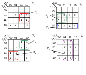
Fig.5. Minimization of functions using Karnaugh maps
y1= x2x3; y2=x2 ~x3 +x1~x2; y3 =~x1x3+x1~x3; y4=x4;
Design of circuits of the device on AND, OR, NOT basis
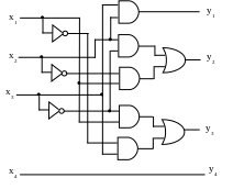
Fig. 6. The circuit using AND, OR, NOT gates
Design of circuits of the device on NAND basis
y

 1=
x2x3;
y2=(x2
~x3)(x1~x2);
y3
=(~x1x3
)(x1~x3)
;
1=
x2x3;
y2=(x2
~x3)(x1~x2);
y3
=(~x1x3
)(x1~x3)
;

Fig. 7. The circuit using NAND gates
Design of circuits of the device in basis NOR

y 1 = x2x3 = x2 +x3
P10 To
obtain y2
and y3
in POS it is possible to use Karnaugh maps for inverse functions
y2,y3.
To
obtain y2
and y3
in POS it is possible to use Karnaugh maps for inverse functions
y2,y3.
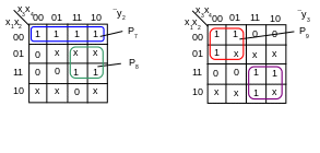
Fig. 8. Karnaugh maps for inverse functions
y2 = x1x2 + x2x3;


 y2
= x1x2
+ x2x3
= (x1+x2)
+ (x2
+x3)
;
y2
= x1x2
+ x2x3
= (x1+x2)
+ (x2
+x3)
;
y3 = x1x3 + x1x3;

y3 = x1x3 + x1x3 = (x1+x3) + (x1 +x3) ;
y4 = x4;
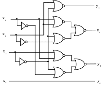
Fig. 9. The circuit using NOR gates
Definition of polynomials of implementing functions.
The polynomial form f(x1,x2,x3,x4) in general case:
f(x1,x2,x3,x4) = c0 c1x1 c2x2 c3x3 c4x4 c12x1x2 c13x1x3 . . . c1234 x1x2x3x4,
where ci{0,1}.
Find polynomial forms of y1,y2,y3,y4 functions, proceed from minimized form of these functions.
y1 = x2x3;
y2=x2 x3 +x1x2
Replace operation + by .
Then y2=x2 (1 x3) +x1 (1 x2) = x1 x2 x1x2 x2x3;
y3 = x1x3+x1x3 = x1 x3
y4=x4;
Implementation of the circuit of the code converter on the decoder
Decoder 4×16 is used to implement a function of 4 variables. But y1,y2,y3 depend on three variables only, therefore decoder 3×8 can be used.
Table 13
x1 x2 x3 |
y1 y2 y3 |
0 0 0 |
0 0 0 |
0 0 1 |
0 0 1 |
0 1 0 |
0 1 0 |
0 1 1 |
x x x |
1 0 0 |
x x x |
1 0 1 |
0 1 0 |
1 1 0 |
0 1 1 |
1 1 1 |
1 0 0 |
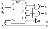
Fig.10. The circuit realization using decoder
Implementation of the circuit of the code converter on multiplexers
Multiplexers 4 – 1 are used to implement functions y1,y2,y3.
Y
= I0S1S0
+I1S1S0
+
I2S1S0
+ I3S1S0

Fig. 11. Logic symbol for multiplexer
y1 implementation
y1 = x2x3;
x2, x3 are entered to S1 and S0 inputs. Shannon cofactors y1 by x2,~x2, x3, ~x3 are entered to inputs I0, I1, I2, I3 .
I0= y1~x2,~x3 = 0;
I1 = y1~x2,x1 = 0;
I2 = y1x2,~x1 = 0;
I3 = y1x2,x1 = 1;
y2 implementation
x2, x3 are entered to S1 and S0 inputs. Shannon cofactors y2 by (~x3,~x2) – y2~x3,~x2 is entered to I0 input, cofactor y2~x3,x2 are given to I1 input, cofactor y2x3,~x2 are given to I2 input , cofactor y2x3,x2 are given to I3 input.
y2 = x2 ~x3 +x1~x2;
I0 = y2~x2,~x3 = x1;
I1 = y2~x2,x3 = x1;
I2 = y2x2,~x3 = 1;
I3 = y2x2,x3 = 0;
y3 implementation
x1,x3 are entered to S1 and S0 inputs. Shannon cofactors y3 by x1,~x1, x3, ~x3 are entered to inputs I0, I1, I2, I3 .
y3 =~x1x3+x1~x3;
I0 = y3~x1,~x3 = 0;
I1 = y3~x1,x3 = 1;
I2 = y3x1,~x3 = 1;
I3 = y3x1,x3 = 0;
The circuit is presented at Fig.9.
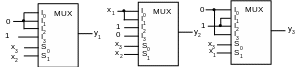
Fig.12. The circuit realization using multiplexers
Gate level description of the code converter circuit
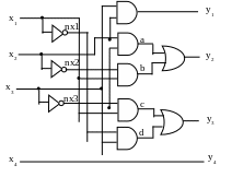
Fig.13. The circuit using AND, OR, NOT gates
module converter_decimal_numbers (x1,x2,x3,x4,y1,y2,y3,y4);
// port declarations
input x1,x2,x3,x4;
output y1,y2,y3,y4;
// internal wire declarations
wire nx1,nx2,nx3, a,b,c,d;
// create nx1,nx2,nx3;
not (nx1,x1);
not (nx2,x2);
not (nx3,x3);
// and gates instantiations
and (y1,x2,x3);
and (a,x2,nx3);
and (b,nx2,x1);
and (c,nx3,x1);
and (y1,nx1,x3);
//or gates instantiations
or (y2,a,b);
or (y3, c,d);
buf (y4,x4);
endmodule
Behavior Description of the code converter circuit
module converter_decimal_numbers (x,y);
input[1:4] x;
output reg [1:4] y;
always@(x)
case (x)
0: y=4b’0000;
1: y=4b’0001;
2: y=4b’0010;
3: y=4b’0011;
4: y=4b’0100;
5,6,7,8,9,1,10: y=4b’xxxx;
11: y=4b’0101;
12: y=4b’0110;
13: y=4b’0111;
14: y=4b’1000;
15: y=4b’1001;
endcase
endmodule
Synchronous FSM Synthesis (Part II)
Example
Design an FSM circuit, the input alphabet of which X = {A, B, C}, output alphabet of which {0,1,2}. FSM detects input words and forms output symbols in the following way:
If input word is BBCAB, Y=1.
If input word is BBC, Y=2. In all other cases Y=0.
1. Composition of Mealy FSM graph
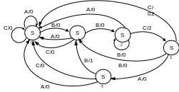
Fig. 14. State diagram of Mealy FSM
2. State minimization
Minimization task is in partitioning of set of states into classes of equivalent states and exchange of each class by one state.
1 = {X1,Y1,Z1}; X1={S0,S1,S3}; Y1={S2}; Z1={S4}
Si X |
A |
B |
C |
|
S0 |
S0/0 |
S1/0 |
S0/0 |
X1 |
S1 |
S0/0 |
S2/0 |
S0/0 |
X1 |
S2 |
S0/0 |
S2/0 |
S3/2 |
Y1 |
S3 |
S4/0 |
S1/0 |
S0/0 |
X1 |
S4 |
S0/0 |
S1/1 |
S0/0 |
Z1 |
Si X |
A |
B |
C |
|
S0 |
X1 |
X1 |
X1 |
X2 |
S1 |
X1 |
Y1 |
X1 |
Y2 |
S2 |
Z1 |
X1 |
X1 |
Z2 |
S3 |
- |
- |
- |
W2 |
S4 |
- |
- |
- |
K2 |
2 = {X2,Y2,Z2,W2,K2};
Each class contains only one state. Therefore FSM has no equivalent states.
The structure of Mealy FSM
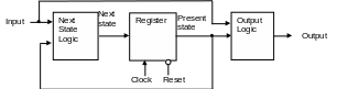
Fig. 15. Clocked synchronous Mealy FSM structure
3. Input and output signals coding
Coding input symbols
Input |
x1 x2 |
A |
0 0 |
B |
0 1 |
C |
1 0 |
Coding output symbols
Output |
y1 y |
“0” |
0 0 |
“1” |
0 1 |
“2” |
1 0 |
4. State assignment
Determine the number of state variables: choose the minimal number of state variables
n= log2 S where S – the number of states.
n=3.
The memory of FSM (register) is implemented using rising edge triggered JK flip-flops with asynchronous reset.
Symbols q1,q2,q3, are used for the present state variables.
The choice of state assignment is arbitrary in considering example.
State |
q1 q2 q3 |
S0 |
0 0 0 |
S1 |
0 0 1 |
S2 |
0 1 0 |
S3 |
0 1 1 |
S4 |
1 0 0 |
JK flip-flop excitation functions matrix
Transition |
J K |
0 - 0 |
0 x |
0 - 1 |
1 x |
1 - 0 |
x 1 |
1 - 1 |
x 0 |
5. Structural Table of Transitions
Present State q1 q2 q3 |
Input x1 x2 |
Next State q1 q2 q3 |
Output y1 y2 |
Excitation Functions J1 K1 J2 K2 J3 K3 |
|
S0 |
0 0 0 |
0 0 |
S0 0 0 0 |
0 0 |
0 x 0 x 0 x |
0 1 |
S1 0 0 1 |
0 0 |
0 x 0 x 1 x |
||
1 0 |
S0 0 0 0 |
0 0 |
0 x 0 x 0 x |
||
S1 |
0 0 1 |
0 0 |
S0 0 0 0 |
0 0 |
0 x 0 x x 1 |
0 1 |
S2 0 1 0 |
0 0 |
0 x 1 x x 0 |
||
1 0 |
S0 0 0 0 |
0 0 |
0 x 0 x x 1 |
||
S2 |
0 1 0 |
0 0 |
S0 0 0 0 |
0 0 |
0 x x 1 0 x |
0 1 |
S2 0 1 0 |
0 0 |
0 x x 0 0 x |
||
1 0 |
S3 0 1 1 |
1 0 |
0 x x 0 1 x |
||
S3 |
0 1 1 |
0 0 |
S4 1 0 0 |
0 0 |
1 x x 1 x 1 |
0 1 |
S1 0 0 1 |
0 0 |
0 x x 1 x 0 |
||
1 0 |
S0 0 0 0 |
0 0 |
0 x x 1 x 1 |
||
S4 |
1 0 0 |
0 0 |
S0 0 0 0 |
0 0 |
x 1 0 x 0 x |
0 1 |
S1 0 0 1 |
0 1 |
x 1 0 x 1 x |
||
1 0 |
S0 0 0 0 |
0 0 |
x 1 0 x 0 x |
||