

Digital Signal Processing. The Scientist and Engineers Guide. Steven W. Smith
.pdf
|
|
|
|
|
Chapter 28Digital Signal Processors |
|
|
|
507 |
|||||||
MEMORY |
STORED |
|
|
|
|
|
MEMORY |
STORED |
|
|
|
|
|
|
||
ADDRESS |
VALUE |
|
|
|
|
|
ADDRESS |
VALUE |
|
|
|
|
|
|
||
20040 |
|
|
|
|
|
|
|
20040 |
|
|
|
|
|
|
|
|
|
|
|
|
|
|
|
|
|
|
|
|
|
|
|
||
20041 |
-0.225767 |
|
|
x[n-3] |
|
|
20041 |
-0.225767 |
|
|
x[n-4] |
|
|
|
||
|
|
|
|
|
|
|
|
|||||||||
20042 |
-0.269847 |
|
|
x[n-2] |
|
|
20042 |
-0.269847 |
|
|
x[n-3] |
|
|
|
||
|
|
|
|
|
|
|
|
|||||||||
|
|
|
|
|
x[n-1] |
|
|
|
|
|
|
|
x[n-2] |
|
|
|
20043 |
-0.228918 |
|
|
|
|
20043 |
-0.228918 |
|
|
|
|
|
||||
|
|
|
|
|
|
|
|
|||||||||
|
|
|
|
|
x[n] |
newest sample |
|
|
|
|
|
x[n-1] |
|
|
|
|
20044 |
-0.113940 |
|
|
20044 |
-0.113940 |
|
|
|
|
|
||||||
|
|
|
|
|
|
|||||||||||
20045 |
|
|
|
|
x[n-7] |
oldest sample |
20045 |
|
|
|
|
x[n] |
newest sample |
|
||
-0.048679 |
|
|
-0.062222 |
|
|
|
||||||||||
|
|
|
||||||||||||||
|
|
|
|
|
x[n-6] |
|
|
|
|
|
|
|
x[n-7] |
oldest sample |
|
|
20046 |
-0.222977 |
|
|
|
|
20046 |
-0.222977 |
|
|
|
||||||
|
|
|
|
|||||||||||||
|
|
|
|
|
||||||||||||
|
|
|
|
|
x[n-5] |
|
|
|
|
|
|
|
x[n-6] |
|
|
|
20047 |
-0.371370 |
|
|
|
|
20047 |
-0.371370 |
|
|
|
|
|
||||
|
|
|
|
|
|
|
|
|
||||||||
|
|
|
|
|
|
|
|
|||||||||
20048 |
-0.462791 |
|
|
x[n-4] |
|
|
20048 |
-0.462791 |
|
|
x[n-5] |
|
|
|
||
|
|
|
|
|
|
|
|
|||||||||
20049 |
|
|
|
|
|
|
|
20049 |
|
|
|
|
|
|
|
|
|
|
|
|
|
|
|
|
|
|
|
|
|
|
|
||
|
|
|
|
|
|
|
|
|
|
|
|
|
|
|
||
a. |
Circular buffer at some instant |
b. Circular buffer after next sample |
||||||||||||||
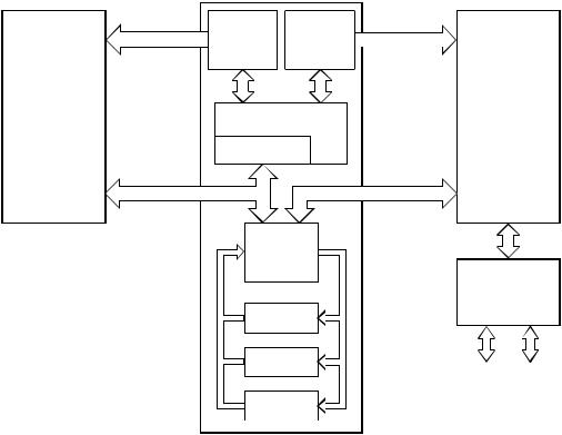
FIGURE 28-3
Circular buffer operation. Circular buffers are used to store the most recent values of a continually updated signal. This illustration shows how an eight sample circular buffer might appear at some instant in time (a), and how it would appear one sample later (b).
of samples, perform the algorithm, and output a group of samples. This is the world of Digital Signal Processors.
Now look back at Fig. 28-2 and imagine that this is an FIR filter being implemented in real-time. To calculate the output sample, we must have access to a certain number of the most recent samples from the input. For example, suppose we use eight coefficients in this filter, a0, a1, þ a7 . This means we must know the value of the eight most recent samples from the input signal, x[n], x[n& 1], þ x[n& 7] . These eight samples must be stored in memory and continually updated as new samples are acquired. What is the best way to manage these stored samples? The answer is circular buffering.
Figure 28-3 illustrates an eight sample circular buffer. We have placed this circular buffer in eight consecutive memory locations, 20041 to 20048. Figure
(a) shows how the eight samples from the input might be stored at one particular instant in time, while (b) shows the changes after the next sample is acquired. The idea of circular buffering is that the end of this linear array is connected to its beginning; memory location 20041 is viewed as being next to 20048, just as 20044 is next to 20045. You keep track of the array by a pointer (a variable whose value is an address) that indicates where the most recent sample resides. For instance, in (a) the pointer contains the address 20044, while in (b) it contains 20045. When a new sample is acquired, it replaces the oldest sample in the array, and the pointer is moved one address ahead. Circular buffers are efficient because only one value needs to be changed when a new sample is acquired.
Four parameters are needed to manage a circular buffer. First, there must be a pointer that indicates the start of the circular buffer in memory (in this example, 20041). Second, there must be a pointer indicating the end of the

Chapter 28Digital Signal Processors |
509 |
The goal is to make these steps execute quickly. Since steps 6-12 will be repeated many times (once for each coefficient in the filter), special attention must be given to these operations. Traditional microprocessors must generally carry out these 14 steps in serial (one after another), while DSPs are designed to perform them in parallel. In some cases, all of the operations within the loop (steps 6-12) can be completed in a single clock cycle. Let's look at the internal architecture that allows this magnificent performance.
Architecture of the Digital Signal Processor
One of the biggest bottlenecks in executing DSP algorithms is transferring information to and from memory. This includes data, such as samples from the input signal and the filter coefficients, as well as program instructions, the binary codes that go into the program sequencer. For example, suppose we need to multiply two numbers that reside somewhere in memory. To do this, we must fetch three binary values from memory, the numbers to be multiplied, plus the program instruction describing what to do.
Figure 28-4a shows how this seemingly simple task is done in a traditional microprocessor. This is often called a Von Neumann architecture, after the brilliant American mathematician John Von Neumann (1903-1957). Von Neumann guided the mathematics of many important discoveries of the early twentieth century. His many achievements include: developing the concept of a stored program computer, formalizing the mathematics of quantum mechanics, and work on the atomic bomb. If it was new and exciting, Von Neumann was there!
As shown in (a), a Von Neumann architecture contains a single memory and a single bus for transferring data into and out of the central processing unit (CPU). Multiplying two numbers requires at least three clock cycles, one to transfer each of the three numbers over the bus from the memory to the CPU. We don't count the time to transfer the result back to memory, because we assume that it remains in the CPU for additional manipulation (such as the sum of products in an FIR filter). The Von Neumann design is quite satisfactory when you are content to execute all of the required tasks in serial. In fact, most computers today are of the Von Neumann design. We only need other architectures when very fast processing is required, and we are willing to pay the price of increased complexity.
This leads us to the Harvard architecture, shown in (b). This is named for the work done at Harvard University in the 1940s under the leadership of Howard Aiken (1900-1973). As shown in this illustration, Aiken insisted on separate memories for data and program instructions, with separate buses for each. Since the buses operate independently, program instructions and data can be fetched at the same time, improving the speed over the single bus design. Most present day DSPs use this dual bus architecture.
Figure (c) illustrates the next level of sophistication, the Super Harvard Architecture. This term was coined by Analog Devices to describe the
510 |
The Scientist and Engineer's Guide to Digital Signal Processing |
internal operation of their ADSP-2106x and new ADSP-211xx families of Digital Signal Processors. These are called SHARC® DSPs, a contraction of the longer term, Super Harvard ARChitecture. The idea is to build upon the Harvard architecture by adding features to improve the throughput. While the SHARC DSPs are optimized in dozens of ways, two areas are important enough to be included in Fig. 28-4c: an instruction cache, and an I/O controller.
First, let's look at how the instruction cache improves the performance of the Harvard architecture. A handicap of the basic Harvard design is that the data memory bus is busier than the program memory bus. When two numbers are multiplied, two binary values (the numbers) must be passed over the data memory bus, while only one binary value (the program instruction) is passed over the program memory bus. To improve upon this situation, we start by relocating part of the "data" to program memory. For instance, we might place the filter coefficients in program memory, while keeping the input signal in data memory. (This relocated data is called "secondary data" in the illustration). At first glance, this doesn't seem to help the situation; now we must transfer one value over the data memory bus (the input signal sample), but two values over the program memory bus (the program instruction and the coefficient). In fact, if we were executing random instructions, this situation would be no better at all.
However, DSP algorithms generally spend most of their execution time in loops, such as instructions 6-12 of Table 28-1. This means that the same set of program instructions will continually pass from program memory to the CPU. The Super Harvard architecture takes advantage of this situation by including an instruction cache in the CPU. This is a small memory that contains about 32 of the most recent program instructions. The first time through a loop, the program instructions must be passed over the program memory bus. This results in slower operation because of the conflict with the coefficients that must also be fetched along this path. However, on additional executions of the loop, the program instructions can be pulled from the instruction cache. This means that all of the memory to CPU information transfers can be accomplished in a single cycle: the sample from the input signal comes over the data memory bus, the coefficient comes over the program memory bus, and the program instruction comes from the instruction cache. In the jargon of the field, this efficient transfer of data is called a high memoryaccess bandwidth.
Figure 28-5 presents a more detailed view of the SHARC architecture, showing the I/O controller connected to data memory. This is how the signals enter and exit the system. For instance, the SHARC DSPs provides both serial and parallel communications ports. These are extremely high speed connections. For example, at a 40 MHz clock speed, there are two serial ports that operate at 40 Mbits/second each, while six parallel ports each provide a 40 Mbytes/second data transfer. When all six parallel ports are used together, the data transfer rate is an incredible 240 Mbytes/second.


512 |
The Scientist and Engineer's Guide to Digital Signal Processing |
Now let's look inside the CPU. At the top of the diagram are two blocks labeled Data Address Generator (DAG), one for each of the two memories. These control the addresses sent to the program and data memories, specifying where the information is to be read from or written to. In simpler microprocessors this task is handled as an inherent part of the program sequencer, and is quite transparent to the programmer. However, DSPs are designed to operate with circular buffers, and benefit from the extra hardware to manage them efficiently. This avoids needing to use precious CPU clock cycles to keep track of how the data are stored. For instance, in the SHARC DSPs, each of the two DAGs can control eight circular buffers. This means that each DAG holds 32 variables (4 per buffer), plus the required logic.
Why so many circular buffers? Some DSP algorithms are best carried out in stages. For instance, IIR filters are more stable if implemented as a cascade of biquads (a stage containing two poles and up to two zeros). Multiple stages require multiple circular buffers for the fastest operation. The DAGs in the SHARC DSPs are also designed to efficiently carry out the Fast Fourier transform. In this mode, the DAGs are configured to generate bit-reversed addresses into the circular buffers, a necessary part of the FFT algorithm. In addition, an abundance of circular buffers greatly simplifies DSP code generationboth for the human programmer as well as high-level language compilers, such as C.
The data register section of the CPU is used in the same way as in traditional microprocessors. In the ADSP-2106x SHARC DSPs, there are 16 general purpose registers of 40 bits each. These can hold intermediate calculations, prepare data for the math processor, serve as a buffer for data transfer, hold flags for program control, and so on. If needed, these registers can also be used to control loops and counters; however, the SHARC DSPs have extra hardware registers to carry out many of these functions.
The math processing is broken into three sections, a multiplier, an arithmetic logic unit (ALU), and a barrel shifter. The multiplier takes the values from two registers, multiplies them, and places the result into another register. The ALU performs addition, subtraction, absolute value, logical operations (AND, OR, XOR, NOT), conversion between fixed and floating point formats, and similar functions. Elementary binary operations are carried out by the barrel shifter, such as shifting, rotating, extracting and depositing segments, and so on. A powerful feature of the SHARC family is that the multiplier and the ALU can be accessed in parallel. In a single clock cycle, data from registers 0-7 can be passed to the multiplier, data from registers 8-15 can be passed to the ALU, and the two results returned to any of the 16 registers.
There are also many important features of the SHARC family architecture that aren't shown in this simplified illustration. For instance, an 80 bit accumulator is built into the multiplier to reduce the round-off error associated with multiple fixed-point math operations. Another interesting
Chapter 28Digital Signal Processors |
513 |
|||||||
|
|
|
|
|
|
|
|
|
|
|
PM Data |
|
|
DM Data |
|
|
|
PM address bus |
|
Address |
|
|
Address |
DM address bus |
|
|
|
Generator |
|
|
Generator |
|
|
||
Program |
|
|
|
|
|
|
|
Data |
|
|
|
|
|
|
|
||
Memory |
|
|
|
|
|
|
|
Memory |
|
Program Sequencer |
|
|
|||||
instructions and |
|
|
|
|||||
|
|
|
|
|
|
|
data only |
|
secondary data |
|
Instruction |
|
|
|
|||
|
|
|
|
|
||||
|
|
Cache |
|
|
|
|
||
PM data bus |
|
|
|
|
|
|
DM data bus |
|
Data
Registers
|
I/O Controller |
|
(DMA) |
Muliplier |
|
|
|
|
|
ALU |
High speed I/O |
|
|
|
|
|
(serial, parallel, |
Shifter |
ADC, DAC, etc.) |
|
|
|
|
FIGURE 28-5
Typical DSP architecture. Digital Signal Processors are designed to implement tasks in parallel. This simplified diagram is of the Analog Devices SHARC DSP. Compare this architecture with the tasks needed to implement an FIR filter, as listed in Table 28-1. All of the steps within the loop can be executed in a single clock cycle.
feature is the use of shadow registers for all the CPU's key registers. These are duplicate registers that can be switched with their counterparts in a single clock cycle. They are used for fast context switching, the ability to handle interrupts quickly. When an interrupt occurs in traditional microprocessors, all the internal data must be saved before the interrupt can be handled. This usually involves pushing all of the occupied registers onto the stack, one at a time. In comparison, an interrupt in the SHARC family is handled by moving the internal data into the shadow registers in a single clock cycle. When the interrupt routine is completed, the registers are just as quickly restored. This feature allows step 4 on our list (managing the sample-ready interrupt) to be handled very quickly and efficiently.
Now we come to the critical performance of the architecture, how many of the operations within the loop (steps 6-12 of Table 28-1) can be carried out at the same time. Because of its highly parallel nature, the SHARC DSP can simultaneously carry out all of these tasks. Specifically, within a single clock cycle, it can perform a multiply (step 11), an addition (step 12), two data moves (steps 7 and 9), update two circular buffer pointers (steps 8 and 10), and
514 |
The Scientist and Engineer's Guide to Digital Signal Processing |
control the loop (step 6). There will be extra clock cycles associated with beginning and ending the loop (steps 3, 4, 5 and 13, plus moving initial values into place); however, these tasks are also handled very efficiently. If the loop is executed more than a few times, this overhead will be negligible. As an example, suppose you write an efficient FIR filter program using 100 coefficients. You can expect it to require about 105 to 110 clock cycles per sample to execute (i.e., 100 coefficient loops plus overhead). This is very impressive; a traditional microprocessor requires many thousands of clock cycles for this algorithm.
Fixed versus Floating Point
Digital Signal Processing can be divided into two categories, fixed point and floating point. These refer to the format used to store and manipulate numbers within the devices. Fixed point DSPs usually represent each number with a minimum of 16 bits, although a different length can be used. For instance, Motorola manufactures a family of fixed point DSPs that use 24 bits. There are four common ways that these 216 ' 65,536 possible bit patterns can represent a number. In unsigned integer, the stored number can take on any integer value from 0 to 65,535. Similarly, signed integer uses two's complement to make the range include negative numbers, from -32,768 to 32,767. With unsigned fraction notation, the 65,536 levels are spread uniformly between 0 and 1. Lastly, the signed fraction format allows negative numbers, equally spaced between -1 and 1.
In comparison, floating point DSPs typically use a minimum of 32 bits to store each value. This results in many more bit patterns than for fixed point, 232 ' 4,294,967,296 to be exact. A key feature of floating point notation is that the represented numbers are not uniformly spaced. In the most common format (ANSI/IEEE Std. 754-1985), the largest and smallest numbers are
± 3.4 × 1038 and ± 1.2 × 10& 38 , respectively. The represented values are unequally spaced between these two extremes, such that the gap between any two numbers is about ten-million times smaller than the value of the numbers.
This is important because it places large gaps between large numbers, but small gaps between small numbers. Floating point notation is discussed in more detail in Chapter 4.
All floating point DSPs can also handle fixed point numbers, a necessity to implement counters, loops, and signals coming from the ADC and going to the DAC. However, this doesn't mean that fixed point math will be carried out as quickly as the floating point operations; it depends on the internal architecture. For instance, the SHARC DSPs are optimized for both floating point and fixed point operations, and executes them with equal efficiency. For this reason, the SHARC devices are often referred to as "32-bit DSPs," rather than just "Floating Point."
Figure 28-6 illustrates the primary trade-offs between fixed and floating point DSPs. In Chapter 3 we stressed that fixed point arithmetic is much
516 |
The Scientist and Engineer's Guide to Digital Signal Processing |
want to store the number 1000, the gap between numbers is only one onethousandth of the value.
Noise in signals is usually represented by its standard deviation. This was discussed in detail in Chapter 2. For here, the important fact is that the standard deviation of this quantization noise is about one-third of the gap size. This means that the signal-to-noise ratio for storing a floating point number is about 30 million to one, while for a fixed point number it is only about ten-thousand to one. In other words, floating point has roughly 3,000 times less quantization noise than fixed point.
This brings up an important way that DSPs are different from traditional microprocessors. Suppose we implement an FIR filter in fixed point. To do this, we loop through each coefficient, multiply it by the appropriate sample from the input signal, and add the product to an accumulator. Here's the problem. In traditional microprocessors, this accumulator is just another 16 bit fixed point variable. To avoid overflow, we need to scale the values being added, and will correspondingly add quantization noise on each step. In the worst case, this quantization noise will simply add, greatly lowering the signal- to-noise ratio of the system. For instance, in a 500 coefficient FIR filter, the noise on each output sample may be 500 times the noise on each input sample. The signal-to-noise ratio of ten-thousand to one has dropped to a ghastly twenty to one. Although this is an extreme case, it illustrates the main point: when many operations are carried out on each sample, it's bad, really bad. See Chapter 3 for more details.
DSPs handle this problem by using an extended precision accumulator. This is a special register that has 2-3 times as many bits as the other memory locations. For example, in a 16 bit DSP it may have 32 to 40 bits, while in the SHARC DSPs it contains 80 bits for fixed point use. This extended range virtually eliminates round-off noise while the accumulation is in progress. The only round-off error suffered is when the accumulator is scaled and stored in the 16 bit memory. This strategy works very well, although it does limit how some algorithms must be carried out. In comparison, floating point has such low quantization noise that these techniques are usually not necessary.
In addition to having lower quantization noise, floating point systems are also easier to develop algorithms for. Most DSP techniques are based on repeated multiplications and additions. In fixed point, the possibility of an overflow or underflow needs to be considered after each operation. The programmer needs to continually understand the amplitude of the numbers, how the quantization errors are accumulating, and what scaling needs to take place. In comparison, these issues do not arise in floating point; the numbers take care of themselves (except in rare cases).
To give you a better understanding of this issue, Fig. 28-7 shows a table from the SHARC user manual. This describes the ways that multiplication can be carried out for both fixed and floating point formats. First, look at how floating point numbers can be multiplied; there is only one way! That