

Philips Semiconductors |
Product specification |
|
|
48 × 84 pixels matrix LCD controller/driver |
PCD8544 |
|
|
8 INSTRUCTIONS
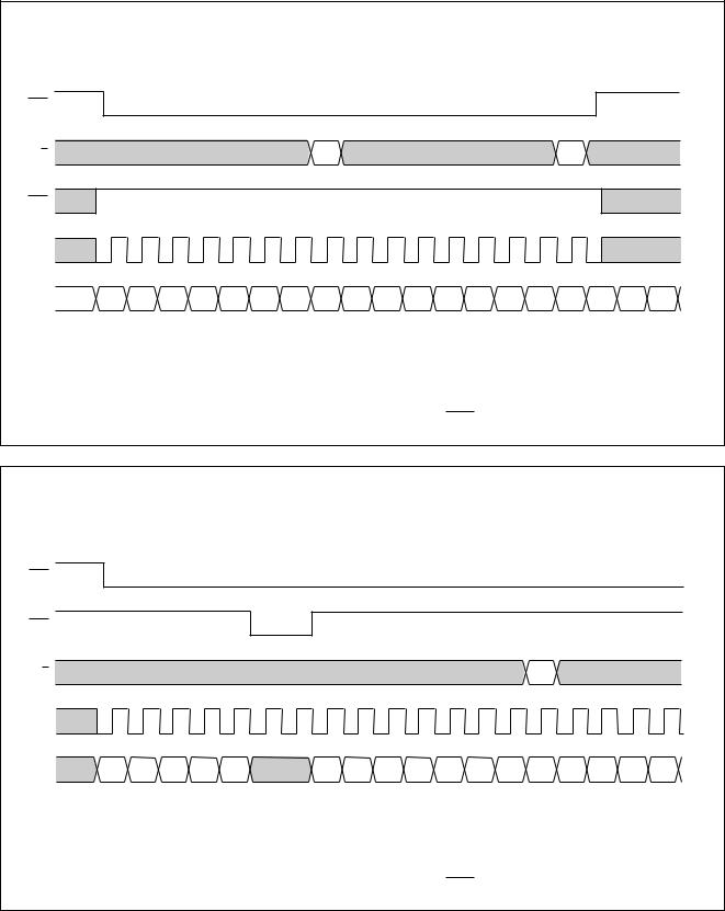
The instruction format is divided into two modes: If D/C (mode select) is set LOW, the current byte is interpreted as command byte (see Table 1). Figure 8 shows an example of a serial data stream for initializing the chip. If D/C is set HIGH, the following bytes are stored in the display data RAM. After every data byte, the address counter is incremented automatically.
The level of the D/C signal is read during the last bit of data byte.
Each instruction can be sent in any order to the PCD8544. The MSB of a byte is transmitted first. Figure 9 shows one possible command stream, used to set up the LCD driver.
The serial interface is initialized when SCE is HIGH. In this state, SCLK clock pulses have no effect and no power is consumed by the serial interface. A negative edge on SCE enables the serial interface and indicates the start of a data transmission.
MSB (DB7) |
|
|
LSB (DB0) |
||||||||||||
|
|
|
|
|
|
|
|
|
|
|
|
|
|
|
|
|
|
|
data |
|
|
|
|
|
|
data |
|||||
|
|
|
|
|
|
|
|
|
|
|
|
|
|
|
|
MGL666
Fig.8 General format of data stream.
|
|
|
|
|
|
|
|
|
|
|
|
|
|
|
|
|
|
|
|
|
|
|
|
|
|
|
|
|
|
|
|
function set (H = 1) |
|
|
bias system |
|
|
set VOP |
|
|
|
temperature control |
|||||||||||||||||||||
|
|
|
|
|
|
|
|
|
|
|
|
|
|
|
|
|
|
|
|
|
|
|
|
|
|
|
|
|
|
|
|
|
|
|
|
|
|
|
|
|
|
|
|
|
|
|
|
|
|
|
|
|
|
|
|
|
|
|
|
|
|
|
|
function set (H = 0) |
|
display control |
|
|
Y address |
|
|
X address |
|||||||||||||||||||||||
|
|
|
|
|
|
|
|
|
|
|
|
|
|
|
|
|
|
|
|
|
|
|
|
|
|
|
|
|
|
|
|
|
|
|
|
|
|
|
|
|
|
|
|
|
|
|
|
|
|
|
|
|
|
|
|
|
|
|
|
|
|
|
|
MGL642
Fig.9 Serial data stream, example.
Figures 10 and 11 show the serial bus protocol.
∙When SCE is HIGH, SCLK clock signals are ignored; during the HIGH time of SCE, the serial interface is initialized (see Fig.12)
∙SDIN is sampled at the positive edge of SCLK
∙D/C indicates whether the byte is a command (D/C = 0) or RAM data (D/C = 1); it is read with the eighth SCLK pulse
∙If SCE stays LOW after the last bit of a command/data byte, the serial interface expects bit 7 of the next byte at the next positive edge of SCLK (see Fig.12)
∙A reset pulse with RES interrupts the transmission. No data is written into the RAM. The registers are cleared. If SCE is LOW after the positive edge of RES, the serial interface is ready to receive bit 7 of a command/data byte (see Fig.13).
1999 Apr 12 |
11 |

Philips Semiconductors |
Product specification |
|
|
48 × 84 pixels matrix LCD controller/driver |
PCD8544 |
|
|
SCE
D/C
SCLK
SDIN |
DB7 |
DB6 |
DB5 |
DB4 |
DB3 |
DB2 |
DB1 |
DB0 |
MGL630
Fig.10 Serial bus protocol - transmission of one byte.
SCE |
|
D/C |
|
SCLK |
|
SDIN |
DB7 DB6 DB5 DB4 DB3 DB2 DB1 DB0 DB7 DB6 DB5 DB4 DB3 DB2 DB1 DB0 DB7 DB6 DB5 |
|
MGL631 |
Fig.11 Serial bus protocol - transmission of several bytes.
1999 Apr 12 |
12 |
Philips Semiconductors |
Product specification |
|
|
48 × 84 pixels matrix LCD controller/driver |
PCD8544 |
|
|
SCE |
|
D/C |
|
RES |
|
SCLK |
|
SDIN |
DB7 DB6 DB5 DB4 DB3 DB2 DB1 DB0 DB7 DB6 DB5 DB4 DB3 DB2 DB1 DB0 DB7 DB6 DB5 |
|
MGL632 |
Fig.12 Serial bus reset function (SCE).
SCE |
|
|
RES |
|
|
D/C |
|
|
SCLK |
|
|
SDIN |
DB7 DB6 DB5 DB4 DB3 |
DB7 DB6 DB5 DB4 DB3 DB2 DB1 DB0 DB7 DB6 DB5 DB4 |
|
|
MGL633 |
Fig.13 Serial bus reset function (RES).
1999 Apr 12 |
13 |

Philips Semiconductors |
|
|
|
|
|
|
|
|
Product specification |
||||
|
|
|
|
|
|
|
|
|
|
|
|
|
|
48 × 84 pixels matrix LCD controller/driver |
|
|
PCD8544 |
||||||||||
|
|
|
|
|
|
|
|
|
|
|
|
|
|
Table 1 Instruction set |
|
|
|
|
|
|
|
|
|
||||
|
|
|
|
|
|
|
|
|
|
|
|
|
|
|
|
|
|
|
|
COMMAND BYTE |
|
|
|
||||
INSTRUCTION |
D/C |
|
|
|
|
DESCRIPTION |
|||||||
|
|
|
|
|
|
|
|
||||||
DB7 |
DB6 |
DB5 |
DB4 |
DB3 |
DB2 |
DB1 |
DB0 |
||||||
|
|
|
|
|
|||||||||
|
|
|
|
|
|
|
|
|
|
|
|
|
|
(H = 0 or 1) |
|
|
|
|
|
|
|
|
|
|
|
|
|
|
|
|
|
|
|
|
|
|
|
|
|
|
|
NOP |
0 |
|
|
0 |
0 |
0 |
0 |
0 |
0 |
0 |
0 |
no operation |
|
|
|
|
|
|
|
|
|
|
|
|
|
|
|
Function set |
0 |
|
|
0 |
0 |
1 |
0 |
0 |
PD |
V |
H |
power down control; entry |
|
|
|
|
|
|
|
|
|
|
|
|
|
mode; extended instruction set |
|
|
|
|
|
|
|
|
|
|
|
|
|
control (H) |
|
|
|
|
|
|
|
|
|
|
|
|
|
|
|
Write data |
1 |
|
|
D7 |
D6 |
D5 |
D4 |
D3 |
D2 |
D1 |
D0 |
writes data to display RAM |
|
(H = 0) |
|
|
|
|
|
|
|
|
|
|
|
|
|
|
|
|
|
|
|
|
|
|
|
|
|
|
|
Reserved |
0 |
|
|
0 |
0 |
0 |
0 |
0 |
1 |
X |
X |
do not use |
|
|
|
|
|
|
|
|
|
|
|
|
|
|
|
Display control |
0 |
|
|
0 |
0 |
0 |
0 |
1 |
D |
0 |
E |
sets display configuration |
|
|
|
|
|
|
|
|
|
|
|
|
|
|
|
Reserved |
0 |
|
|
0 |
0 |
0 |
1 |
X |
X |
X |
X |
do not use |
|
|
|
|
|
|
|
|
|
|
|
|
|
|
|
Set Y address of |
0 |
|
|
0 |
1 |
0 |
0 |
0 |
Y2 |
Y1 |
Y0 |
sets Y-address of RAM; |
|
RAM |
|
|
|
|
|
|
|
|
|
|
|
0 ≤ Y ≤ 5 |
|
|
|
|
|
|
|
|
|
|
|
|
|
|
|
Set X address of |
0 |
|
|
1 |
X6 |
X5 |
X4 |
X3 |
X2 |
X1 |
X0 |
sets X-address part of RAM; |
|
RAM |
|
|
|
|
|
|
|
|
|
|
|
0 ≤ X ≤ 83 |
|
|
|
|
|
|
|
|
|
|
|
|
|
|
|
(H = 1) |
|
|
|
|
|
|
|
|
|
|
|
|
|
|
|
|
|
|
|
|
|
|
|
|
|
|
|
Reserved |
0 |
|
|
0 |
0 |
0 |
0 |
0 |
0 |
0 |
1 |
do not use |
|
|
|
|
|
|
|
|
|
|
|
|
|
|
|
|
0 |
|
|
0 |
0 |
0 |
0 |
0 |
0 |
1 |
X |
do not use |
|
|
|
|
|
|
|
|
|
|
|
|
|
|
|
Temperature |
0 |
|
|
0 |
0 |
0 |
0 |
0 |
1 |
TC1 |
TC0 |
set Temperature Coefficient |
|
control |
|
|
|
|
|
|
|
|
|
|
|
(TCx) |
|
Reserved |
0 |
|
|
0 |
0 |
0 |
0 |
1 |
X |
X |
X |
do not use |
|
|
|
|
|
|
|
|
|
|
|
|
|
|
|
Bias system |
0 |
|
|
0 |
0 |
0 |
1 |
0 |
BS2 |
BS1 |
BS0 |
set Bias System (BSx) |
|
Reserved |
0 |
|
|
0 |
1 |
X |
X |
X |
X |
X |
X |
do not use |
|
|
|
|
|
|
|
|
|
|
|
|
|
|
|
Set VOP |
0 |
|
|
1 |
VOP6 |
VOP5 |
VOP4 |
VOP3 |
VOP2 |
VOP1 |
VOP0 |
write VOP to register |
|
Table 2 Explanations of symbols in Table 1 |
|
|
|
|
|
|
|||||||
|
|
|
|
|
|
|
|
|
|
|
|
|
|
BIT |
|
|
|
|
|
0 |
|
|
|
|
|
1 |
|
|
|
|
|
|
|
|
|
||||||
PD |
chip is active |
|
|
|
|
|
chip is in Power-down mode |
||||||
|
|
|
|
|
|
|
|||||||
V |
horizontal addressing |
|
|
|
|
vertical addressing |
|||||||
|
|
|
|
|
|
||||||||
H |
use basic instruction set |
|
|
|
use extended instruction set |
||||||||
|
|
|
|
|
|
|
|
|
|
|
|
|
|
D and E |
|
|
|
|
|
|
|
|
|
|
|
|
|
00 |
display blank |
|
|
|
|
|
|
|
|
||||
10 |
normal mode |
|
|
|
|
|
|
|
|
||||
01 |
all display segments on |
|
|
|
|
|
|
||||||
11 |
inverse video mode |
|
|
|
|
|
|
|
|||||
|
|
|
|
|
|
|
|
|
|
|
|
|
|
TC1 and TC0 |
|
|
|
|
|
|
|
|
|
|
|
|
|
00 |
VLCD temperature coefficient 0 |
|
|
|
|
|
|||||||
01 |
VLCD temperature coefficient 1 |
|
|
|
|
|
|||||||
10 |
VLCD temperature coefficient 2 |
|
|
|
|
|
|||||||
11 |
VLCD temperature coefficient 3 |
|
|
|
|
|
|||||||
1999 Apr 12 |
14 |