

3D Simulators and Wa¨eguide Bandpass Filter Design |
487 |
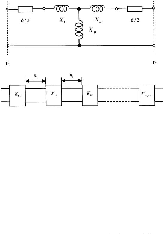
Figure 3. Lumped element equivalent network of a discontinuity.
circular cylindrical for the posts.. Also, the equations for K inverters presented in the preceding text have limitations; those do not take into consideration the frequency dependence of the waveguide discontinuities.
III. THE FULL-WAVE THREE-DIMENSIONAL MODELING BASED APPROACHED WITH DISTRIBUTED ELEMENT K-INVERTERS OF LEVY AND RHODES
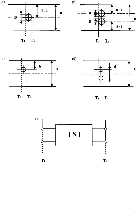
A viable option is the full electromagnetic modeling of an off-centered round post discontinuity in a rectangular waveguide. A number of papers have appeared in the literature that deal with such analysis w12x. At the same time, today, there exist a number of very accurate full electromagnetic analysis based commercially available software which can be used to generate the design model for the K inverters for the filter configuration shown in Figure 1. The transmission line matrix analysis based software MICROSTRIPE w4x was used to develop the model for the K inverters for the round rod discontinuities shown in Figure 4. We will also calculate the required K-inverter values for our filters using the distributed element prototype network by Levy w13x
and Rhodes w14x. According to w13x and w14x the required K-inverter values for a filter are obtained as described in the following text:
1. The order of the filter, N, will give the number of resonators and N q 1 will be the number of rod couplers needed to meet the design specifications. N is determined from the ripple bandwidth D f, the isolation bandwidth D fi , the passband return loss Lr , and the stop band isolation Ls of the filter using the following equation for a Chebyshev type response. The filter order is given by w14x. Thus,
|
Ls |
q Lr |
q 6 |
||
N G |
|
|
|
|
, 8a. |
|
|
|
|
||
|
20 log g q 'g 2 y 1 / |
||||
where g is the ratio D firD f.
2. The midband guide wavelength lgo is determined by solving w12x,
lgL sin pllgLgo / q lgH sin pllgHgo / s 0, 8b.
where lgL and lgH are the guide wavelengths in the resonator section at the lower and upper cutoff frequencies, respectively,
488 Yin, Vasilye¨a, and Pramanick
Figure 4. Various round rod discontinuities and the S-matrix two-port network.
of the filter. For a narrow-band case,
lgo f |
lgL q lgH |
. |
8c. |
|
|||
2 |
|
|
|
A suitable numerical method is applied for solving eq. 8b..
3. A scaling parameter is given by
a s |
lgo |
. |
8d. |
|||
lgL sin |
plgo |
/ |
||||
|
|
|
||||
|
lgL |
|
|
|||
4. The impedance Zn of the distributed elements and the impedance inverter values kXn, nq1 are given by
|
2 a sin |
|
2 n y 1.p |
|
|
|
|
|
|||
Zn s |
|
|
2 N |
|
|
|
|
||||
|
|
|
|
|
|
|
|
||||
|
|
|
|
|
|
|
|
|
|
|
|
|
|
|
|
y |
|
|
|
|
|
|
|
|
|
|
|
|
|
|
|
|
|
|
|
|
|
|
|
|
|
|
|
np |
|||
|
|
1 |
|
|
y2 q sin2 |
|
/ |
||||
|
y |
|
N |
||||||||
|
4 ya |
sin |
2 n q 1.p |
|
|||||||
|
|
|
2 N |
||||||||
3D Simulators and Wa¨eguide Bandpass Filter Design |
489 |
|
y2 q sin2 |
|
|
n y 1.p |
|
|
|
|
||||||||||||||
|
|
|
|
|
||||||||||||||||||
q |
|
|
N |
|
|
, |
||||||||||||||||
|
|
|
|
|
|
|
|
|
|
|
||||||||||||
|
|
|
|
|
|
|
|
|
|
|
|
|
|
|
|
|
|
|
|
|
||
|
sin |
|
2 n y 3.p |
0 |
||||||||||||||||||
|
|
|
|
|||||||||||||||||||
|
|
|
|
|
|
|
2 N |
|
|
|
|
|
|
|
|
|
|
|||||
|
|
|
|
|
|
|
n s 1, . . . , N, |
8e. |
||||||||||||||
|
|
|
|
|
|
|
|
|
|
|
|
|
|
|
|
|
|
|
|
|
||
|
|
(y2 q sin2 |
|
np |
|
|
|
|||||||||||||||
kXn , nq1 s |
|
|
|
|
|
/ |
|
|
||||||||||||||
|
N |
, |
8f. |
|||||||||||||||||||
|
|
|
|
|
|
|
|
|
|
|
|
|||||||||||
|
|
|
|
|
|
|
|
|
|
y |
|
|
|
|
|
|
|
|
|
|
|
|
where |
|
|
|
|
|
|
|
|
|
|
|
|
|
|
|
|
|
|
||||
|
|
1 |
sinhy1 |
|
1 |
|
, |
|
|
|
|
8g. |
||||||||||
y s sinh |
|
|
|
|
|
|
|
|||||||||||||||
|
|
N |
« |
|
|
|
|
|
|
|
||||||||||||
|
|
|
|
|
|
|
|
|
|
|
|
|
|
|
|
|
|
|
||||
and « is the factor that determines the passband ripple level of the filter.
5. The normalized K-inverter values which are to be realized by the waveguide rod discontinuities for the filter are defined by
|
|
kX |
|
|
|
Kn , nq1 s |
|
n nq1 |
, |
|
|
' |
|
|
|
||
Zn ZNq1 |
|
||||
|
|
n s 0, . . . , N, |
8h. |
||
and |
|
|
|
|
|
Z0 s Znq1 s 1. |
|
8i. |
|||
Once the required K-inverter values have been calculated from the preceding equations, they can be physically realized in terms of discontinuities in a rectangular waveguide. However, as mentioned, although the approach is quite general for any type of discontinuity in a waveguide, we have chosen single and double round rod discontinuities of all types in the present work. Figure 4 shows four round rod discontinuity types, generally used in waveguide post filters and Figure 3 shows their equivalent circuits. The equivalent circuits are used to determine the K-inverter values and the values of the associated phase angle w, using the following equations,
K s |
|
|
tan |
w |
q tany1 xs / |
|
, |
9a. |
|||||
|
|
||||||||||||
|
|
|
|
||||||||||
|
2 |
|
|||||||||||
w s ytany1 2 x p q xs . y tany1 xs ., |
9b. |
||||||||||||
jxs |
|
|
|
1 y S12 |
q S11 . |
|
|
9c. |
|||||
s |
|
|
|
|
, |
|
|
|
|||||
1 y S11 |
|
|
|
|
|||||||||
|
|
|
|
q S12 . |
|
|
|
||||||
jx p s |
|
|
2 S12 |
. |
9d. |
||||||||
|
|
|
|
|
|
||||||||
|
|
2 |
y S12 S12 |
||||||||||
|
|
|
|
1 y S11 . |
|
|
|
||||||
Using the previous equations, uj in Figure 3 can be calculated as
uj |
s p q |
1 |
wj, jy1 q wj, jq1 .. 9e. |
|
|||
|
2 |
|
|
The physical distance between two adjacent K inverters is given by
lj |
s |
uj |
|
lg , |
9f. |
|
2p |
||||||
|
|
|
|
|||
where xs s XsrZ0 and |
x p s XprZ0 ; and |
|||||
Si j are the computed scattering parameters of the K-inverter forming discontinuity shown in Figure 4c.
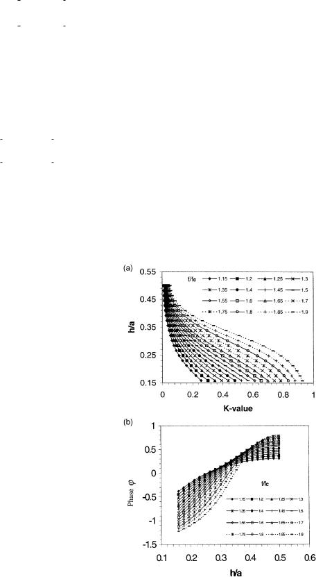
Figure 5 shows the computed K inverter and phase w. values, as functions of the normalized distance from one of the side walls of the waveguide with normalized frequency as a parameter,