

диафрагмированные волноводные фильтры / 1596d94e-3bfd-4f7e-aa88-974c78cc1c0f
.pdfwhereas the surface roughness parameter Ra was reduced to approximately 5 µm, thanks to shot-peen- ing of the internal channels (i.e., abrasive glass/zirconia microspheres of 0.1-mm diameter were pumped through the waveguide channels). The AM-oriented design based on the rotation/tilting of the internal discontinuities was also applied in [17] to develop an 11th-order filter aimed at very-high-throughput satellites or constellations of small satellites. In this case, dimples were inserted at the center of the cavities to improve rejection and spurious-wide range.
Although the dimensional accuracy and resolution of the SLM process make this process more suitable for manufacturing RF filters working below 20–30 GHz, Zhang et al. [24] presented two high-order Chebyshev filters working in the passbands [71, 76] GHz and [81, 86] GHz. The filters were based on the in-line arrangement of 15 and 11 cavities in a WR12 rectangular waveguide coupled by H-plane irises. The two prototypes were manufactured in a copper-tin alloy (CuSn15) powder with a dimensional accuracy of 2%–3% and a surface roughness parameter Ra of approximately 6 µm. These manufacturing properties resulted in a degradation of the frequency responses, above all in terms of passband frequency shift and insertion loss (on the order of 2–3 dB).
A possible way to extend the applicability of the SLM process to the manufacturing of filters working at high frequency bands is to adopt micro-SLM systems. These systems are similar to standard SLM systems, but they make use of powders with smaller particle sizes. This translates into smaller beamspot diameter, laser power, and layer thickness, thus increasing the accuracy, resolution, and surface finishing. A comparison of typical values for some of
the main parameters of the SLM and micro-SLM processes is reported in Table 2.
Salek et al. [25] applied the micro-SLM process to the manufacturing of two W-band fifth-order passband filters based on the in-line arrangement of WR10 waveguide cavities coupled via H-plane irises. The two prototypes were built in stainless steel, with one coated in copper. Figure 13(a) and (b) shows the prototype as built, still attached to the building platform, and after copper plating, respectively. Thanks to the higher accuracy and surface finishing provided by the microSLM process, the measured scattering coefficients compared well with the predicted data, as reported in Figure 13(c) and (d). Remarkably, the filter exhibited an in-band insertion loss of approximately 1 dB, corresponding to an equivalent surface electrical resistivity of 6.7 µΩ cm. This rather low resistivity value was achieved thanks to a measured surface roughness of approximately 2 µm.
Another promising technology for manufacturing high-frequency filters is the 3D screen-printing process presented in [61], the application of which for RF components is currently under evaluation.
The state of the art reported in this section and summarized in Table 3 shows that SLM can represent a viable solution for the monolithic manufacturing of waveguide filters working at high frequency bands, although some technological aspects have to be carefully considered, such as thermal stresses arising during the manufacturing and the staircase effect induced by the layer thickness. Additionally, the SLM process provides the unique capability of free-form fabrication of direct metal parts that can be exploited to miniaturize waveguide subsystems that include several RF functionalities, among which are filters.
(a) |
(b) |
(c) |
|
|
|
Figure 15. An example of filters fabricated with FDM technology [27]. (a) A corrugated low-pass filter. (b) A high-pass filter.
(c) A bandpass filter.
34 |
June 2020 |
Authorized licensed use limited to: Auckland University of Technology. Downloaded on May 28,2020 at 09:46:09 UTC from IEEE Xplore. Restrictions apply.
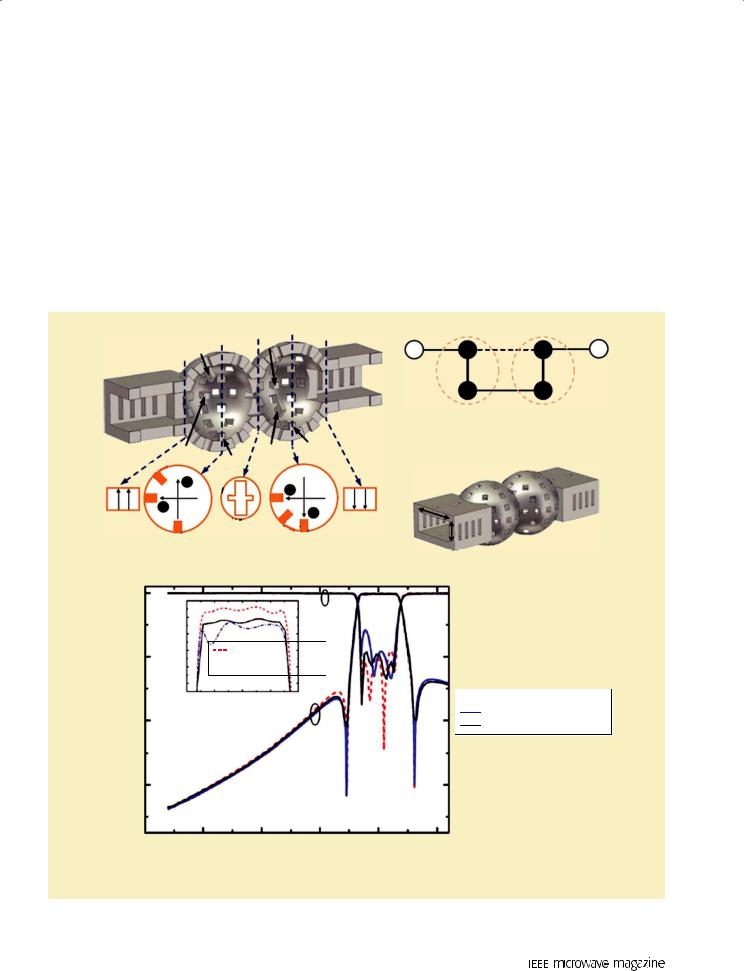
An example of the integration of three distinct RF functionalities in a single miniaturized part is reported in [26]. This paper considers a waveguide subassembly commonly implemented in antenna-feed systems, consisting of the cascade of a 90° H-plane bend, a Ku-/K-band lowpass filter, and a 90° twist. Thanks to the free-form capability of the SLM process, the ninthorder filter, which is based on the topology presented in [21], is mapped into an H-plane bend with constant radius. Then, the geometry is uniformly twisted, yielding to the CAD model shown in Figure 14(a). Three prototypes with different bend radii were manufactured via SLM in aluminum. Figure 14(b) compares the measured and predicted scattering coefficients of the shorter prototype. Along with very good RF performance (i.e., return loss higher than 22 dB, out-of-band rejection higher than 60 dB, and insertion loss lower than 0.15 dB), this component merges the bending and twisting functionalities in the filter structure without any additional mass, volume, or interface demands. This aspect is of the utmost importance in several application domains, including satellite communication and automotive radar.
Development of Plastic Microwave Filters
As discussed previously, several plastic deposition techniques can be used to fabricate microwave components and, in particular, microwave filters. They are the material extrusion process, commonly known as fused
100% Infill
|
Cavity 2 |
|
||
1 |
Cavity 1 |
Cavity 3 |
2 |
|
Port |
Port |
|||
|
|
|||
|
|
(a) |
|
|
100% Infill |
Cavity 2 |
40% Infill |
||
1 |
Cavity 1 |
Cavity 3 |
2 |
|
Port |
Port |
|||
|
|
|||
(b)
Figure 16. An SIW filter with 3D printed dielectric layer [31]. The infill percentage inside the cavities is different in order to change the dielectric constant and losses. (a) 100% infill and (b) 40% infill.
June 2020
deposition modeling (FDM), photopolymerization of a liquid resin, and material jetting, also known as PolyJet.
All these techniques have been investigated in recent years, exposing their strengths and weaknesses. The articles in the literature can be divided into two classes. The first class focuses on the feasibility of standard components built using 3D printing. This study is important to verify the possibility of fast and low-cost prototyping of components by AM. In this group, there are also papers that propose methods to metallize the devices. The second class focuses on new filter configurations that take full advantage of AM flexibility. These components can be easily built by 3D printing, but they are difficult to fabricate with traditional subtractive techniques.
Studies on Plastic AM Technologies for Filters
Historically, the first attempts to use plastic 3D printing study the feasibility of different technologies to fabricate microwave components and then analyze the results. The available literature can be classified according to technology. For FDM technology, one of the first attempts was presented in [27]. The authors fabricated a corrugated low-pass filter, a high-pass
(a)
|
0 |
|
|
|
|
|
|
|
|
Simulated |
|||
|
–10 |
|
|
|||
|
|
|
Measured |
|||
LossInsertion(dB) |
–20 |
|
|
|||
|
|
|||||
|
|
|
|
|||
|
|
|
(dB)LossReturn |
|||
–30 |
0 |
|||||
|
|
|||||
|
–40 |
|
|
–10 |
|
|
|
–50 |
|
|
–20 |
|
|
|
–60 |
|
|
–30 |
|
|
|
–70 |
|
|
–40 |
|
|
|
–80 |
|
|
–50 |
|
|
|
–90 |
|
|
–60 |
|
|
18.218.7 19.2 19.7 20.2 20.7
Frequency (GHz)
(b)
Figure 17. A four-cavity waveguide filter fabricated with SLA technology [36]. (a) The filter with an internal view.
(b) The measurements and simulations.
35
Authorized licensed use limited to: Auckland University of Technology. Downloaded on May 28,2020 at 09:46:09 UTC from IEEE Xplore. Restrictions apply.
filter, and an inductive iris bandpass filter. Figure 15 shows the internal parts (air) and the external parts of the filters. To metallize the internal surfaces, all devices were split into two halves, and the flanges were fabricated separately and then attached to the main bodies. In [28], the authors assessed the technology by building two bandpass filters, a four-pole inductive iris filter and a two-pole with inductive posts (i.e., an E-plane filter), and a helical resonator was used to test the dielectric constant of materials. In both articles, there is a slight frequency shift and return loss deterioration in the experimental responses compared with simulated ones. This result means that the dimensional accuracy is not enough to avoid tuning elements, especially for narrow band filters. However, these articles show that polymer-based AM machines, such as cheap FDM printers, can be successfully used in university laboratories for rapid prototyping of RF components aimed at educational activities and for low-cost manufacturing of measurement equipment (such as waveguide jigs used in network analyzers setups). In [29], other cavity filtering devices, working in the Ka band and made through
FDM, were presented. The results, in terms of accuracy and frequency shift, are comparable with other works. In [30], a 3D printer was used to manufacture the waveguide enclosure of a high permittivity dielectric resonator. In this case, the frequency accuracy and losses of the measured single pole filter mostly depended on the dielectric resonator.
In [31], [32], and [33], the possibility of using the infill percentage for local control of the dielectric constant and loss tangent of the printed material was demonstrated through the AM of a substrate integrated waveguide (SIW) (Figure 16). To this end, two different substrates with different infill percentages (40% and 100%) were printed and used to build two SIW filters with the same filtering response.
FDM printers are less expensive than SLA or PolyJet printers. The filament is also very cheap, and PLA is eco-friendly. However, because the nozzle diameter is usually 0.25–0.4 mm and the layer thickness is in the range of 0.1–0.25 mm, mechanical accuracy is not very high. The surface roughness is also quite high, meaning that this technology is not very attractive for the fabrication of microwave components.
y
x
z
a |
a |
|
(a)
S-Parameters (dB)
|
|
|
|
|
(b) |
|
|
|
|
|
(c) |
|
0 |
|
|
|
|
|
|
|
|
|
|
|
|
–10 |
|
|
|
|
|
|
|
|
|
|
|
|
–20 |
|
|
|
|
|
|
|
|
|
|
|
|
–30 |
|
|
|
|
|
|
|
|
|
|
|
|
–40 |
|
|
|
|
|
|
|
|
|
|
|
|
–50 |
|
|
|
|
|
S11 (Measured) |
|
|
S21 (Measured) |
|
||
|
|
|
|
|
|
|
|
|||||
|
|
|
|
|
S11 (Simulated_Original Filter Model) |
|
||||||
|
|
|
|
|
|
|
||||||
–60 |
|
|
|
|
|
S21 |
(Simulated_Original Filter Model) |
|
||||
|
|
|
|
|
|
|||||||
|
|
|
|
|
|
S11 |
(Simulated_Modified Filter Model) |
|
||||
–70 |
|
|
|
|
|
S21 |
(Simulated_Modified Filter Model) |
|
||||
|
|
|
|
|
|
|||||||
75 |
80 |
85 |
90 |
95 |
100 |
105 |
110 |
|
||||
Frequency (GHz)
(d)
Figure 18. The w-band waveguide filter [39]. The (a) external and (b) cut views. (c) The filter. (d) The measurements and simulations.
36 |
June 2020 |
Authorized licensed use limited to: Auckland University of Technology. Downloaded on May 28,2020 at 09:46:09 UTC from IEEE Xplore. Restrictions apply.
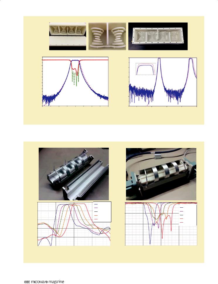
Another interesting technology is photopolymerization and, in particular, SLA. In earlier works, [3], [34], [35], tests of simple waveguide cavities and filters were completed. The first example is a single cavity working in the Ku band, where the authors split the cavity without perturbing its current flow. Other tests concern horizontally and vertically shaped multicavity filters. The most complex device is the four-port waveguide filter shown in Figure 17. The authors obtained quite good results, with a frequency shift for the response of approximately 0.15% and Q for all prototypes in the range of 3,000–3,500. The experimental return loss is lower than the simulated one, but this difference is comparable with other fabrication processes. In [33] and [38], a single cavity and a three-pole waveguide filter working in the X band were presented. The cavities were shaped to make the metallization process easier. In this case, the frequency shift is around 0.15%, and the measured Q is 3,700.
Other tests have been carried out at higher frequencies. For example, in [38], a six-cavity filter with inductive irises working in the W band was presented. The experimental response is shifted at higher frequencies. The
authorsstatethatthe problem is |
|
|
|
a metallization thicker than |
|
|
|
predicted, which reduced the |
|
|
|
length of the cavities. Another |
|
|
|
example of a fifth-order wave- |
|
|
|
guide filter operating in the |
|
|
|
W band is shown in [39]. The fil- |
|
|
|
ter was fabricated as a single |
|
|
|
piece with many apertures for |
|
|
|
the metallization of internal |
|
|
|
surfaces (Figure 18). Consider- |
|
|
|
ing that the prototype does not |
|
|
|
use any tuning elements, the |
|
|
|
experimental results show very |
|
0 |
|
good agreement in terms of the |
|
–10 |
|
simulations, with only a small |
|
||
|
|
||
shift toward lower frequencies |
(dB) |
–20 |
|
of the passband. |
–30 |
||
The results obtained with SLA |
-Parameters |
||
|
|||
are very good, thanks to the |
–40 |
||
higher accuracy of this technol- |
–50 |
||
ogy in comparison with FDM. In |
|||
|
|||
S |
–60 |
||
fact, the usual laser spot diameter |
|||
|
|||
is 50–100 µm, and the layer thick- |
|
–70 |
|
ness is 25–200 µm, depending on |
|
|
the printer. The roughness is also |
–80 |
|
33 |
||
lower with respect to FDM, as it |
||
|
||
is on the order of a few microns. |
|
|
Considering its good tradeoff |
|
|
between cost and mechanical |
|
|
accuracy, this technology is one |
|
|
June 2020 |
|
of the most used and most promising for the fabrication of 3D printed components.
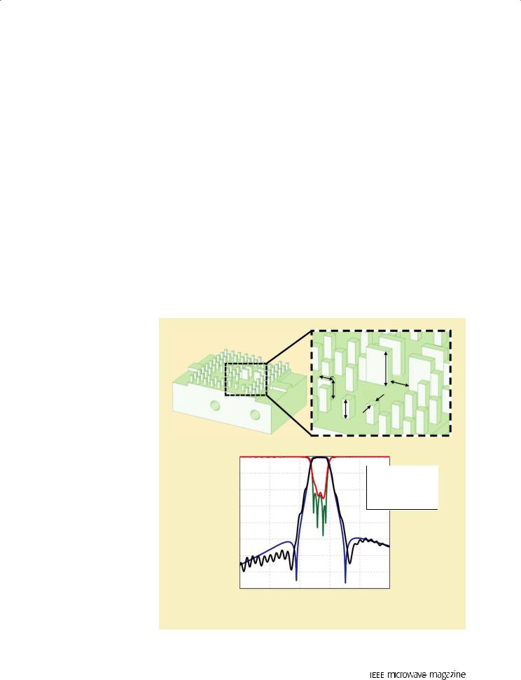
Some attempts have also been made using PolyJet technology. For example, in [40], basic single and multicavity waveguide filters were fabricated. PolyJet’s accuracy is higher than that of either FDM or SLA. In particular, both the lateral and vertical resolutions are approximately 15 µm, with surface roughnesses that vary from 0.5 µm for horizontal surfaces to 3 µm for vertical ones. The latter figure is mainly due to the layer- by-layer deposition. PolyJet technology has also been used to build planar filters, by printing the substrate, as in [41]. However, the high loss tangent of the resin gives quite lossy devices. A very recent work shows an application of PolyJet printing in the Ka band. [42] In this case, a gap waveguide (i.e., with noncontinuous side walls), four-pole filter was fabricated and tested (Figure 19). As can be seen, there is capacitive crosscoupling between cavities 1 and 4 that creates the two transmission zeros. This experiment shows that the 3D printing of such devices is feasible, and the experimental results are in good agreement with the theoretical results. The accuracy of PolyJet technology is higher than FDM and SLA. In fact, the typical lateral resolution
Pij_l |
|
iris_h |
|
|
iris_w |
|
Pij_h |
H_l |
|
|
|
|
H_h |
|
 S11 Simulated
 S11 Measured
 S21 Simulated
 S21 Measured
37 38
37
Authorized licensed use limited to: Auckland University of Technology. Downloaded on May 28,2020 at 09:46:09 UTC from IEEE Xplore. Restrictions apply.
and layer thickness are in the range of 15–30 µm. The measured roughness is approximately 0.5 µm.
In [43], an aerosol jet printing process was used to build a planar filter. This technique is relatively recent and consists of the jetting of a polyamide resin, which requires only the postprocessing step of high-temper- ature curing. This step is also called imidization. The advantage of this technique is that the same printer can be used to fabricate both the dielectric and conductive layers.
Because all the devices described previously are made of plastic, they must be metallized to realize conductive walls. Some proposed techniques are summarized in the following.
•Silver painting [27]–[29]. The device is metallized by painting with a silver ink. It is possible to apply more than one layer after the previous layers have dried. Silver painting is the simplest metallization, and the final conductivity of the surfaces
In 1 |
5 Out |
2 3 4
Figure 20. A five-cavity filter that uses single-mode spherical resonators [45].
38
is rather low, in the range of 105–106 S/m; thus, the losses are higher than those of standard metal components.
•Silver painting + electrolytic copper [3], [34], [37]. This method, fully described in [44], applies a doublestep process to metallized components. The first step is silver painting of the surfaces. This layer acts as an activation layer for the subsequent electrolytic copper plating, because electrolytic processes can be done only on conductive surfaces. The thickness of the copper layer can be up to several tenths of microns, depending on the duration of the deposition, and the dimensions of the device must be adjusted to compensate for the thickness of this layer. With this method, a conductivity very close to that of pure copper and a roughness below 1 µm can be obtained. As a consequence, the measured losses are usually comparable with the losses of traditional metal components. This process is also easy to implement and very low cost. As reported in [44], the metallization has a good adhesion to the plastic, and the device is resistant against peeling.
•Electroless copper deposition. This is a more complicated and expensive process, because it needs some activation before copper deposition. This process has been used with success to metallize components on internal surfaces, without the need to divide them into two or more parts, as shown in the work presented in the next section.
The copper can also be plated with a 100-nm-thick gold layer (as in [39]) to protect the device from oxidation.
Innovative Filter Design Using Additive Manufacturing on Plastic and Ceramics
Building on early studies that showed the feasibility of 3D-printed microwave devices, innovative microwave filter designs have been proposed that take advantage of the flexibility of AM technologies.
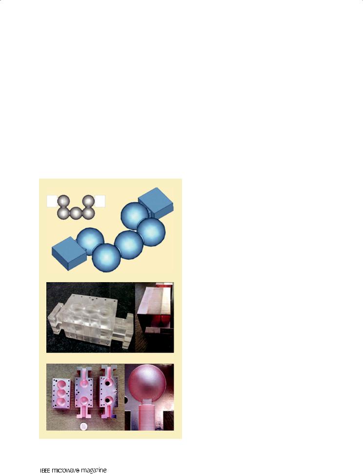
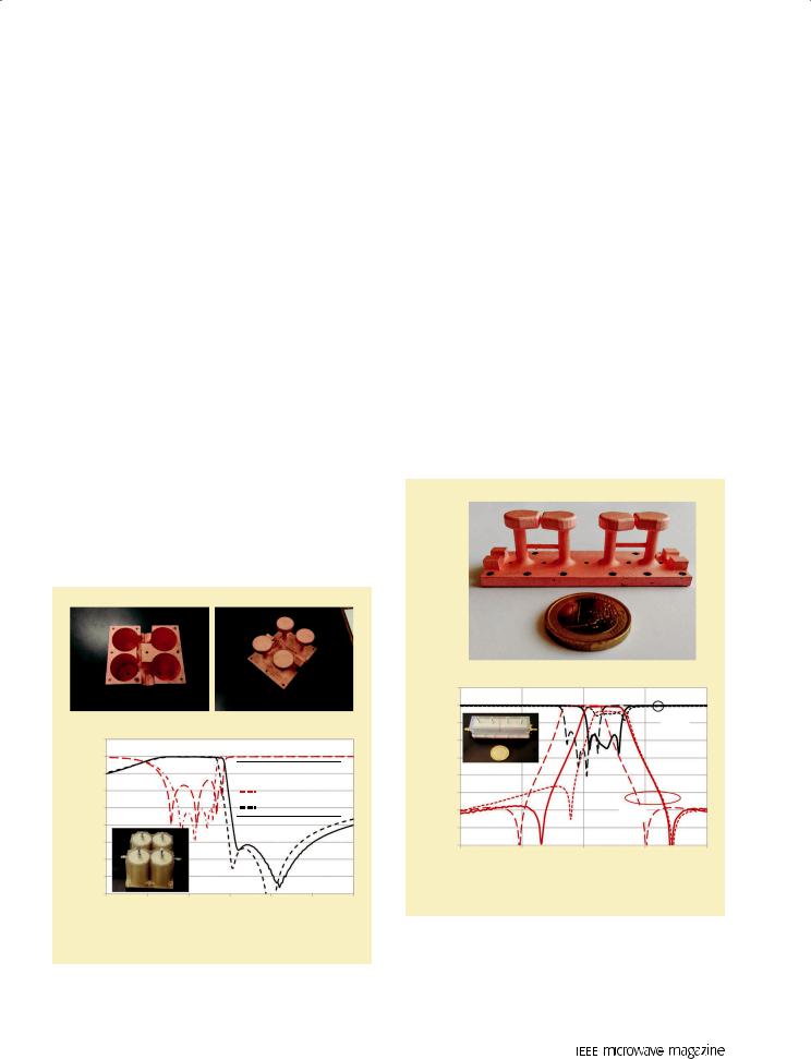
The first example concerns spherical resonator filters [45]–[47]. These can be easily built using AM, yet they are relatively complex to build with traditional subtractive manufacturing. In [45], a single-mode cavity filter operating in the X band was designed (Figure 20). It uses a fundamental TM101 mode that exhibits a high Q. In [46], [47], a dual-mode cavity filter is proposed (Figure 21). In this case, the filter is fabricated as a single piece with apertures on the external walls to facilitate metallization of the internal surfaces by electrolytic copper deposition. The apertures are strategically placed where the currents are not perturbed. The experimental results are quite good, with a slightly higher insertion loss in the passband (0.3 dB measured versus 0.1 dB simulated). The filter was tuned using small wires inserted inside the apertures in the lateral
June 2020
Authorized licensed use limited to: Auckland University of Technology. Downloaded on May 28,2020 at 09:46:09 UTC from IEEE Xplore. Restrictions apply.
walls of the device. In [49], a four-pole spherical cavity bandpass filter, similar to that proposed in [45], was built as a single piece and then metallized using an electroless nickel/copper plating. The experimental losses were higher with respect to the simulations.
A thorough discussion of hemispherical resonators is presented in [49]. The authors analyze many aspects of this approach, proposing different cavity arrangements to improve the out-of-band attenuation. Moreover, they analyze the coupling apertures among resonators. The prototypes were fabricated as single blocks and metallized using electroless copper deposition and silver plating. Experimental results are very good in comparison with the simulations.
Helical resonator filters are another type of filter that can take advantage of AM [50]. Helical resonators are useful at very low frequencies (usually VHF and UHF bands) and, traditionally, are made by winding a wire by hand. 3D printing can automate the production while improving accuracy. In [50], the authors propose a halfwavelength helix with variable width (Figure 22). The shape of the helix is used to increase the filter bandwidth.
In [51], an innovative tunable E-plane filter, fabricated using FDM technology and operating at around 5.7 GHz, is proposed (Figure 23). In this structure, the filter is composed of a waveguide, divided into two halves, along with a sort of spiral ribbon that can rotate. Part of the spiral ribbon is inside the
E
(Ms1)
|
0 |
(dB) |
–20 |
|
|
Parameters-S |
–40 |
|
|
|
–60 |
C1
(M12) T2 |
|
|
|
T1 |
C2 |
|
T4 |
|||
|
|
|
|
|
|
|
||||
C1 |
|
1 |
|
(M14) |
|
3 |
E |
|||
T2 |
|
|
|
T3 |
||||||
|
E |
|
|
|
|
|
|
E |
||
2 |
|
|
|
|
|
C2 |
4 |
|
||
|
|
|
|
|
|
|
|
|
||
|
|
T1 |
|
|
|
(M23) |
(M34) T4 |
|||
Resonator 1 |
Iris |
Resonator 2 |
||||||||
|
|
|
|
|
|
(a) |
|
|
|
|
|
|
0 |
|
|
|
|
|
|
|
|
|
–0.2 |
|
|
|
|
|
|
S11 |
||
(dB) |
–0.4 |
|
|
|
|
|
|
|
|
|
–0.6 |
|
|
|
|
|
|
|
|
||
|
|
|
Simulated |
|
|
|
||||
21 |
|
|
|
|
|
|
||||
|
|
|
|
|
Measured Without Tuning |
|
||||
S |
–0.8 |
|
|
|
|
|||||
|
|
|
Measured With Tuning |
|
||||||
|
|
–1 |
|
|
|
|
||||
|
|
|
|
|
|
|
|
|
|
|
|
|
|
|
|
|
|
|
|
|
|
|
|
9.8 |
9.9 |
10 |
10.1 |
10.2 |
|
|
||
|
|
|
Frequency (GHz) |
|
|
|
||||
|
|
|
|
|
|
|
|
|
S21 |
|
8 8.5 9 9.5
Frequency (GHz)
(d)
S |
Ms1 |
M14 |
M4L |
L |
|
1 |
4 |
||
|
|
M12 |
M34 |
|
|
|
2 |
3 |
|
|
|
M23 |
|
|
|
Resonator 1 |
Resonator 2 |
|
|
|
|
(b) |
|
|
a
(M4L)
b
(c)
 Simulated
Measured Without Tuning
Measured With Tuning
10 10.5
Figure 21. A dual-mode spherical cavity filter [46] and [47]. (a) The inside view. (b) The coupling scheme. (c) A 3D view.
(d) The measurements and simulations.
June 2020 |
39 |
Authorized licensed use limited to: Auckland University of Technology. Downloaded on May 28,2020 at 09:46:09 UTC from IEEE Xplore. Restrictions apply.
|
|
|
(a) |
|
(b) |
|
|
0 |
|
|
|
|
0 |
|
|
|
|
|
|
|
|
–10 |
|
|
|
|
–20 |
(dB) |
|
|
|
|
|
|
–20 |
|
|
|
|
|
|
|
|
|
|
|
|
|
Parameters |
–30 |
|
|
|
|
–40 |
|
|
|
|
S |
|
|
|
–40 |
|
|
|
(dB) |
|
|
|
|
|
21 |
|
|
|
|
|
|
|
–60 |
|
|
–50 |
|
|
|
|
|
|
|
|
|
|
|
|
S- |
–60 |
|
|
|
|
–80 |
|
–70 |
|
|
|
|
|
|
|
|
|
|
|
|
|
–80 |
|
|
|
|
–100 |
|
0.4 |
0.45 |
0.5 |
0.55 |
0.6 |
|
Frequency (GHz)
(d)
Figure 22. A helical resonator filter, working in the UHF band [50].
(c)
|
0 |
|
|
(dB) |
–1 |
|
|
–2 |
|
|
|
S |
–3 |
|
|
21 |
|
|
|
|
–4 |
|
|
|
–5 0.49 |
0.5 |
0.51 |
Frequency (GHz)
0.2 |
0.4 |
0.6 |
0.8 |
1 |
Frequency (GHz)
(e)
(dB)
Waveguide
Filter Upper
Part
Spiral Ribbon
0
–10
–20
–30
Waveguide
Filter Lower Part
S21 pos5
S21 pos4
S21 pos3
S21 pos2
S21 pos1
(dB)
0
–10
–20
S21 pos5
S21 pos4
S21 pos3
S21 pos2 S21 pos1
–40 |
|
|
|
|
–30 |
|
|
|
|
|
|
|
|
|
|
|
|
|
|
–50 |
5.25 |
5.75 |
6.25 |
6.75 |
–40 |
5.25 |
5.75 |
6.25 |
6.75 |
4.75 |
4.75 |
||||||||
|
|
(GHz) |
|
|
|
|
(GHz) |
|
|
|
|
(a) |
|
|
|
|
(b) |
|
|
Figure 23. A tunable E-plane filter with a rotating spiral ribbon to change the band [51]. The experimental results are for different positions of the spiral ribbon. (a) The transmission coefficient. (b) The reflection coefficient.
40 |
June 2020 |
Authorized licensed use limited to: Auckland University of Technology. Downloaded on May 28,2020 at 09:46:09 UTC from IEEE Xplore. Restrictions apply.
waveguide, and, with its rotation, the band of the filter can be shifted. The experimental results show the validity of the principle.
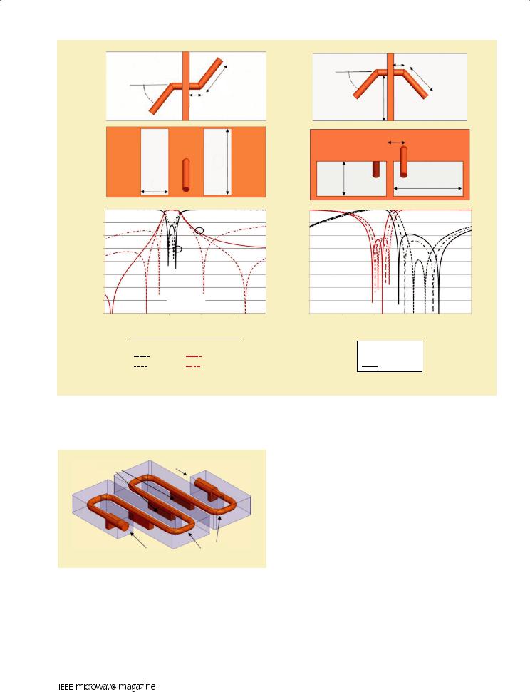
Another filter geometry that can take full advantage of AM is the combline layout. Usually, a combline filter is made of several parts, such as a housing, a cover, and a number of internal posts, one for each cavity, that are attached inside the housing. With AM, only two parts are needed, a main body that contains the resonators and a cover. The resonators can also be loaded with capacitive discs, thus resulting in the so-called mushroom shape, to reduce the length of the posts and improve the out-of-band attenuation. In [52] and [54], a basic doublet, capable of responses with two poles and two transmission zeros, is presented. The coupling between the two resonators is achieved by a conductive rod attached to the mushroom stems. In [54], the basic structure was extended by cascading two basic doublets (Figure 24), demonstrating the possibility of building higher-order filters. As can be seen, with this structure it is simple to place two transmission zeros above the passband of the filter.
Another approach using mushroom-shaped resonators is presented in [55]. In this case, inductive and capacitive coupling between two resonators is achieved by a rod connecting the stems and by reducing the distance between the two “caps,” respectively (Figure 25). The resulting coupling generates a transmission zero. This zero can be placed above or below the band of the
|
|
(a) |
|
|
|
|
(b) |
|
|
|
(dB) |
10 |
|
|
|
|
|
|
|
|
|
0 |
|
|
|
|
|
|
|
|
|
|
|
|
|
|
|
|
|
|
|
|
|
Parameters |
–10 |
|
|
|
|
|
S11 |
|
S21 |
|
|
|
|
|
|
|
|
||||
–40 |
|
|
|
|
|
S11 Simulation |
|
|||
|
–20 |
|
|
|
|
|
|
|||
|
–30 |
|
|
|
|
|
S21 Simulation |
|
||
Scattering |
–50 |
|
|
|
|
|
|
|
|
|
–60 |
|
|
|
|
|
|
|
|
|
|
|
|
|
|
|
|
|
|
|
|
|
|
–70 |
|
|
|
|
|
|
|
|
|
|
–800.7 |
0.75 |
0.8 |
0.85 |
0.9 |
|
0.95 |
1 |
||
|
|
|
Frequency (GHz) |
|
|
|||||
(c)
Figure 24. A four-pole “mushroom” filter working in the UHF band [54]. (a) The main body. (b) The cover. (c) A comparison between measurements and simulations.
June 2020
Building on early studies that showed the feasibility of 3D-printed microwave devices, innovative microwave filter designs have been proposed that take advantage of the flexibility of AM technologies.
filter depending on the magnitude of the electric and magnetic couplings. The scattering parameters illustrated in Figure 25(b) show that the structure is able to generate the two transmission zeros. There is a small shift of the band of the filter toward higher frequencies.
In [56] and [57] a very compact filtering structure is presented. The filter consists of a single septum, with one or more apertures, and two small resonant posts (Figure 26). A very precise positioning of the transmission zeros is possible in this filter by properly selecting the shape and dimension of the apertures and posts. This structure can be used to add
|
|
|
(a) |
|
|
(dB) |
10 |
|
|
|
|
0 |
|
|
|
|
|
|
|
|
|
|
|
Parameters |
–10 |
|
|
|
S11 |
–40 |
|
|
|
|
|
|
–20 |
|
|
|
|
|
–30 |
|
|
|
|
Scattering |
–50 |
|
|
|
|
–60 |
|
|
S21 |
|
|
|
|
|
|
||
|
–70 |
|
|
|
|
|
–801.6 |
1.7 |
1.8 |
1.9 |
2 |
|
|
|
Frequency (GHz) |
|
|
(b)
Figure 25. A four-pole “mushroom” filter with mixed electric and magnetic couplings working at 1.8 GHz [55].
(a) The main body of the filter. (b) A comparison among simulations (dashed curves), measurements without tuning (dotted curves), and measurements with tuning (continuous).
41
Authorized licensed use limited to: Auckland University of Technology. Downloaded on May 28,2020 at 09:46:09 UTC from IEEE Xplore. Restrictions apply.
L0
LP
|
LP |
|
|
L0 |
H |
|
S
h
w |
h |
w |
|
|
(dB) |
10 |
|
|
|
|
|
S21 |
|
|
0 |
|
|
|
|
|
|
|
||
|
|
|
|
|
|
|
|
|
|
Parameters |
–10 |
|
|
|
|
|
|
|
|
–40 |
|
|
|
|
|
|
|
|
|
|
–20 |
|
|
|
|
|
|
|
|
|
–30 |
|
|
S11 |
|
|
|||
Scattering |
–50 |
|
|
h = 9.5 mm |
|
|
|||
–70 |
|
|
|
|
|||||
|
–60 |
|
|
= 43° |
|
|
|
|
|
|
|
|
|
|
|
|
|
||
|
–80 7 |
8 |
9 |
|
10 |
11 |
12 |
||
|
|
|
|
Frequency (GHz) |
|
|
|||
|
|
|
|
|
|
|
|
|
|
|
|
|
|
w = 2 mm |
|
|
w = 2 mm |
|
|
|
|
|
|
|
|
|
|||
|
|
|
|
w = 4 mm |
|
w = 4 mm |
|
||
|
|
|
|
w = 8 mm |
|
w = 8 mm |
|
||
|
|
|
|
|
|
|
|
|
|
(a)
Scattering Parameters (dB)
10 |
|
|
|
|
|
0 |
|
|
|
|
|
–10 |
|
|
|
|
|
–20 |
|
|
|
|
|
–30 |
|
|
|
|
|
–40 |
|
|
|
|
|
–50 |
|
|
|
|
|
–60 |
|
|
|
|
|
–70 |
|
|
|
|
|
–80 7 |
8 |
9 |
10 |
11 |
12 |
|
|
Frequency (GHz) |
|
|
|
 S = 1.2 mm
 S = 1.6 mm
S = 2 mm
(b)
Figure 26. A very compact filtering structure composed of a single iris and two posts. The shape and size of the apertures and posts give the behavior of the filter [56]. (a) One transmission zero above and one below the passband of the filter (b) Two transmission zeros in the upper stop band.
Supports Port
Port |
Coaxial |
|
Lines |
||
|
Figure 27. An inline coaxial filter where supports for the coaxial line behave as coupling elements [58].
a mild filtering behavior in existing microwave systems. Indeed, if the filter is inserted between the junction of two waveguides of an existing system, the system dimension increases only by the septum thickness (0.5 mm).
A filtering structure with high shaping flexibility is presented in [58]. In this case, a coaxial line is attached to the main body with supports. The portions of the lines in the free air act as resonators, whereas the supports are the coupling elements (Figure 27). The desired filter response is obtained by adjusting the length of the resonators and the length of the supports. Note that this structure offers a high degree of design flexibility in terms of shape. Indeed, the structure can be designed straight or bent as in Figure 27 to obtain a more compact structure. Like the other filters presented in this section, this structure can be easily made with AM, whereas it is relatively complex to build with traditional subtractive technologies. The main characteristics of some of the filters in plastic AM presented in this paper are summarized in Table 4.
Exploitation of the free-form capability of AM has also been investigated in view of the miniaturization
42 |
June 2020 |
Authorized licensed use limited to: Auckland University of Technology. Downloaded on May 28,2020 at 09:46:09 UTC from IEEE Xplore. Restrictions apply.

TABLE 4. A comparison of filters developed through plastic AM.
|
|
|
Center |
Fractional |
|
|
|
Frequency |
Bandwidth |
Reference |
Filter Order/Geometry |
3D Technology |
(GHz) |
(%) |
|
|
|
|
|
[27] |
Fourth-order filter/rectangular waveguide inductive iris filter |
FDM silver painted |
13,85 |
2.88 |
[36] |
Fourth-order filter/stacked rectangular cavities |
SLA electroplated |
19.68 |
1.14 |
[39] |
Fifth-order filter/rectangular waveguide cavities |
SLA copper plated |
87.5 |
11.5 |
[42] |
Fourth-order filter/groove gap waveguide |
PolyJet electroplated |
35.65 |
1.4 |
[50] |
Fourth-order filter/helical resonators |
SLA copper/silver plated |
0.5 |
4 |
[51] |
Fourth-order filter/reconfigured central frequency |
FDM silver painted |
5.64 |
6.4 |
[54] |
Fourth-order filter/mushroom-shaped resonators |
SLA copper plated |
0.81 |
6 |
[58]. |
Fourth-order filter/coaxial filter |
SLA copper plated |
3 |
1.6 |
of low-frequency filters by applying vat photopolymerization techniques, such as SLA and DLP, to ceramic materials. In [59], DLP was used to build an X-band, two-pole dielectric resonator filter in a single alumina part, which was subsequently externally metal-plated. The main advantage of this solution is not having dielectric rods mounted within metal cavities, thus leading to a more robust device, especially with respect to temperature variations. The possibility of manufacturing ceramic parts with complex shapes was also exploited in [60] to develop a tunable filter working in the Ku band. The frequency tunability of the filter is based on the synchronous rotation of zirconia perturbers inserted in the waveguide resonators. The optimization of the filter performance in terms of constant bandwidth over a wide tuning range was achieved by manufacturing the zirconia inserts with complex shapes through SLA.
Conclusions
This article showed that AM technologies are beginning to be successfully applied in the development of high-performance filters with novel topologies working from a few gigahertz to approximately 20–30 GHz (K and Ka bands). Examples are filters with shaped-waveguide resonators directly built in aluminum through SLM [9] and stacked-cavity filters printed by SLA. [36] The unique free-form feature of AM processes has been exploited for the successful implementation of filter layouts that are at the edge of the capacity of conventional machining, such as mushroom cavity filters coupled via suspended wires [54], and the integration of multiple RF functionalities in monolithic filtering structures [26]. In recent years, exploitation of the most accurate AM processes, such as SLA [39] and micro-SLM [25], have made possible the application of AM technologies at higher frequencies, such as the W band.
Research on AM for RF components is currently focused on the following main areas: 1) the optimization of AM processes for RF applications (e.g., surface roughness, metallization, and selection of proper materials); 2) redesign of canonical RF architectures according to guidelines for AM-ori- ented design (e.g., smooth surfaces, suited geometries); and 3) the development of new classes of components that exploit the high flexibility of AM in manufacturing new geometries that are difficult or impossible to manufacture via conventional subtracting techniques. Most current research focuses on just one of these aspects. It is our opinion that the development of filters with increased performance will benefit from research activities focused on all of the aforementioned aspects and based on a concurrent engineering approach that encompasses multiple competencies, among them RF engineering, material science, and mechanical and production engineering. As an example, SLM has already been proven to be suitable for manufacturing all-metal filters with adequate electrical surface resistivity (e.g., 10–20 µΩ cm for AlSi10Mg alloy without additional coating), surface roughness as low as 5 µm after shot-peening of the internal faces, and dimensional accuracy on the order of 30–60 µm.
However, it must be noted that all these properties depend strongly on the process and postprocess parameters as well as the filter geometry. For example, the staircase effect arising from the discretization of the filter profile along the building direction affects both the surface roughness and the dimensional accuracy. As a rule of thumb, the faces of the internal channels should be inclined at least 45°. Indeed, if filter architectures are redesigned according to this recommendation, no supporting structures for the internal surfaces are needed and the risk of warping and cracks is minimized.
June 2020 |
43 |
Authorized licensed use limited to: Auckland University of Technology. Downloaded on May 28,2020 at 09:46:09 UTC from IEEE Xplore. Restrictions apply.