

диафрагмированные волноводные фильтры / b0b57036-0482-48fc-8baa-0683bd585b25
.pdf878 |
IEEE TRANSACTIONS ON MICROWAVE THEORY AND TECHNIQUES, VOL. 67, NO. 3, MARCH 2019 |
||||||||||||||||
|
|
|
|
|
|
|
|
|
|
|
|
|
|
|
|
|
|
|
|
|
|
|
|
|
|
|
|
|
|
|
|
|
|
|
|
|
|
|
|
|
|
|
|
|
|
|
|
|
|
|
|
|
|
|
|
|
|
|
|
|
|
|
|
|
|
|
|
|
|
|
|
|
|
|
|
|
|
|
|
|
|
|
|
|
|
|
|
|
|
|
|
|
|
|
|
|
|
|
|
|
|
|
|
|
|
|
|
|
|
|
|
|
|
|
|
|
|
|
|
|
|
|
|
|
|
|
|
|
|
|
|
|
|
|
|
|
|
|
|
|
|
|
|
|
|
|
|
|
|
|
|
|
|
|
|
|
|
|
|
|
|
|
|
|
|
|
|
|
|
|
|
|
|
|
|
|
|
|
|
|
|
|
|
|
|
|
|
|
|
|
|
|
|
|
|
|
|
|
|
|
|
|
|
|
|
|
|
|
|
|
|
|
|
|
|
|
|
|
|
|
|
|
|
|
|
|
|
|
|
|
|
|
|
|
|
|
|
|
|
|
|
|
|
|
|
|
|
|
|
|
|
|
|
|
|
|
|
|
|
|
|
|
|
|
|
|
|
|
|
|
|
|
|
|
|
|
|
|
|
|
|
|
|
|
|
|
|
|
|
|
|
|
|
|
|
|
|
|
|
|
|
|
|
|
|
|
|
|
|
|
|
|
|
|
|
|
|
|
|
|
|
|
|
Fig. 29. Fabricated coupler. (a) Top-view photograph. (b) X-ray photograph of inside of LTCC. The X-ray photograph has been taken from downside to show the coupling apertures.
Fig. 30. Simulation and measurement results of V-LIW coupler.
results of the optimized coupler are illustrated in Fig. 30. As it can be seen from this figure, the designed coupler provides about 20-dB (22 dB measured) coupling from 58 to 62 GHz, and the return loss and isolation in this band are better than 17 dB (13.3 dB measured) and 32.5 dB (25 dB measured), respectively. It should be noted that the level of coupling is proportional to the size/number of the side apertures. In the vertical arrangement, these parameters are limited by the thickness of the LTCC stack. The more layers we use or the higher frequency we go to, the higher the maximum achievable coupling level becomes.
C. V-LIW Filter
The SIW has been widely used in the design of mmwave directed-coupled-cavity filters [43]–[47]. In these filters, the cavity resonators are usually coupled to each other using iris post walls [48] or apertures in case cavities are located in different layers [49].
Fig. 31. Geometry of V-LIW fifth-order W-band filter and sample layers.
In order to show the suitability of the proposed V-LIW in filter realization, we have designed two filters: a simple fifth-order fully V-LIW direct-coupled-resonator filter at W-band and also a ninth-order filter at V-band which has the 90◦ bend and transition to CPW.
1) Fifth-Order W-Band Chebyshev Filter: The geometry of the designed filter based on V-LIW is illustrated in Fig. 31. It is composed of five cavity resonators in a row. These cavities are coupled by iris discontinuities which are formed by printed metals. The design parameters of this filter are the length of cavities (li) and irises’ opening length (di). In order to determine these parameters, a method that is a combination of the methods in [50] and [51] has been used. The design procedure is quite straightforward and it can be summarized in the following steps.
Step 1: Solve the following equation to determine the midband guided wavelength λ0:
λgl sin |
π λg0 |
+ λgh sin |
π λg0 |
= 0 |
(8) |
λgl |
λgh |
where λgl and λgh are the guided wavelength at lower and upper cutoff frequencies, respectively.
Step 2: Find the normalized iris reactances at λg0 by
|
|
√ |
L |
|
|
|||
|
|
|
|
|
|
|
|
|
Xi,i+1 = |
|
gi gi+1 |
|
|
, i = 0 : n |
(9) |
||
1 − |
L2 |
|||||||
|
gi gi+1 |
|
|
|
||||
where n is the order of the filter, gi is Chebyshev’s low-pass ith element [51], and L is defined by
L = |
π |
|
λgl |
− |
λgh |
(10) |
ω |
λgl |
+ |
λgh |
|||
|
|
|
|
|
|
in which ω is the passband edge of the prototype low-pass filter.
Step 3: Determine the length of cavity resonators (lci ) by
lci = |
λg0 |
− |
λg0 |
[tan−1[2Xi+1]+tan−1[2Xi ]]. (11) |
2 |
4π |
ISAPOUR AND KOUKI: V-LIW AND TRANSITIONS FOR mm-WAVE APPLICATIONS
Step 4: Obtain the iris’s opening length (di ). This is accomplished by finding di for which the following equation provides us the same Xi as in Step 2 [52]:
|
a |
|
π d |
|
|
|
|
|
|
|
|
|
|
|
|
|
|
|
|
|
|
|
|
|
|
|
|
|
|||
Xi = |
|
tan2 |
|
|
|
|
|
|
|
|
|
|
|
|
|
|
|
|
|
|
|
|
|
|
|
|
|
|
|
|
|
λg0 |
2a |
|
|
|
|
|
|
|
|
|
|
|
− 1 sin2 |
πa |
|
|
|
|
|
|
|||||||||||
|
× 1 + |
4 |
|
|
|
|
|
|
1 |
2a |
2 |
|
|
|
|
|
|
||||||||||||||
|
|
|
|
3 |
|
|
|
|
|
|
|
|
|
|
|
|
|
|
|
|
|
d |
|
|
|
|
|
|
|||
|
|
|
|
|
|
|
|
|
|
|
|
|
|
2 |
|
|
|
|
|
|
|
|
|
|
|
||||||
|
|
|
|
|
1 − |
|
3λ |
|
|
|
|
|
|
|
|
|
|
|
|
||||||||||||
|
+ |
2 |
|
a |
|
|
1 |
− |
4 |
|
(α) − β |
F(α) |
|
|
|
|
|
|
|||||||||||||
|
|
λ |
|
|
|
π |
E |
α2 |
|
|
|
|
|
|
|
|
|
|
|
|
|
||||||||||
|
|
|
|
|
|
|
|
2 |
|
|
|
|
|
|
|
|
|
|
|
|
|
|
|
|
|
|
|
|
|
||
|
|
|
|
|
|
|
|
|
|
|
|
|
|
|
|
|
β |
2 |
|
|
12 |
|
|
a |
|
(12) |
|
|
|
||
|
|
|
|
|
|
|
|
· |
E(β) − |
α2 F(β) |
− |
|
1 sin2 |
π d |
|
|
|
|
|||||||||||||
|
|
|
|
|
|
|
|
|
|
|
|
|
|
|
|
|
|
|
|
|
|
|
|
|
|
||||||
|
|
|
|
|
|
|
|
|
|
|
|
|
|
|
|
|
|
|
|
|
|
|
|
|
|
|
|
|
|
|
|
879
TABLE III
PARAMETERS OF W-BAND V-LIW FILTER FROM
THE THEORETICAL METHOD
TABLE IV
V-LIW OPTIMIZED DIMENSIONS AND RELATIVE
ERRORS TO THE THEORETICAL METHOD
where α is sin(π d/2a), β is cos(π d/2a), and F(α) and E(α) are complete elliptic integrals of the first and second kinds, respectively.
The design procedure is completed in Step 4; however, in most cases, (11) leads to cavity lengths that are not possible to realize by a discrete number of layers. To address this problem, we assign the closest feasible thickness as the cavity length and then modify the correspondent cavity width to keep resonance frequency the same at each resonator using the following equation:
aci = |
|
|
|
|
1 |
|
|
|
(13) |
|
|
|
|
|
|
|
|
||
1 |
2 |
1 |
2 |
1 |
2 |
||||
|
|
|
|
+ a |
|
− li |
|
|
|
|
lci |
|
|
||||||
where aci is the width of ith cavity.
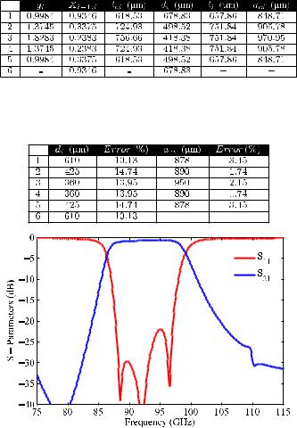
This procedure has been used to design a filter with an operation bandwidth from 87 to 98 GHz and the passband ripples of 0.005 dB. Ferro A6M LTCC sheets with the dielectric constant of 6.21 and thickness of 93.98 μm have been utilized. An initial width of 960 μm has been chosen for the first and last sections of the V-LIW filter to be consistent with the one in V-LIW transition for W-band. Table III includes all parameters have been calculated following steps in the design procedure.
The designed filter is then simulated and optimized using ANSYS HFSS. The optimized values of V-LIW width and iris’ opening length along with associated errors are listed in Table IV. It should be noted that the error in the calculation of di is mainly due to the fact that (12) has been found for discontinuities between cavities with identical width; on the other hand, in our case, as we discussed earlier, we have modified the width of V-LIW. Fig. 32 shows the simulation results of optimized W-band filter.
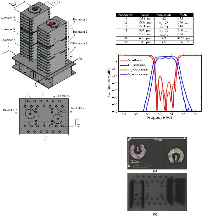
2) Ninth-Order V-Band Chebyshev Filter: The previous filter shows the excellent performance of V-LIW in filter design; however, this configuration is not suitable to be integrated with other components of a communication circuit. In a new model, we combine the proposed transitions in Section III and the iris openings that have also been used in W-band filter to realize a filter with coplanar inputs in the same plane. Fig. 33 depicts the proposed filter. This filter has four sections: 1) CPW-to-V-LIW transitions; 2) V-LIW sections; 3) V-LIW-to-H-LIW transition; and 4) H-LIW section. The iris
Fig. 32. Simulation results of W-band V-LIW fifth-order filter.
openings and inductive posts are located in V-LIW and H-LIW sections, respectively, to form cavity resonators. Therefore, the transition sections are also used as resonators, which lead to having a more compact design.
The drawback of this new structure is, we achieve a more convenient design for integration, at the expense of a more complicated structure which makes almost impossible to provide a fully analytical design procedure. To find an acceptable starting point for optimization, one can follow the previous design procedure with certain considerations given in the following.
1)In the first (and last) resonator, the designed transition from CPW to V-LIW should be added. Then, the position of this transition in the XY plane and also the aperture diameter where the signal via comes into the V- LIW have to be adjusted to provide the external quality factor (Qext) and coupling factor (k) given by [53]
Qext in = |
g0g1 f0 |
|
(14) |
BW |
|||
Qext out = |
gn gn+1 f0 |
(15) |
|
BW |
|||
880 |
IEEE TRANSACTIONS ON MICROWAVE THEORY AND TECHNIQUES, VOL. 67, NO. 3, MARCH 2019 |
TABLE V
PARAMETERS OF V-BAND V-LIW NINTH-ORDER FILTER
Fig. 34. Simulation and measurement results for V-band V-LIW filter.
Fig. 33. Geometry of ninth-order V-LIW filter. The green parts are iris discontinuities. (a) 3-D view. (b) Section cut at AA.
ki,i+1 |
= f0 |
|
g0gi+1 |
(16) |
||
|
|
BW |
1 |
|
|
|
where BW is the bandwidth and f0 is the center frequency corresponding to mid-band guided wavelength found by (8). The external quality factor for these resonators can be extracted from ANSYS HFSS simulation in association with MATLAB code. This code has been written by the authors based on [54].
2)For the second transition, between V-LIW and H-LIW, like the first transition, with adjusting the lateral position of transition and the aperture diameter, the desired coupling between the third and fourth resonators can be achieved. It should be noted that the lengths of these cavities have to be optimized at the same time to keep the resonance frequency of the coupled resonators unchanged.
3)Two inductive posts are used to realize the coupling between the fourth and fifth resonators. The distance between these two posts determines the level of coupling. This distance can be estimated by (12) and then applying the formula for effective width of SIW, presented in [55].
Applying the presented method, we have designed and optimized a filter for unlicensed 60-GHz applications. The filter is targeted at 58–62 GHz with passband ripples of
Fig. 35. Fabricated V-band V-LIW filter. (a) Top-view photograph. (b) X-ray photograph of inside of LTCC filter.
0.005 dB. The filter has been designed following the analytical procedure presented in the previous part of this section, and then the steps, presented here, carried out one by one to have a fast and accurate optimization. Dupont 9k7 LTCC tapes with a permittivity of 7.1 are used to realize the desired filter. The LIW width in both sections, V-LIW and H-LIW, is 1428 μm. Table V includes the optimized dimensions for the proposed filter; the dimensions that are not listed in this table can be found from either symmetry of the filter or dimensions for the transitions presented in the previous sections.
ISAPOUR AND KOUKI: V-LIW AND TRANSITIONS FOR mm-WAVE APPLICATIONS |
881 |
Fig. 34 shows the simulation and fabrication of the V-LIW V-band filter. As it can be seen in this figure, the results are in good agreement. The measured filter has a return loss of better than 15 dB over the entire unlicensed band and an insertion loss of 2.1 dB at 60 GHz. A photograph of the fabricated filter and an X-ray photograph of inside LTCC are illustrated in Fig. 35.
V. CONCLUSION
In this paper, we proposed a new guiding structure, named V-LIW, for multilayer fabrication technologies. The proposed transmission line allows us to integrate the passive components in the perpendicular direction to the surface. The characteristics of V-LIW are fully presented, and three different transitions have also been proposed to interconnect this line to the standard rectangular waveguides, coplanar waveguides, and conventional horizontal SIW. Furthermore, the superior capabilities of V-LIW for designing compact 3-D circuits have been demonstrated through designing different elementary components: two filters, T-junction power divider, and a coupler. The transitions, as well as the 3-D circuits, are successfully fabricated and measured in LTCC. The authors envision that the proposed V-LIW to be an excellent candidate for the mmwave compact 3-D circuits, where highly integrated low-loss structures are desired.
REFERENCES
[1]D. Deslandes and K. Wu, “Integrated microstrip and rectangular waveguide in planar form,” IEEE Microw. Wireless Compon. Lett., vol. 11, no. 2, pp. 68–70, Feb. 2001.
[2] Y. Cassivi, L. Perregrini, P. Arcioni, M. Bressan, K. Wu, and G. Conciauro, “Dispersion characteristics of substrate integrated rectangular waveguide,” IEEE Microw. Wireless Compon. Lett., vol. 12, no. 9,
pp.333–335, Sep. 2002.
[3]D. Deslandes and K. Wu, “Accurate modeling, wave mechanisms, and design considerations of a substrate integrated waveguide,” IEEE Trans. Microw. Theory Techn., vol. 54, no. 6, pp. 2516–2526, Jun. 2006.
[4]A. Isapour and A. B. Kouki, “Empty LTCC integrated waveguide with compact transitions for ultra-low loss millimeter-wave applications,”
IEEE Microw. Wireless Compon. Lett., vol. 27, no. 2, pp. 144–146, Feb. 2017.
[5]W. Che, K. Deng, D. Wang, and Y. L. Chow, “Analytical equivalence between substrate-integrated waveguide and rectangular waveguide,” IET Microw. Antennas Propag., vol. 2, no. 1, pp. 35–41, 2008.
[6]T. Shahvirdi and A. Banai, “Applying contour integral method for analysis of substrate integrated waveguide filters,” in Proc. Medit. Microw. Symp. (MMS), 2010, pp. 418–421.
[7]X.-P. Cheng and K. Wu, “Substrate integrated waveguide cross-coupled filter with negative coupling structure,” IEEE Trans. Microw. Theory Techn., vol. 56, no. 1, pp. 142–149, Jan. 2008.
[8]Y. J. Cheng, W. Hong, and K. Wu, “Broadband self-compensating phase shifter combining delay line and equal-length unequal-width phaser,”
IEEE Trans. Microw. Theory Techn., vol. 58, no. 1, pp. 203–210, Jan. 2010.
[9]Y. J. Cheng, W. Hong, and K. Wu, “94 GHz substrate integrated monopulse antenna array,” IEEE Trans. Antennas Propag., vol. 60, no. 1,
pp.121–129, Jan. 2012.
[10]K. Wang, S.-W. Wong, G.-H. Sun, Z. N. Chen, L. Zhu, and Q.-X. Chu, “Synthesis method for substrate-integrated waveguide bandpass filter with even-order Chebyshev response,” IEEE Trans. Compon., Packag., Manuf. Technol., vol. 6, no. 1, pp. 126–135, Jan. 2016.
[11]Y. Li, L.-A. Yang, L. Du, K. Zhang, and Y. Hao, “Design of millimeterwave resonant cavity and filter using 3-D substrate-integrated circular waveguide,” IEEE Microw. Wireless Compon. Lett., vol. 27, no. 8,
pp.706–708, Aug. 2017.
[12]Q. Zhang and Y. Lu, “E-band ‘T’ shape transitions between substrate integrated waveguide and standard waveguide,” in Proc. Asia–Pacific Microw. Conf. (APMC), 2008, pp. 1–4.
[13]B. Y. El Khatib, T. Djerafi, and K. Wu, “Substrate-integrated waveguide vertical interconnects for 3-D integrated circuits,” IEEE Trans. Compon., Packag., Manuf. Technol., vol. 2, no. 9, pp. 1526–1535, Sep. 2012.
[14]A. Doghri, T. Djerafi, A. Ghiotto, and K. Wu, “Substrate integrated waveguide directional couplers for compact three-dimensional integrated circuits,” IEEE Trans. Microw. Theory Techn., vol. 63, no. 1,
pp.209–221, Jan. 2015.
[15]A. Doghri, A. Ghiotto, T. Djerafi, and K. Wu, “Compact and low cost substrate integrated waveguide cavity and bandpass filter using surface mount shorting stubs,” in IEEE MTT-S Int. Microw. Symp. Dig., Jun. 2012, pp. 1–3.
[16]A. Doghri, A. Ghiotto, T. Djerafi, and K. Wu, “Schwinger coupler for substrate integrated circuits and systems,” in Proc. Eur. Microw. Conf., Oct. 2013, pp. 306–309.
[17]A. Doghri, A. Ghiotto, T. Djerafi, and K. Wu, “Corrugated SIW L-folded antipodal parabolic tapered slot antenna,” in Proc. Asia Pacific Microw. Conf., Dec. 2012, pp. 893–895.
[18]Y. Huang, K.-L. Wu, and M. Ehlert, “An integrated LTCC laminated waveguide-to-microstrip line T-junction,” IEEE Microw. Wireless Compon. Lett., vol. 13, no. 8, pp. 338–339, Aug. 2003.
[19]I. Wolff, “Design and technology of microwave and millimeterwave LTCC circuits and systems,” in Proc. Int. Symp. Signals, Syst. Electron. (ISSSE), 2007, pp. 505–512.
[20]J. Heilala et al., “LTCC technology for cost-effective packaging of photonic modules,” Assembly Autom., vol. 25, no. 1, pp. 30–37, 2005.
[21]K.-I. Kim, J.-M. Kim, J.-M. Kim, G.-C. Hwang, C.-W. Baek, and Y.-K. Kim, “Packaging for RF MEMS devices using LTCC substrate and BCB adhesive layer,” J. Micromech. Microeng., vol. 16, no. 1, p. 150, 2005.
[22]B. Zhou, Q. Ma, Q. Wang, L. Yan, N. Zhou, and C.-H. Cheng, “Highly intergrated X-band LTCC receiver module,” Prog. Electromagn. Res. C, vol. 71, pp. 51–58, 2017.
[23]Y.-S. Lin, C.-C. Liu, K.-M. Li, and C. H. Chen, “Design of an LTCC tri-band transceiver module for GPRS mobile applications,” IEEE Trans. Microw. Theory Techn., vol. 52, no. 12, pp. 2718–2724, Dec. 2004.
[24]D. Deslandes and K. Wu, “Design consideration and performance analysis of substrate integrated waveguide components,” in Proc. 32nd Eur. Microw. Conf., 2002, pp. 1–4.
[25]F. Xu and K. Wu, “Guided-wave and leakage characteristics of substrate integrated waveguide,” IEEE Trans. Microw. Theory Techn., vol. 53, no. 1, pp. 66–73, Jan. 2005.
[26]S. C. Chapra, Applied Numerical Methods With MATLAB for Engineers and Scientists. New York, NY, USA: McGraw-Hill, 2005.
[27]D. M. Pozar, Microwave Engineering. Hoboken, NJ, USA: Wiley, 2009.
[28]D. F. Williams, “Rectangular-waveguide vector-network-analyzer calibrations with imperfect test ports,” in Proc. 76th ARFTG Microw. Meas. Symp. (ARFTG), 2010, pp. 1–8.
[29]G. Wheeler, “Broadband waveguide-to-coax transitions,” in Proc. IRE Int. Conv. Rec., New York, NY, USA, 1966, pp. 182–185.
[30]M. D. Deshpande, B. N. Das, and G. S. Sanyal, “Analysis of an end launcher for an X-band rectangular waveguide,” IEEE Trans. Microw. Theory Techn., vol. MTT-27, no. 8, pp. 731–735, Aug. 1979.
[31]S. M. Saad, “A more accurate analysis and design of coaxial-to- rectangular waveguide end launcher,” IEEE Trans. Microw. Theory Techn., vol. 38, no. 2, pp. 129–134, Feb. 1990.
[32]P. Wade. (Nov. 2006). Rectangular Waveguide to Coax Transition Design. [Online]. Available: http://www.w1ghz.org/QEX/ Rectangular_Waveguide_to_Coax_Transition_Design.pdf
[33]I. Fabregas, K. Shamsaifar, and J. M. Rebollar, “Coaxial to rectangular waveguide transitions,” in Antennas Propag. Soc. Int. Symp. (AP-S) Dig., URSI Radio Sci. Meeting Nucl. EMP Meeting, vol. 4, Jun. 1992,
pp.2122–2125.
[34]S. Mukherjee, P. Chongder, K. V. Srivastava, and A. Biswas, “Design of
abroadband coaxial to substrate integrated waveguide (SIW) transition,” in Proc. Asia–Pacific Microw. Conf. (APMC), Nov. 2013, pp. 896–898.
[35]D. Deslandes and K. Wu, “Analysis and design of current probe transition from grounded coplanar to substrate integrated rectangular waveguides,” IEEE Trans. Microw. Theory Techn., vol. 53, no. 8,
pp.2487–2494, Aug. 2005.
[36]A. Singh and S. Verma, Fundamentals of Microwave Engineering: Principles, Waveguides, Microwave Amplifiers and Applications. New Delhi, India: PHI Learning, 2009. [Online]. Available: https://www. phindia.com/Books/BookDetail/OTc4LTgxLTIwMy0zNzE2LTk

882 |
IEEE TRANSACTIONS ON MICROWAVE THEORY AND TECHNIQUES, VOL. 67, NO. 3, MARCH 2019 |
[37]W. W. Mumford, “The optimum piston position for wide-band coaxial- to-waveguide transducers,” Proc. IRE, vol. 41, no. 2, pp. 256–261, Feb. 1953.
[38]S. Yang and A. E. Fathy, “Design equations of arbitrary power split ratio waveguide T-junctions using a curve fitting approach,” Int. J. RF Microw. Comput.-Aided Eng., vol. 19, no. 1, pp. 91–98, 2009.
[39]J. Hirokawa, K. Sakurai, M. Ando, and N. Goto, “An analysis of a waveguide T junction with an inductive post,” IEEE Trans. Microw. Theory Techn., vol. 39, no. 3, pp. 563–566, Mar. 1991.
[40]S. Germain, D. Deslandes, and K. Wu, “Development of substrate integrated waveguide power dividers,” in Proc. Can. Conf. Elect. Comput. Eng. (CCECE), vol. 3, 2003, pp. 1921–1924.
[41]F. Parment, A. Ghiotto, T. P. Vuong, J. M. Duchamp, and K. Wu, “Air-filled substrate integrated waveguide for low-loss and high powerhandling millimeter-wave substrate integrated circuits,” IEEE Trans. Microw. Theory Techn., vol. 63, no. 4, pp. 1228–1238, Apr. 2015.
[42]C. G. Montgomery, R. H. Dicke, and E. M. Purcell, Eds., Principles of Microwave Circuits. Edison, NJ, USA: IET, 1948.
[43] D. Dancila, X. Rottenberg, H. A. C. Tilmans, W. De Raedt, and I. Huynen, “57–64 GHz seven-pole bandpass filter substrate integrated waveguide (SIW) in LTCC,” in Proc. IEEE MTT-S Int. Microw. Workshop Ser. Millim. Wave Integr. Technol., Sep. 2011, pp. 200–203.
[44]D. Deslandes and K. Wu, “Single-substrate integration technique of planar circuits and waveguide filters,” IEEE Trans. Microw. Theory Techn., vol. 51, no. 2, pp. 593–596, Feb. 2003.
[45]S. T. Choi, K. S. Yang, K. Tokuda, and Y. H. Kim, “A V-band planar narrow bandpass filter using a new type integrated waveguide transition,”
IEEE Microw. Wireless Compon. Lett., vol. 14, no. 12, pp. 545–547, Dec. 2004.
[46]D. Deslandes and K. Wu, “Millimeter-wave substrate integrated waveguide filters,” in Proc. Can. Conf. Elect. Comput. Eng. Toward Caring Humane Technol. (CCECE), vol. 3, May 2003, pp. 1917–1920.
[47]T.-S. Yun, H. Nam, K.-B. Kim, and J.-C. Lee, “Iris waveguide bandpass filter using substrate integrated waveguide (SIW) for satellite communication,” in Proc. Asia–Pacific Microw. Conf., vol. 1, Dec. 2005, p. 4.
[48]X. P. Chen and K. Wu, “Substrate integrated waveguide cross-coupled filter with negative coupling structure,” IEEE Trans. Microw. Theory Techn., vol. 56, no. 1, pp. 142–149, Jan. 2008.
[49]Z. C. Hao, W. Hong, X. P. Chen, J. X. Chen, K. Wu, and T. J. Cui, “Multilayered substrate integrated waveguide (MSIW) elliptic filter,”
IEEE Microw. Wireless Compon. Lett., vol. 15, no. 2, pp. 95–97, Feb. 2005.
[50]L. Q. Bui, D. Ball, and T. Itoh, “Broad-band millimeter-wave E-plane bandpass filters (short papers),” IEEE Trans. Microw. Theory Techn., vol. MTT-32, no. 12, pp. 1655–1658, Dec. 1984.
[51]S. B. Cohn, “Direct-coupled-resonator filters,” Proc. IRE, vol. 45, no. 2, pp. 187–196, Feb. 1957.
[52]N. Marcuvitz, Waveguide Handbook, vol. 21. Edison, NJ, USA: IET, 1951.
[53]L. Harle, “Microwave micromachined cavity filters,” Ph.D. dissertation, Dept. Elect. Eng., Univ. Michigan, Ann Arbor, MI, USA, 2003.
[54]D. Kajfez, Q-Factor. Hoboken, NJ, USA: Wiley, 2005.
[55]F. Xu and K. Wu, “Guided-wave and leakage characteristics of substrate integrated waveguide,” IEEE Trans. Microw. Theory Techn., vol. 53, no. 1, pp. 66–73, Jan. 2005.
Aria Isapour (GS’13) received the B.Sc. degree in electrical engineering from the Iran University of Science and Technology, Tehran, Iran, in 2009, the M.Sc. degree in electrical engineering from the Sharif University of Technology, Tehran, in 2011, and the Ph.D. degree in electrical engineering from the École de Technologie Supérieure, Montréal, QC, Canada, in 2018.
He is currently a Staff RF Designer with the Infinera Corporation, Ottawa, ON, Canada. His current research interests include passive microwave
and millimeter-wave circuits, signal integrity, and low-temperature cofired ceramics for 3-D passive circuits and packaging.
Ammar Kouki (S’88–M’92–SM’01) received the B.S. (Hons.) and M.S. degrees in engineering science from Pennsylvania State University, State College, PA, USA, in 1985 and 1987, respectively, and the Ph.D. degree in electrical engineering from the University of Illinois at Urbana–Champaign, Champaign, IL, USA, in 1991.
He |
is currently a |
Full |
Professor |
of electri- |
cal |
engineering and |
the |
Founding |
Director of |
the LTCC@ETS Laboratory, École de Technologie Supérieure, Montréal, QC, Canada. His current research interests include active and passive microwave and millimeter-wave
devices and circuits, intelligent and efficient RF front ends, 3-D circuits in lowtemperature cofired ceramics, applied computational electromagnetics, and antennas radio-wave propagation modeling.