

диафрагмированные волноводные фильтры / b0603d30-ec11-4335-9f54-7d8b96fc6793
.pdf134 |
IEEE TRANSACTIONS ON ANTENNAS AND PROPAGATION, VOL. 61, NO. 1, JANUARY 2013 |
Applying Band-Pass Filter Techniques to the Design of Small-Aperture Evanescent-Mode Waveguide Antennas
Peter Ludlow, Vincent Fusco, Fellow, IEEE, George Goussetis, Member, IEEE, and
Dmitry E. Zelenchuk, Member, IEEE
Abstract—A design methodology is presented which applies band-pass filter principles to form wideband small-aperture evanescent-mode waveguide antenna designs. This approach permits matching of the complex antenna aperture admittance of an evanescent-mode open-ended waveguide to a real impedance generator, and thereby to an SMA coaxial feeding probe. A reflection coefficient of less than 10 dB was obtained over a measured bandwidth of 15%, from 2.30–2.68 GHz, in 2.72 GHz cutoff waveguide. Capacitive posts and evanescent-mode waveguide sections are used to form the resonators/coupling elements of the antenna’s filtering sections. Measured realised gain variation from 3.5–4.7 dBi is observed across the bandwidth. The antenna’s maximum aperture dimension is 


 at the upper frequency in the bandwidth and so it is suitable for use in a wide angle scanning phased array.
Index Terms—Electrically small aperture, evanescent waveguide, filtering antenna, phased arrays.
I. INTRODUCTION
P HASED arrays are a well-established technique to produce steerable directive beams [1]–[3]. Waveguide or cavity type radiators are particularly suitable for applications that call for medium to high power handling as well as highly isolated array elements (e.g. for wide angle scanning). Despite these favourable characteristics, waveguide and cavity radiators for practical phased array systems suffer from limited bandwidth and/or large geometrical dimensions. On one hand, apertures of propagating waveguides involve dimensions of the order of greater than a half wavelength, which in a phased array arrangement leads to unwanted grating lobes; this becomes increasingly significant as the operating frequency shifts higher with respect to the waveguide cutoff, hence posing additional constraints to the available bandwidth. On the other hand, the impedance of unmodified waveguide apertures exhibits a strong reactive impedance [4], hence matching is not trivial, particularly over a broad bandwidth. Although flaring the waveguide can improve matching, this increases the footprint
Manuscript received October 19, 2011; revised February 08, 2012; accepted September 18, 2012. Date of publication September 21, 2012; date of current version December 28, 2012. This work was supported by the UK Engineering and Physical Science Research Council under Grant EP/E01707X/1 The work of P. Ludlow was supported by Powerwave Technologies and by the Department of Learning (DEL) for Northern Ireland.
The authors are with The Institute of Electronics, Communications and Information Technology, Queen’s University Belfast, Queen’s Island, Belfast BT3 9DT, Northern Ireland, U.K. (e-mail: v.fusco@ecit.qub.ac.uk).
Digital Object Identifier 10.1109/TAP.2012.2220314
and hence is not suitable for phased arrays. Cavity radiators similarly suffer from narrow bandwidth stemming from their resonant operation.
Evanescent-mode open-ended waveguide radiators are formed from an open-ended waveguide that is operated below its cutoff frequency and are therefore more compact electrically than above-cutoff open-ended waveguide antennas. Although this feature can alleviate the limitations associated with the emergence of grating lobes in a phased array, the electromagnetic fields in an evanescent-mode waveguide are reactive and decay exponentially; hence the excitation of the open-ended aperture over a substantial bandwidth remains a significant challenge.
Open-ended waveguide antennas with aperture dimensions 


 may be dielectric-filled to enable propagation [5]–[8].
The designs of [5], [6] use waveguide with 


 dielectric
filling and an evanescent-mode air gap at a distance from the aperture to match from the waveguide’s characteristic impedance to free space. In [5] an 8% bandwidth for reflection
coefficient |
|
|
|
|
|
|
10 dB is reported, with aperture dimensions |
||||||||||||||||||||||||||||||||||
|
|
|
|
|
|
|
|
|
|
|
|
|
|
|
|
|
across the bandwidth. Reference [6] reports |
||||||||||||||||||||||||
|
|
|
|
|
|
|
|
|
|
|
|
|
|
|
|||||||||||||||||||||||||||
a 15% bandwidth for reflection coefficient |
|
|
|
10 dB, with |
|||||||||||||||||||||||||||||||||||||
aperture dimensions |
|
|
|
|
|
|
|
|
|
|
|
|
|
|
|
|
|
|
|
across the bandwidth. |
|||||||||||||||||||||
|
|
|
|
|
|
|
|||||||||||||||||||||||||||||||||||
|
|
|
|
|
|
|
|
|
|
|
|
|
|||||||||||||||||||||||||||||
|
|
|
|
|
|
|
|
|
|
|
|
|
|
|
|
|
|
|
|
|
|
|
|
|
|
|
|
|
|
|
|
|
|
|
|
|
|
|
|
|
|
The design technique of [7] uses partially dielectric loaded rectangular waveguides—whereby the centre of the waveguide is air-filled and allows propagation of a pseudo-TEM wave—to achieve antenna designs that have aperture dimensions equal to 


 and
and 


 at the operating frequency,
for 10 dB reflection coefficient bandwidths of 0.65% and 1.2%, respectively.
In [9], a rectangular evanescent-mode waveguide aperture is matched to free space through loading of the waveguide with double ring resonators printed on to an E-plane oriented dielectric substrate that is centred in the waveguide. The design exploits the principle that backward wave propagation in an evanescent-mode waveguide is possible if the waveguide is loaded in such a way that the effective permeability in the transversal direction of the waveguide is negative. A bandwidth
of 5% for reflection coefficient |
|
|
|
|
|
|
|
10 dB is reported with |
||||||||||||||||
aperture dimensions |
|
|
|
|
|
|
|
|
|
|
|
|
|
|
|
|
|
|
|
|
|
|
across the bandwidth |
|
|
|
|
|
|
|
|
|
|
|
|
|
|
|
|
|
|
|
|
|
|
||||
and antenna length |
|
|
|
|
|
|
|
. |
|
|
|
|
|
|
|
|
|
|
|
|
|
|
|
|
|
|
|
|
|
|
|
|
|
|
|
|
|
|
|
|
|
|
|
|
|||||
|
|
|
|
|
|
|
|
|
|
|
|
|
|
|
|
|
|
|
|
|
||||
|
|
|
|
|
|
|
|
|
|
|
|
|
|
|
|
|
|
|
|
|
|
|
|
|
In [8], [10], [11] loading of the waveguide aperture, with protruding dielectric [8] or variable width strips [10], [11], is used along with more complex feeding arrangements to enable wideband waveguide matching to free space. Reference [8] proposes exciting a dielectric-filled waveguide using an L-shaped feed,
0018-926X/$31.00 © 2012 British Crown Copyright
LUDLOW et al.: APPLYING BAND-PASS FILTER TECHNIQUES TO THE DESIGN OF SMALL-APERTURE EVANESCENT-MODE WAVEGUIDE ANTENNAS |
135 |
whereby the dielectric (which has 


 ) protrudes in a con- ical-shape from the aperture. A match over a 27% bandwidth is achieved, for aperture width/height


 across the band-
width. In [10], [11], square evanescent-mode waveguide phased array antennas are presented that are impedance matched to free space through using near-fed coaxial probes that resonate variable width strips placed across the aperture, with a dielectric sheet air-spaced from the aperture to permit wide-angle scan-
ning; bandwidths of 42% for reflection coefficient |
|
|
|
|
6 dB |
|||
and 69% bandwidth for a typical reflection coefficient of |
|
|
|
|
7 |
|||
dB are reported, respectively. |
|
|
|
|
||||
The Imaginary Smith Chart was used in [12], [13] to design a narrowband match to the aperture admittance of an evanes- cent-mode open-ended waveguide. In [12] this resulted in a narrowband antenna design with a simulated bandwidth of 3.2% for reflection coefficient 
 10 dB and a maximum realised gain
of 3.71 dBi. Here a capacitive post and a length of evanescentmode waveguide were used to achieve the desired matching, with the structure 


 in size across the bandwidth. In
[13] a reconfigurable evanescent-mode open-ended waveguide antenna was presented that permitted tuning of reflection coefficient at the coaxial input port across an operating frequency range of 19.4%, with a maximum realised gain of 5 dBi and the maximum dimension of the antenna 


 . This is achieved
through the use of a printed iris with a shunt varactor diode connected across the aperture of the waveguide and a length of evanescent-mode waveguide.
In this paper a new design technique is outlined that enables matching to the aperture admittance of an evanescent-mode open-ended waveguide antenna, and thereby to free space. The proposed technique is based on well-established evanes- cent-mode waveguide filter theory [14] and is therefore efficient and may be readily applied to higher order designs. The iterative design technique is very straightforward and allows the design parameters to be established without extensive electromagnetic simulation. Moreover, the proposed scheme dispenses the need for dielectric blocks, as used in [5]–[8], which can be costly and/or add mass, or other protruding elements, as used in [10], [11]. Furthermore, the feeding arrangement used is much simpler than that of [8], [10], [11] as a standard SMA coaxial feed inserted through the broad wall of the waveguide is used to excite the antenna. The structure of the paper is as follows. In Section II, a detailed design procedure is derived for a wideband antenna design in evanescent-mode waveguide that uses band-pass filter techniques with 

 resonators
to achieve the wideband match. In Section III, a match at 2.4 GHz to a rectangular waveguide aperture with 


 is
is
designed using this procedure, using the circuit-based simulator, ADS [15], and electromagnetic simulator, CST [16]. The measured input matching and farfield results are then presented in Section IV and compared with simulated results.
II. DESIGN PROCEDURE FOR A WIDEBAND SMALL-APERTURE
EVANESCENT-MODE WAVEGUIDE ANTENNA
According to the proposed method the antenna is designed such that the radiating antenna aperture forms the last resonator and the load resistance/conductance of the filter circuit. If a load to be matched has a reactive part, perfect power transmission to
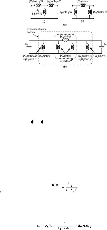
Fig. 1. (a) (i) T and (ii)  equivalent lumped circuit models for an evanescentmode waveguide section (


 and
and 


 ) (b) Evanescent-mode waveguide filter model [14].
the load is possible only at discrete frequencies, and not over a band of frequencies [17]. Furthermore, it will usually be found that the overall transmission can be improved if at least a small amount of power is reflected at all frequencies [17]. It is convenient to characterize the complex load to be matched by its decrement, which is defined in [17] as:
where |
|
|
|
|
|
|
|
|
|
|
|
|
|
|
|
|
|
|
|
|
|
|
(1) |
|
|
|
|
|
|
|
|
|
|
|
|
|
|
|
|
|
|
|
|
|
|
|
|
|
|
|
of the resonant load. |
||||||||||||||||||||
For TE evanescent modes, T or  circuits may be used as an equivalent lumped circuit model of a section of waveguide, as shown in Fig. 1(a). The approximation to lumped circuits becomes closer as the frequency of operation moves further below cutoff, with exact correspondence established sufficiently far below the cutoff frequency [18]. A correction factor,
  , is derived in [14] to account for the deviation in the frequency dependencies of the evanescent-mode waveguide elements and the equivalent lumped elements; while the resonator slope parameters of the lumped resonator equivalents have a pole at infinite frequency, the evanescent-mode waveguide elements will have a pole at the cutoff frequency of the waveguide and therefore, especially for frequencies closer to cutoff, the resonator slope will be greater than for the lumped equivalent.
(2)
By manipulation of the  equivalent circuit model such that negative shunt elements of equal magnitude to the series element are introduced [14], an admittance inverter can be formed, as shown in Fig. 1(b). Such an inverter is only possible if the shunt inductive elements in Fig. 1(b) add up algebraically to the original value in Fig. 1(a)(ii). Using the resonance condition, the required shunt capacitance values can be found from:
(3) |
The value of each resonator therefore depends on the length of the adjacent evanescent-mode waveguide sections and how
136 |
IEEE TRANSACTIONS ON ANTENNAS AND PROPAGATION, VOL. 61, NO. 1, JANUARY 2013 |
far the operating frequency is below cutoff (which in turn determines the values of 
 and
and  ). The value of each J-inverter is determined by:
(4)
The J-inverter values are therefore also determined by the length of evanescent-mode waveguide used and how far the operating frequency is below cutoff.
According to the theory presented in [17], the value of each inverter depends on the value of the slope parameters of the adjacent resonators that are coupled by the inverter, with the first and last J-inverters enabling matching to source and load resistances of a specified value at each side of the filter. In a distributed coupled resonator filter, for instance, the resonator slope parameters are often chosen to be of a convenient value, e.g. by using transmission line of 

 in length as resonators—the value of J-inverters required may therefore be easily determined. However it is not possible in this case to arbitrarily select resonator parameters and then design J-inverters based on these values since both J-inverter and resonator slope parameters depend on the length of each evanescent-mode waveguide section. The value of each J-inverter and resonator therefore have to be co-designed—an iterative design process is described in [18] for narrow to moderate bandwidths.
In the filtering antennas presented in [19], [20] an n-pole filter is firstly designed, using propagating waveguide sections that are coupled by capacitive or inductive irises; a radiating slot antenna element is then built on or inside the nth resonator and the distance to the nth coupling element adjusted as required. Note that the slot antenna elements used in [19], [20] have a bandwidth equal to or greater than that of the filter section, with the main drive of the work in each case being compact integration of filter and antenna. In the evanescent-mode waveguide antenna outlined here band-pass filter techniques are instead applied to enable wideband antenna design in evanescent-mode waveguide.
The difficulty in achieving this is that the coupling element and resonator values in evanescent-mode waveguide filters are interdependent as outlined above and an iterative procedure is therefore necessary, since changing the nth resonator will affect the nth coupling element and thereby the (n-1)th resonator etc. The use of an iterative technique in the design hence enables wideband antenna design in evanescent-mode waveguide, which has smaller transverse dimensions than unmodified propagating waveguide and may therefore be used in a wide-angle scanning phased array.
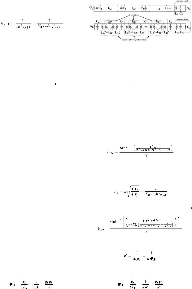
Modification of the theory outlined in [14] and [18] had to be made to accommodate matching to the complex shunt load represented by the aperture of an evanescent-mode open-ended waveguide antenna. A band-pass filter circuit in evanescentmode waveguide that matches to a shunt resonant antenna load is as shown in Fig. 2 for a filter with order 

 and will be used in the remainder of this section to illustrate the proposed synthesis procedure.
The Q factor of the load has to meet the following criterion [17]:
(5)
Fig. 2. Evanescent-mode waveguide filter with 

 that uses J-inverter coupled resonators matched to a shunt resonant antenna load.
|
|
For a particular value of |
|
the |
|
values that minimise the |
||||||||||||||||||||||||||||||
|
|
|||||||||||||||||||||||||||||||||||
value of |
|
|
|
|
|
|
|
|
|
|
|
|
|
|
are given in [17]. |
|
To ensure a reflection coef- |
|||||||||||||||||||
|
|
|
|
|
||||||||||||||||||||||||||||||||
ficient |
|
|
|
|
|
|
10 |
|
|
dB across the band a maximum value of insertion |
||||||||||||||||||||||||||
loss, |
|
|
|
|
|
|
|
|
|
|
|
, of 0.46 dB is required. For a filter circuit with |
||||||||||||||||||||||||
|
|
|
|
|
|
|
|
|
|
|
||||||||||||||||||||||||||
|
|
|
|
|
this |
|
requires |
|
|
|
|
|
|
|
|
|
|
[17]. |
|
|||||||||||||||||
|
|
The value of |
|
|
|
in (5) incorporates the inductive resonator |
||||||||||||||||||||||||||||||
|
|
|
||||||||||||||||||||||||||||||||||
|
|
|
|
|
||||||||||||||||||||||||||||||||
|
|
|
|
|
|
|
|
|
|
|
|
|
|
|
|
|
|
|
|
|
|
|
|
|
|
|
|
|
|
|
|
|
|
|
|
|
component of the adjacent evanescent-mode waveguide section,
|
|
|
, shunt capacitance |
|
|
|
, and the reactive elements of the an- |
||||||||||||||||||||||||||||||||||||||||||||||||||
|
|
|
|
|
|||||||||||||||||||||||||||||||||||||||||||||||||||||
|
|
|
|
|
|
||||||||||||||||||||||||||||||||||||||||||||||||||||
tenna load, |
|
|
|
and |
|
|
|
. Note that the correction factor, |
|
, has |
|||||||||||||||||||||||||||||||||||||||||||||||
|
|
|
|
|
|
||||||||||||||||||||||||||||||||||||||||||||||||||||
|
|
|
|
||||||||||||||||||||||||||||||||||||||||||||||||||||||
to be used when the reactance of |
|
|
|
|
|
|
is used. |
|
|
|
|
is therefore |
|||||||||||||||||||||||||||||||||||||||||||||
|
|
|
|
|
|
|
|||||||||||||||||||||||||||||||||||||||||||||||||||
|
|
|
|
|
|
|
|
|
|||||||||||||||||||||||||||||||||||||||||||||||||
equal to: |
|
|
|
|
|
|
|
|
|
|
|
|
|
|
|
|
|
|
|
|
|
|
|
|
|
|
|
|
|
|
|
|
|
|
|
|
|
|
|
|
|
|
|
|
|
|
|
(6) |
|||||||||
|
|
|
|
|
|
|
|
|
|
|
|
|
|
|
|
|
|
|
|
|
|
|
|
|
|
|
|
|
|
|
|
|
|
|
|
|
|
|
|
|
|
|
|
|
|
|
|
|
|
|
|
|
|
||||
|
|
|
|
|
|
|
|
|
|
|
|
|
|
|
|
|
|
|
|
|
|
|
|
|
|
|
|
|
|
|
|
|
|
|
|
|
|
|
|
|
|
|
|
|
|
|
|
|
|
|
|
|
|
|
|||
By combining (5) and (6) it is possible to derive an expression for 

 that allows the quality factor for the load to meet the criterion given in (5):
(7)
However there is a further criterion that has to be met with regard to 

 —the value of the J-inverter,
 , is defined by

 , as shown in (4); however
 also has to meet the criterion for a J-inverter used to couple two resonators in a band-pass filter circuit:
(8)
By manipulating (8) it is possible to derive a second expression for 

 ; note that the expression for
 uses the value of

 derived above:
(9)
The load decrement,  , was defined in (1) as being the reciprocal of the product


 ; similarly, a source decrement,
 , may also be defined, which for an

 filter equals:
(10)
On the source side of the filter the quality factor for the source has to satisfy the following criterion to give reflection coefficient 
 10 dB across the bandwidth:
(11)
LUDLOW et al.: APPLYING BAND-PASS FILTER TECHNIQUES TO THE DESIGN OF SMALL-APERTURE EVANESCENT-MODE WAVEGUIDE ANTENNAS |
137 |
It is now possible to derive an expression for 

 that allows the quality factor of the source to meet the criterion stated in (11):
(12)
However there is a further criterion that has to be met with regard to 

 —by manipulating (8) it is possible to derive an expression for


 ; note that the expression for
 uses the value of


 derived above:
(13)
To ensure that matching is as desired for the filter design it is essential that 


 and
and 


 , in order to ensure that the criteria stated in (5) and (11) are satisfied. The terms that may be varied in (7), (9), (12) and (13) are
 ,
, 
 ,
,  and
and 
 . The remaining terms in each expression can then be fixed using: (i) the centre frequency,
 (ii) the parameters of the antenna load,
 ,
, 
 ,
,  (iii) the
 values for the value of
  defined by the load (iv) the parameters of the evanescent-mode waveguide at the centre frequency i.e. characteristic reactance,
 , correction factor for the resonators,
  , and propagation constant,
  , which is defined according to the waveguide width,
  , for the definition of characteristic impedance used here, i.e. wave impedance.
As a starting point for the iteration, values of 
 and
and 
 are input to (9) and (13), with the values of
  and
and 
 adjusted until


 and
and 


 . This allows lengths of evanes- cent-mode waveguide

 and
and 

 to be derived that will satisfy
the matching requirements for particular values of 
 and
and 
 . However, a further step in the iteration is now required since the values of
 and
and 
 are also dependent on the centre inverter,

 . An expression for

 may be derived using (8) that will allow
 to be of the value required by the filter design. Note that the values for
 and
and 
 defined at the beginning of the iteration are used in the expression for

 .
.
(14)
The iterated value of 
 ,
, 
 , may therefore be written as follows, with the value of

 given by


 and the value of

 given by (18):
The design process for a wideband small-aperture evanes- cent-mode open-ended waveguide antenna that uses a band-pass filter matching network of order 

 may therefore be summarized as follows:
i.Define waveguide height/width, 

 , and the centre frequency,
  , at which the antenna design is to operate.
ii.Calculate the characteristic reactance, 
 , correction factor for the resonators,
  , and propagation constant,
  for these waveguide dimensions at the centre frequency.
iii.For the given waveguide dimensions evaluate the aperture admittance characteristics around this frequency and define an equivalent 


 circuit.
iv.Define the reflection coefficient that is required over the band and from [17] find the value of the load decrement,  , required and thereby the
 values for the filter design.
v.Define values of 
 and
and 
 and find values of
 and
and 
that satisfy (7), (9), (12) and (13) such that 

 and
and 


 .
.
vi.Input these values of 
 and
and 
 and
and 


 into (14)–(16) and determine


 and
and 


 .
.
vii.Repeat steps (v)–(vi) with different starting values of 
 and
and 
 , which may be higher or lower than the previous ones depending on the values of


 and
and 


 calculated in step (vi), with the aim that both converge to unity, i.e. if


 is
is  1 then a higher starting value of

 should be chosen and vice versa, similarly for
 . The convergence criteria for the synthesis procedure is therefore that


 ,
, 


 ,
, 


 ,
, 


 . Once the iteration process is complete, the values of lengths

 ,
, 

 and
and 

 are then known (from (7), (9), (14) and (12), (13) respectively). The value of required shunt capacitances is given by:
(17)
(18)
(19)
(20)
The value of 
 is determined by the iteration and so cannot be freely chosen; from design experience its value is generally one-quarter to half of the value of
 . From (7) and (12) it is possible to define maximum bounds for the bandwidth,
  , over which the load may be matched for the reflection coefficient desired, since


 . From (7):
|
|
|
|
|
|
|
|
|
|
|
|
|
|
|
|
|
|
|
|
|
|
|
|
|
|
|
|
|
|
|
|
|
|
|
|
|
|
|
|
|
|
|
|
|
|
|
|
|
|
|
|
|
|
|
|
|
|
|
|
|
|
|
|
|
|
|
|
|
|
|
|
|
|
|
|
|
|
|
|
|
|
|
|
|
|
|
|
|
|
|
|
|
|
|
|
|
|
|
|
|
|
|
(21) |
|
|
|
|
|
|
|
|
|
|
|
|
|
|
|
|
|
|
|
|
|
|
|
|
|
|
|
|
|
|
|
|
|
|
|
|
|
|
|
|
|
|
|
|
|
(15) |
|
|
|
|
|
|
|
|
|
|
|
|
|
|
|
|
|
|
|
|
|
|
|
|
|
|
|
|
|
|
|
|
|
|
|
|
|
|
|
|
|
|||||||||||||||||
The iterated value of |
|
|
|
, |
|
|
|
, may be defined as follows, with From (12): |
|||||||||||||||||||||||||||||||||||||||||||||||||||||||||||||||||||||||||||||||||||||||||||||||
|
|
|
|
|
|
||||||||||||||||||||||||||||||||||||||||||||||||||||||||||||||||||||||||||||||||||||||||||||||||||
the value of |
|
|
given by |
|
|
|
|
|
|
|
|
: |
|
|
|
|
|
|
|
|
|
|
|
|
|
|
|
|
|
|
|
|
|
|
|
|
|
|
|
|
|
|
|
|
|
|
|
|
|
|
|
|
|
|
|
|
|
|
|
|
|
|
|
|
|
|
|
|
|
|
|
|
|
|
|
|
|
|
|
|
|
|
|
|
|
|
(22) |
||||||||||||||||
|
|
|
|
|
|
|
|
|
|
|
|
|
|
|
|
|
|
|
|
|
|
|
|
|
|
|
|
|
|
|
|
|
|
|
|
|
|
|
|
|
|
|
|
|
|
|
|
|
|
|
|
|
|
|
|
|
|
|
|
|
|
|
|
|
|
|
|
|
|
|
|
|
|
|
|
|
|
|
|
|
|
||||||||||||||||||||||
|
|
|
|
|
|
|
|
|
|
|
|
|
|
|
|
|
|
|
|
|
|
|
|
|
|
|
|
|
|
|
|
|
|
|
|
|
|
|
|
|
|
|
|
|
|
|
|
|
|
|
|
|
|
|
|
|
|
|
|
|
|
|
|
|
|
|
|
|
|
|
|
|
|
|
|
|
|
|
|
|
|
|
|
|
|||||||||||||||||||
|
|
|
|
|
|
|
|
|
|
|
|
|
|
|
|
|
|
|
|
|
|
|
|
|
|
|
|
|
|
|
|
|
|
|
|
|
|
|
|
|
|
|
|
|
|
|
|
|
|
|
|
|
|
|
|
|
|
|
|
|
|
|
|
|
|
|
|
|
|
|
|
|
|
|
|
|
|
|
|
|
|
||||||||||||||||||||||
|
|
|
|
|
|
|
|
|
|
|
|
|
|
|
|
|
|
|
|
|
|
|
|
|
|
|
|
|
|
|
|
|
|
|
|
|
|
|
|
|
|
|
|
|
|
|
|
|
|
|
|
|
|
|
|
|
|
|
|
|
|
|
The upper bound on |
|
is therefore given by whichever is the |
||||||||||||||||||||||||||||||||||||||
|
|
|
|
|
|
|
|
|
|
|
|
|
|
|
|
|
|
|
|
|
|
|
|
|
|
|
|
|
|
|
|
|
|
|
|
|
|
|
|
|
|
|
|
|
|
|
|
|
(16) |
lower of the evaluated expressions in (21) and (22). In deter- |
|||||||||||||||||||||||||||||||||||||||||||||||||||||
|
|
|
|
|
|
|
|
|
|
|
|
|
|
|
|
|
|
|
|
|
|
|
|
|
|
|
|
|
|
|
|
|
|
|
|
|
|
|
|
|
|
|
|
|
|
|
|
|
|||||||||||||||||||||||||||||||||||||||||||||||||||||||
|
|
|
|
|
|
|
|
|
|
|
|
|
|
|
|
|
|
|
|
|
|
|
|
|
|
|
|
|
|
|
|
|
|
|
|
|
|
|
|
|
|
|
|
|
|
|
|
|
|||||||||||||||||||||||||||||||||||||||||||||||||||||||
|
|
|
|
|
|
|
|
|
|
|
|
|
|
|
|
|
|
|
|
|
|
|
|
|
|
|
|
|
|
|
|
|
|
|
|
|
mining the maximum bandwidth possible for a design before |
||||||||||||||||||||||||||||||||||||||||||||||||||||||||||||||||||
138 |
IEEE TRANSACTIONS ON ANTENNAS AND PROPAGATION, VOL. 61, NO. 1, JANUARY 2013 |
carrying out an iteration, |
|
|
|
|
|
|
|
|
|
is more useful since |
|
|
|
|
|
|
|
|
|
de- |
||
pends on the value of |
|
|
used, which is dependent on the out- |
|||||||||||||||||||
|
||||||||||||||||||||||
|
|
|||||||||||||||||||||
|
|
|
|
|
|
|
|
|
|
|
|
|
|
|
|
|
|
|
|
|
|
|
come of the iteration. The variation in the denominator of (21)
is very low in the range |
|
|
|
|
|
|
|
|
|
|
|
|
and therefore the numer- |
|||||||||||
|
|
|
|
|
|
|
|
|
|
|||||||||||||||
|
|
|
|
|
|
|
|
|
|
|||||||||||||||
ator of (21) has the biggest effect on |
|
|
|
|
|
|
|
|
|
|
, since |
|
|
increases |
||||||||||
|
|
|
|
|
|
|
|
|
|
|
||||||||||||||
significantly for frequencies closer to the cutoff frequency of an evanescent-mode waveguide, in particular for waveguides with a higher 
 ratio [5]. It is thereby evident that the maximum
achievable bandwidth is higher for waveguides with a higher 
 ratio or for centre frequencies closer to the waveguide cutoff
frequency, although obviously 


 must be less than
 . Transverse waveguide dimensions may therefore be chosen to give a wider bandwidth, depending on the physical space
available. |
|
The value of |
used in (21) depends on the number of res- |
onators used and the reflection coefficient desired across the band as this determines the value of  for the design and thereby
the 
 values used. With a greater number of resonators used, the desired reflection coefficient may be obtained with a lower value of
  [17]—this is equivalent to the Bode-Fano criterion
[21], which states that with a greater number of resonators used, the desired reflection coefficient may be obtained with a higher value of Q-bandwidth product. According to [17] there is an inverse relationship between  and
and  and therefore if a greater
number of resonators are used to obtain a match with a particular reflection coefficient across the bandwidth, a higher value of 
 is required in the design. Hence, according to (21) with more resonators used a higher bandwidth may be obtained, however there are rapidly diminishing returns for each increase in
  [17].
[17].
III. DESIGN OF WIDEBAND SMALL-APERTURE
EVANESCENT-MODE WAVEGUIDE ANTENNA
To validate the synthesis procedure, an evanescent-mode waveguide antenna with a centre frequency of 2.4 GHz has
been designed. From (21), with |
|
|
|
|
|
|
|
|
|
|
|
|
|
|
|
|
resonators used to match |
|||||||||||||||||||||||||||||||||||||||||||||||||||||||||||||
|
|
|
|
|
|
|
|
|
|
|
|
|
|
|
||||||||||||||||||||||||||||||||||||||||||||||||||||||||||||||||
to a waveguide aperture with |
|
|
|
|
|
|
|
|
|
|
|
|
|
|
|
|
|
|
|
|
, |
|
|
|
|
|
|
|
|
|
|
|
|
|
|
|
|
|
|
|
|
|
|
|
|
|
for |
|||||||||||||||||||||||||||||||
|
|
|
|
|
|
|
|
|
|
|
|
|
|
|
|
|
|
|
|
|
|
|
|
|
|
|
|
|
|
|
|
|
|
|
|
|
|
|
|
|
|
|
|
|
|
|
|
|
|
|
|
|
|
|
|
|
|
|
|
|
|
|
|
|
|
|
||||||||||||
|
|
|
|
|
|
|
|
|
|
|
|
|
(given the general |
|
|
|
|
variation in |
|
|
|
|
|
|
|
for evanes- |
||||||||||||||||||||||||||||||||||||||||||||||||||||
cent |
|
-mode waveguides with this |
|
|
|
|
|
|
|
|
|
|
ratio) so |
|
|
|
|
|
|
|
|
|
|
|
|
|
|
|
|
|
|
|
|
|
|
|||||||||||||||||||||||||||||||||||||||||||
was chosen with |
|
|
|
|
|
|
|
|
|
|
|
|
|
|
|
, |
|
|
|
|
|
|
|
|
|
|
|
|
|
|
|
|
|
|
|
|
|
|
|
|
|
|
|
|
|
|
. For these |
|||||||||||||||||||||||||||||||
waveguide dimensions, at |
|
|
|
|
, |
|
|
|
|
|
|
|
|
|
|
|
|
|
|
|
|
|
|
|
, |
|
|
|
|
|
|
|
|
|
|
|
|
|
|
|
|
|
|
and |
||||||||||||||||||||||||||||||||||


 . Full-wave electromagnetic simulators (here CST Microwave Studio was used) may be used to determine the aperture admittance of an open-ended waveguide. The aperture admittance of a waveguide with


 and
and 


varies as shown in Fig. 3 with frequency:
The next step in the design process is to define an equiva-
lent |
|
|
|
|
|
|
|
|
|
|
|
|
circuit to approximate the aperture admittance |
||||||||||||||||||||||||||||||||||||||||||||||||
|
|
|
|
|
|
|
|
|
|
||||||||||||||||||||||||||||||||||||||||||||||||||||
within the band of interest, in this case from 2.1–2.7 GHz. |
|
|
|
|
|
||||||||||||||||||||||||||||||||||||||||||||||||||||||||
|
|||||||||||||||||||||||||||||||||||||||||||||||||||||||||||||
|
|
|
|
|
|||||||||||||||||||||||||||||||||||||||||||||||||||||||||
is defined at the centre frequency, |
|
|
|
|
|
|
|
|
|
|
|
|
|
|
|
|
|
|
|
, with |
|
|
|
|
|
|
|
|
|
|
|||||||||||||||||||||||||||||||
|
|
|
|
|
|
|
|
|
|
|
|
. Values of |
|
|
|
|
|
|
|
|
|
|
|
|
|
|
|
|
and |
|
|
|
|
|
|
|
|
|
|
|
|
|
|
|
|
|
|||||||||||||||
were found to give a good lumped parallel LC approximation to the aperture susceptance over the band from 2.1–2.7 GHz, as shown in Fig. 3. Although the nominal value of 


is required a value of |
|
|
|
|
|
|
|
|
|
|
|
|
is used to give increased toler- |
|||||||||||||||||||||||||||||||||||||||||||||||||||||
ance in the design. The required |
|
|
|
|
|
|
values are therefore |
|
|
|
|
|
|
|
|
, |
||||||||||||||||||||||||||||||||||||||||||||||||||
|
|
|
|
|
|
|
|
|
|
|
|
|||||||||||||||||||||||||||||||||||||||||||||||||||||||
|
|
|
|
|
|
, |
|
|
|
|
|
|
|
|
|
, |
|
|
|
|
|
|
|
|
|
|
|
, |
|
|
|
|
|
|
|
|
|
|
|
|
|
, |
|
|
|
|
|
|
|
|
|
|
[17]. |
|||||||||||||
|
|
|
|
|
|
|
|
|
|
|
|
|
|
|
|
|
|
|
|
|
|
|
|
|
|
|
|
|
|
|
|
|
|
|
|
|
|
|
|
|
|
|
|
|
|
|
|
|
||||||||||||||||||
|
|
|
|
|
|
|
|
|
|
|
|
|
|
|
||||||||||||||||||||||||||||||||||||||||||||||||||||
Approximately 8–10 iterations are typically required to resolve
the equalities |
|
|
|
|
|
|
|
|
|
|
|
|
, |
|
|
|
|
|
|
, |
|
|
|
|
|
|
|
|
|
, |
|
|
|
|
|
|
|
|
|
|
|
|
|
|
|
|
|
|
|
|
|
|
|
|
|
|
|
|
|
|
|
|
|
|
|
|
|
|
|
Fig. 3. Variation in aperture admittance of waveguide with |
|
|
|
|
|
|
|
|
|
|
|
, |
|
|
|
|||||||||||||||||||||||||||
|
|
|
|
|
|
|
|
|
|
|
|
|
|
|
|
|
|
|
|
|
|
|
|
|
|
|
radiating into free space with frequency. |
|
|
|
|
|
|
|||||||||
|
|
|
|
|
|
|
|
|
|
|
|
|
|
|
|
|
|
|
|
|
|
|
|
|
|
|
|
|||||||||||||||
|
|
|
|
|
|
|
|
|
|
|
|
|
|
|
|
|
|
|
|
|
|
|
|
|
|
|
|
|
|
|
|
|
|
|
|
|
|
|
|
|
|
|
TABLE I
DIMENSIONS OF WIDEBAND SMALL-APERTURE EVANESCENT-MODE
WAVEGUIDE ANTENNA [LENGTHS IN MM, CAPACITANCES IN PF]
to two decimal places (whereby the lengths are in mm and the inductance values are in nH). This gives the lengths of evanes-
cent-mode waveguide |
|
|
|
|
, |
|
|
|
|
|
and |
|
|
|
|
|
in the design. The value of |
||||||||
|
|
|
|||||||||||||||||||||||
|
|
|
|
|
|
|
|||||||||||||||||||
capacitances |
|
|
|
|
|
|
|
|
may then be calculated using (17)–(20). |
||||||||||||||||
|
|
||||||||||||||||||||||||
The final parameters of the evanescent-mode waveguide antenna are as shown in Table I.
Values of 


 (and therefore


 ) and
) and


 are required to complete the iteration, meaning that a bandwidth of 20.4% should be obtainable with the design. The next step in the design process is to export the aperture admittance characteristics from CST, such that the antenna may be simulated in a circuit simulator (here Agilent ADS was used). Care should be taken when co-simulating waveguide elements in CST and ADS as the wave impedance definition of characteristic impedance is used in CST while the power-voltage defini-
tion [22] is used in ADS; in this design, |
|
|
|
|
|
|
|
|
|
|
|
|
|
so both defi- |
||||||||||||
|
|
|
|
|
|
|
|
|
|
|
|
|
||||||||||||||
|
|
|
|
|
|
|
|
|
|
|
|
|
||||||||||||||
nitions agree. A further length of transmission line, |
|
|
|
|
|
|
|
|
|
|
|
|
, |
|||||||||||||
was added between the source impedance, |
|
|
|
|
|
, and first ob- |
||||||||||||||||||||
|
|
|
|
|||||||||||||||||||||||
|
|
|
|
|
||||||||||||||||||||||
|
|
|
|
|
|
|
|
|
|
|
|
|
|
|
|
|
|
|
|
|
|
|
|
|
|
|
stacle, |
|
|
, as in the final design it is desired that a standard SMA |
|
|||
|
|
||
|
|
|
|
coaxial probe be used to excite the antenna, so some distance between the coaxial probe and first obstacle is therefore required, as shown in Fig. 4.
In Fig. 5, the variation in simulated reflection coefficient with frequency at the input to the antenna is shown for the cases
where |
|
|
|
|
|
|
|
|
|
|
|
and |
|
|
|
|
|
|
|
|
|
|
|
|
|
|
|
|
|
. Simulated matching for |
|||||||||
reflection |
coefficient |
|
|
|
|
|
|
|
|
10 dB is over a bandwidth of 20.2% |
|||||||||||||||||||||||||||||
(2.22–2.72 GHz) with |
|
|
|
|
|
|
|
|
|
|
|
|
|
|
|
|
|
|
; for the case where |
|
|
|
|
||||||||||||||||


 , a bandwidth of 20.2% (2.23–2.73 GHz) is also obtained, with the addition of a short section of evanescent-mode waveguide between source and first obstacle not having much effect on the bandwidth. Simulation in ADS has shown that the antenna design works as intended, with matching over a 20.2% bandwidth being obtained.
The next step in the design process is to convert the design from a circuit-based implementation into a physical design—to achieve this it is necessary to use an electromagnetic simulator such as CST. The lengths of evanescent-mode waveguide used
LUDLOW et al.: APPLYING BAND-PASS FILTER TECHNIQUES TO THE DESIGN OF SMALL-APERTURE EVANESCENT-MODE WAVEGUIDE ANTENNAS |
139 |
Fig. 4. Wideband small-aperture evanescent-mode waveguide antenna simulation in ADS.
Fig. 6. Geometry of wideband small-aperture evanescent-mode waveguide antenna.
Fig. 5. Variation in simulated reflection coefficient with frequency for wide- |
reflection coefficient |
|
|
|
10 dB. The final design is as shown |
||||||||||||||||||||||||||||||||||||||||||||||||||||||||||||||||||||||||||||||||||||||||||||||||||||||||||||||||||||||||||||||
in Fig. 6, note that the waveguide walls are 2 mm thick. The |
|||||||||||||||||||||||||||||||||||||||||||||||||||||||||||||||||||||||||||||||||||||||||||||||||||||||||||||||||||||||||||||||||||
band small-aperture evanescent-mode waveguide antenna simulated in ADS/ |
disparity between the matching bandwidth in ADS and CST in |
||||||||||||||||||||||||||||||||||||||||||||||||||||||||||||||||||||||||||||||||||||||||||||||||||||||||||||||||||||||||||||||||||
CST. |
|
|
|
|
|
|
|
|
|
|
|
|
|
|
|
|
|
|
|
|
|
|
|
|
|
|
|
|
|
|
|
|
|
|
|
|
|
|
|
|
|
|
|
|
|
|
|
|
|
|
|
|
|
|
|
|
|
|
|
|
|
|
|
|
|
|
|
|
|||||||||||||||||||||||||||||||||||||||||||||||||||||||||||||||
|
|
|
|
|
|
|
|
|
|
|
|
|
|
|
|
|
|
|
|
|
|
|
|
|
|
|
|
|
|
|
|
|
|
|
|
|
|
|
|
|
|
|
|
|
|
|
|
|
|
|
|
|
|
|
|
|
|
|
|
|
|
|
|
|
|
|
|
Fig. 5 is primarily due to the posts used to realize the shunt ca- |
|||||||||||||||||||||||||||||||||||||||||||||||||||||||||||||||
|
|
|
|
|
|
|
|
|
|
|
|
|
|
|
|
|
|
|
|
|
|
|
|
|
|
|
|
|
|
|
|
|
|
|
|
|
|
|
|
|
|
|
|
|
|
|
|
|
|
|
|
|
|
|
|
|
|
|
|
|
|
|
|
|
|
|
|
|
|
|
|
|
|
|
|
|
|
|
|
||||||||||||||||||||||||||||||||||||||||||||||||||||
are easily converted into physical realizations. The equivalent |
pacitances in the antenna design, which are of finite thickness |
||||||||||||||||||||||||||||||||||||||||||||||||||||||||||||||||||||||||||||||||||||||||||||||||||||||||||||||||||||||||||||||||||
(3 mm in diameter) and therefore have an equivalent circuit that |
|||||||||||||||||||||||||||||||||||||||||||||||||||||||||||||||||||||||||||||||||||||||||||||||||||||||||||||||||||||||||||||||||||
shunt capacitances were implemented using capacitive posts, |
is a T-network of capacitances. The capacitive posts will there- |
||||||||||||||||||||||||||||||||||||||||||||||||||||||||||||||||||||||||||||||||||||||||||||||||||||||||||||||||||||||||||||||||||
which are capacitive both below and above cutoff in evanes- |
fore give a good approximation to the design values for |
|
|
|
|
|
|
|
|
|
|||||||||||||||||||||||||||||||||||||||||||||||||||||||||||||||||||||||||||||||||||||||||||||||||||||||||||||||||||||||||
|
|
|
|
|
|
|
|
|
|||||||||||||||||||||||||||||||||||||||||||||||||||||||||||||||||||||||||||||||||||||||||||||||||||||||||||||||||||||||||||
cent-mode waveguide [14]. Capacitive posts of 3 mm diameter |
at the centre of the bandwidth but will differ at the band edges, |
||||||||||||||||||||||||||||||||||||||||||||||||||||||||||||||||||||||||||||||||||||||||||||||||||||||||||||||||||||||||||||||||||
were used in this work, the diameter chosen to be of a value |
hence giving a narrower matched bandwidth of 14.9% rather |
||||||||||||||||||||||||||||||||||||||||||||||||||||||||||||||||||||||||||||||||||||||||||||||||||||||||||||||||||||||||||||||||||
that would allow the posts to be mechanically robust and thus |
than 20.2%. |
|
|
|
|
|
|
|
|
|
|
|
|
|
|
|
|
|
|
|
|
|
|
|
|
|
|
|
|
|
|
|
|
|
|
||||||||||||||||||||||||||||||||||||||||||||||||||||||||||||||||||||||||||||||||||||||||||||||||
easily fabricated. To enable the shunt susceptance of the capac- |
|
|
|
|
|
|
|
|
|
|
|
|
|
|
|
IV. MEASURED RESULTS |
|
|
|
|
|
|
|
|
|
||||||||||||||||||||||||||||||||||||||||||||||||||||||||||||||||||||||||||||||||||||||||||||||||||||||||||
itive posts to be determined, EM results from CST were com- |
|
|
|
|
|
|
|
|
|
|
|
|
|
|
|
|
|
|
|
|
|
|
|
|
|||||||||||||||||||||||||||||||||||||||||||||||||||||||||||||||||||||||||||||||||||||||||||||||||||||||||||
pared with a circuit-based simulator, in this case ADS. Propa- |
|
The antenna design outlined in Section III was fabricated as |
|||||||||||||||||||||||||||||||||||||||||||||||||||||||||||||||||||||||||||||||||||||||||||||||||||||||||||||||||||||||||||||||||
gating dielectric-filled waveguide sections were used at either |
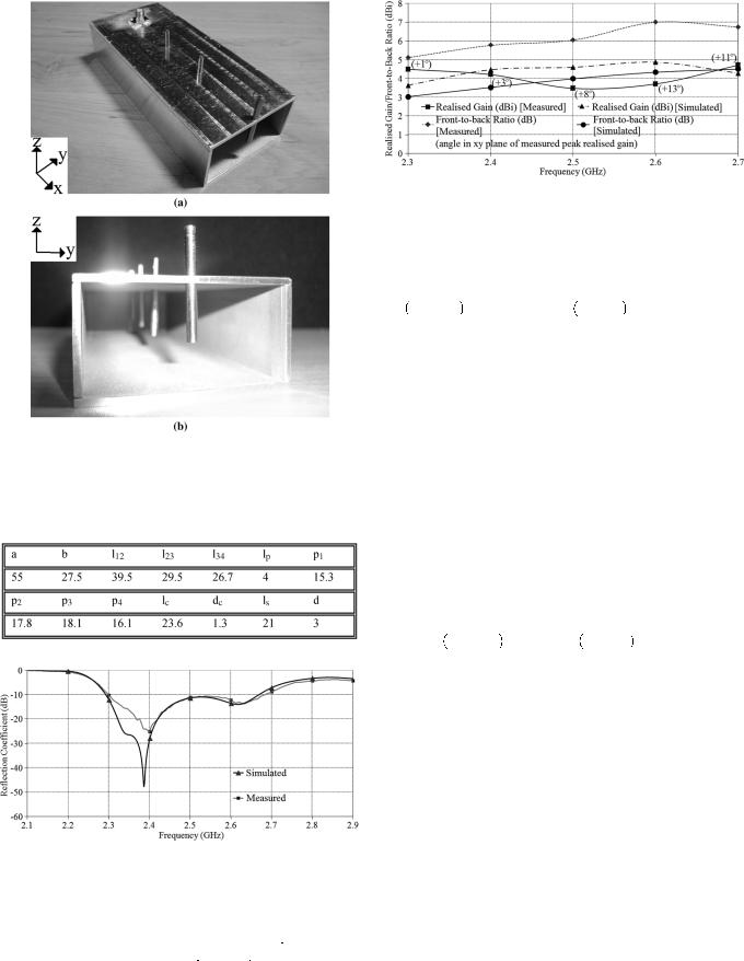
shown in Fig. 7. Aluminium is used to form the waveguide walls |
||||||||||||||||||||||||||||||||||||||||||||||||||||||||||||||||||||||||||||||||||||||||||||||||||||||||||||||||||||||||||||||||||
side of an air-filled waveguide section containing the obstacle, |
while the posts are formed from stainless steel and have been de- |
||||||||||||||||||||||||||||||||||||||||||||||||||||||||||||||||||||||||||||||||||||||||||||||||||||||||||||||||||||||||||||||||||
with waveguide ports used at each side to excite the simulation |
signed such that they may be moved in or out of the waveguide |
||||||||||||||||||||||||||||||||||||||||||||||||||||||||||||||||||||||||||||||||||||||||||||||||||||||||||||||||||||||||||||||||||
in CST. Each port was normalised to a value of characteristic |
for tuning purposes. However it was found that no tuning was |
||||||||||||||||||||||||||||||||||||||||||||||||||||||||||||||||||||||||||||||||||||||||||||||||||||||||||||||||||||||||||||||||||
impedance that, according to the ADS simulation, should give a |
required and so the following results were obtained with pro- |
||||||||||||||||||||||||||||||||||||||||||||||||||||||||||||||||||||||||||||||||||||||||||||||||||||||||||||||||||||||||||||||||||
resonance close to the centre frequency of the antenna (approx- |
trusion of the posts inside the waveguide adjusted to the values |
||||||||||||||||||||||||||||||||||||||||||||||||||||||||||||||||||||||||||||||||||||||||||||||||||||||||||||||||||||||||||||||||||
imately 2.4 GHz) if the shunt capacitance of the post is equal to |
given in Table II. |
|
|
|
|
|
|
|
|
|
|
|
|
|
|
|
|
|
|
|
|
|
|
|
|
|
|
|
|
|
|
|
|
|
|
||||||||||||||||||||||||||||||||||||||||||||||||||||||||||||||||||||||||||||||||||||||||||||||||
that of the ideal shunt capacitance used in ADS; the height of |
|
Fig. 8 shows the measured/simulated variation with fre- |
|||||||||||||||||||||||||||||||||||||||||||||||||||||||||||||||||||||||||||||||||||||||||||||||||||||||||||||||||||||||||||||||||
each post may thus be optimized to give a good match between |
quency of the matching at the input port. The antenna is |
||||||||||||||||||||||||||||||||||||||||||||||||||||||||||||||||||||||||||||||||||||||||||||||||||||||||||||||||||||||||||||||||||
EM and circuit-based simulation results. |
|
|
|
|
|
|
|
|
|
|
|
|
|
|
|
|
|
|
|
|
|
|
|
|
|
|
|
matched over a measured bandwidth of 15.3%, from 2.30–2.68 |
|||||||||||||||||||||||||||||||||||||||||||||||||||||||||||||||||||||||||||||||||||||||||||||||||||||||
|
|
|
The heights of the posts required were found to be: |
|
|
|
|
|
|
|
|
|
|
GHz, for reflection coefficient |
|
|
|
10 dB, i.e. below the domi- |
|||||||||||||||||||||||||||||||||||||||||||||||||||||||||||||||||||||||||||||||||||||||||||||||||||||||||||||||||
|
|
|
|
|
|
|
|
|
|
|
|
|
|
||||||||||||||||||||||||||||||||||||||||||||||||||||||||||||||||||||||||||||||||||||||||||||||||||||||||||||||||||||||
|
|
|
|
|
|
|
|
|
|
|
|
|
|
, |
|
|
|
|
|
|
|
|
|
|
|
|
|
|
|
|
|
, |
|
|
|
|
|
|
|
|
|
|
|
|
|
|
|
|
|
|
|
|
|
|
|
, |
|
|
|
|
|
|
|
|
|
|
|
|
|
|
|
|
. |
nant mode cutoff frequency of the waveguide (which is 2.725 |
|||||||||||||||||||||||||||||||||||||||||||||||||||||||||
|
|
|
|
|
|
|
|
|
|
|
|
|
|
|
|
|
|
|
|
|
|
|
|
|
|
|
|
|
|
||||||||||||||||||||||||||||||||||||||||||||||||||||||||||||||||||||||||||||||||||||||||||||||||||||||
The antenna design was then simulated in CST. To enable this |
GHz). No post tuning was employed. The antenna is matched |
||||||||||||||||||||||||||||||||||||||||||||||||||||||||||||||||||||||||||||||||||||||||||||||||||||||||||||||||||||||||||||||||||
a coaxial probe was designed that matches from the character- |
over a very similar bandwidth to that predicted by simulation |
||||||||||||||||||||||||||||||||||||||||||||||||||||||||||||||||||||||||||||||||||||||||||||||||||||||||||||||||||||||||||||||||||
istic impedance of the coaxial probe, i.e. |
|
|
|
|
|
, to the impedance |
of 14.9% (2.30–2.67 GHz) for reflection coefficient |
|
|
|
10 |
||||||||||||||||||||||||||||||||||||||||||||||||||||||||||||||||||||||||||||||||||||||||||||||||||||||||||||||||||||||||
given by the ratio of electric and magnetic fields at the plane in |
dB. The antenna’s length is |
|
|
|
|
|
|
|
|
and aperture dimensions |
|||||||||||||||||||||||||||||||||||||||||||||||||||||||||||||||||||||||||||||||||||||||||||||||||||||||||||||||||||||||||
|
|
|
|
|
|
|
|
||||||||||||||||||||||||||||||||||||||||||||||||||||||||||||||||||||||||||||||||||||||||||||||||||||||||||||||||||||||||||||
the waveguide a distance |
|
|
|
|
|
|
|
|
|
|
|
|
|
|
|
|
|
|
|
from the first capacitive |
|
|
|
|
|
|
|
|
|
|
|
|
|
|
|
|
|
|
at the highest frequency in the bandwidth |
||||||||||||||||||||||||||||||||||||||||||||||||||||||||||||||||||||||||||||||||||||||||||||
post, i.e. |
|
|
|
|
|
|
|
. The distance |
|
from the back wall to the coaxial |
and it is therefore suitable for use in a wide-angle scanning |
||||||||||||||||||||||||||||||||||||||||||||||||||||||||||||||||||||||||||||||||||||||||||||||||||||||||||||||||||||||||
|
|
|
|
|
|
|
|
|
|||||||||||||||||||||||||||||||||||||||||||||||||||||||||||||||||||||||||||||||||||||||||||||||||||||||||||||||||||||||||||
probe, |
|
|
|
|
|
|
, and the length of the inner conductor of the coaxial |
phased array. The filtering antenna presented in [19] is realised |
|||||||||||||||||||||||||||||||||||||||||||||||||||||||||||||||||||||||||||||||||||||||||||||||||||||||||||||||||||||||||||
|
|
||||||||||||||||||||||||||||||||||||||||||||||||||||||||||||||||||||||||||||||||||||||||||||||||||||||||||||||||||||||||||||||||||
probe, |
|
|
|
|
, were optimized using CST to enable matching over |
in substrate integrated waveguide and therefore is smaller in |
|||||||||||||||||||||||||||||||||||||||||||||||||||||||||||||||||||||||||||||||||||||||||||||||||||||||||||||||||||||||||||||
|
|||||||||||||||||||||||||||||||||||||||||||||||||||||||||||||||||||||||||||||||||||||||||||||||||||||||||||||||||||||||||||||||||||
as wide a bandwidth as possible. Fig. 5 shows that the antenna |
volume, however its area is |
|
|
|
|
|
|
|
|
|
|
|
|
|
|
|
|
|
|
|
at the highest |
||||||||||||||||||||||||||||||||||||||||||||||||||||||||||||||||||||||||||||||||||||||||||||||||||||||||||||||
|
|
|
|
|
|
|
|
|
|
|
|
|
|
||||||||||||||||||||||||||||||||||||||||||||||||||||||||||||||||||||||||||||||||||||||||||||||||||||||||||||||||||||||
has a CST simulated bandwidth of 14.9% (2.3–2.67 GHz) for |
frequency in the bandwidth, larger than that of the presented |
||||||||||||||||||||||||||||||||||||||||||||||||||||||||||||||||||||||||||||||||||||||||||||||||||||||||||||||||||||||||||||||||||
140 |
IEEE TRANSACTIONS ON ANTENNAS AND PROPAGATION, VOL. 61, NO. 1, JANUARY 2013 |
Fig. 7. Fabricated wideband small-aperture evanescent-mode waveguide antenna (a) perspective view (b) front view.
TABLE II
DIMENSIONS OF WIDEBAND SMALL-APERTURE EVANESCENT-MODE
WAVEGUIDE ANTENNA [MM]
Fig. 8. Variation in measured/simulated reflection coefficient of the wideband small-aperture evanescent-mode waveguide antenna with frequency.
design. The filtering antenna presented in [20] is much larger
than the design presented here, approximately |
|
|
|
|
|
|
|
|
in length |
||||||||||||||
|
|
|
|
|
|
||||||||||||||||||
|
|
|
|
|
|
|
|
||||||||||||||||
and with aperture dimensions of |
|
|
|
|
|
|
|
|
|
|
|
|
|
|
|
|
|
at the highest |
|||||
|
|
|
|
|
|
|
|
|
|
|
|
|
|
|
|
|
|||||||
|
|
|
|
|
|
|
|
|
|
|
|
|
|
|
|
|
|
|
|
|
|
|
|
frequency in the bandwidth. The filtering antennas in [19] and [20] are also more narrowband than the presented design, with
a bandwidth of 6.3% for reflection coefficient |
|
|
|
10 dB in |
Fig. 9. Variation in measured/simulated radiation characteristics of the wideband small-aperture evanescent-mode waveguide antenna with frequency.
[19] and a bandwidth of 9% for reflection coefficient |
|
|
|
10 dB |
in [20]. p |
|
|
|
|
The radiation patterns of the antenna were measured in the x-y 


 plane and the x-z


 plane. The variation
in the measured/simulated peak realised gain and front-to-back ratio is shown in Fig. 9. Note that the measured peak realised gain shown in Fig. 9 was recorded in the x-y plane for each frequency point measured, while the peak simulated realised gain occurs at boresight across the bandwidth. Fig. 9 shows that the measured realised gain varies from 3.5–4.73 dBi across the bandwidth, a similar variation to that observed in the simulated results, although the measured realised gain is lower than the simulated value in the centre of the band. Discrepancies between simulated and measured realised gain are of the order of 1 dB and are primarily attributed to fabrication tolerances. The measured front-to-back ratio is higher than the simulated value across the bandwidth, varying from 5.13–7.01 dB. The disparity between simulated and measured results may be due to fabrication tolerances, in particular the joints visible in Fig. 7 between the sides of the waveguide and its top/bottom, which isn’t modelled in the simulations.
The radiation patterns of the antenna are shown in Fig. 10 in the x-y 


 and the x-z


 planes for selected
frequencies in the antenna’s operating band. Note that due to the CST predicted cross-polarisation in the 


 plane being less
than 110 dB, only the measured cross-polarisation is plotted in this plane. It may be observed that measured cross polarisation is fairly low at boresight, with a measured cross-polar ratio  18 dB in the


 plane and
  22 dB in the


 plane
plane
observed across the bandwidth for the patterns shown. Cross polarisation levels are however much higher at the sides and
back of the antenna, particularly in the |
|
|
|
|
|
|
plane. |
V. CONCLUSION
We have presented a design methodology that permits the application of band-pass filter principles to form wideband small-aperture evanescent-mode waveguide antenna designs. A design procedure is outlined that permits matching of antenna aperture admittance of an evanescent-mode open-ended waveguide to a real impedance generator over an approximate bandwidth of 15% or more for reflection coefficient

 10 dB. Capacitive posts and evanescent-mode waveguide sections are used to form the resonators/coupling elements of the antenna. This antenna is fabricated and shows measured

LUDLOW et al.: APPLYING BAND-PASS FILTER TECHNIQUES TO THE DESIGN OF SMALL-APERTURE EVANESCENT-MODE WAVEGUIDE ANTENNAS |
141 |
Fig. 10. Radiation patterns of wideband small-aperture evanescent-mode waveguide antenna measured at (a) 2.3 GHz, 


 plane (b) 2.3 GHz,


 plane
plane
(c) 2.5 GHz, 


 plane (d) 2.5 GHz,


 plane (e) 2.7 GHz,


 plane (f) 2.7 GHz,


 plane.
bandwidth of 15.3%, from 2.30–2.68 GHz, for reflection coefficient 
 10 dB and measured realised gain variation of 3.5–4.73 dBi across the bandwidth. The design has aperture dimensions


 at the highest frequency in the bandwidth. The resulting antenna designs could find utility in a variety of phased array applications, since the design methodology is applicable for any waveguide dimensions.
ACKNOWLEDGMENT
The authors would like to thank M. Major, J. Knox, and J. Megarry for the construction of the antenna elements used in this work and the author of [10] for providing them with his report.
REFERENCES
[1]H. A. Wheeler, “The radiation resistance of an antenna in an infinite array or waveguide,” Proc. IRE, vol. 36, no. 4, pp. 478–487, Apr. 1948.
[2]L. Stark, “Microwave theory of phased array antennas—A review,” Proc. IEEE, vol. 62, no. 12, pp. 1661–1701, Dec. 1974.
[3]R. J. Mailloux, “Phased array theory and technology,” Proc. IEEE, vol. 70, no. 3, pp. 246–291, Mar. 1982.
[4]L. Lewin, Advanced Theory of Waveguides. London, England: Iliffe, 1951.
[5]D. P. Tran, M. Tian, and L. P. Ligthart, “Theory and practice of a novel miniature radiator: The microstrip-like antenna,” presented at the Mediterranean Electrotechnical Conference, Antalya, Turkey, 1994.
[6]M. Hajian, D. P. Tran, and L. P. Ligthart, “Design of a wideband miniature dielectric-filled waveguide antenna for collision avoidance radar,” IEEE Antennas Propag. Mag., vol. 42, no. 1, pp. 34–40, Feb. 2000.
[7]M. N. M. Kehn and P. S. Kildal, “Miniaturized rectangular hard waveguides for use in multifrequency phased arrays,” IEEE Trans. Antennas Propag., vol. 53, no. 1, pp. 100–109, Jan. 2005.
[8]R. Chernobrovkin, I. Ivanchenko, A. Korolev, and L. P. Ligthart et al., “Wide-band antenna array,” presented at the Eur. Microwave Conf., Amsterdam, Netherlands, Oct. 2008.
[9]S. Hrabar, “Miniaturized open-ended radiator based on waveguide filled with uniaxial negative permeability metamaterial,” presented at the IEEE Antennas Propag. Society Int. Symp., Washington D.C., Jul. 2005.
[10]A. R. Lopez, Wideband Dual-polarised Element For a Phased Array Antenna Wheeler Laboratory, Hazeltine Corporation, Greenlawn, New York, Tech. Rep. No. AFAL-TR-74-000, Jun. 1974.
[11]S. J. Foti and M. W. Shelley, “An experimental wideband polarisation diverse phased array,” in Proc. Military Microwaves, Jul. 1990, no. 7, pp. 263–271.
[12]P. Ludlow and V. Fusco, “Matching evanescent open-ended waveguide antennas using the Imaginary Smith Chart,” presented at the Eur. Conf. Antennas Propag., Rome, Italy, Apr. 2011.

142 |
IEEE TRANSACTIONS ON ANTENNAS AND PROPAGATION, VOL. 61, NO. 1, JANUARY 2013 |
[13]P. Ludlow and V. Fusco, “Reconfigurable small-aperture evanescent waveguide antenna,” IEEE Trans. Antennas Propag., vol. 59, no. 12, pp. 4815–4819, Dec. 2011.
[14]G. F. Craven and C. K. Mok, “The design of evanescent mode waveguide bandpass filters for a prescribed insertion loss characteristic,”
IEEE Trans. Microwave Theory Tech., vol. 19, no. 3, Mar. 1971.
[15]Advanced Design System (ADS), 2008 [Online]. Available: www.ag- ilent.com/find/eesof-ads
[16]Computer Simulation Technology (CST), Microwave Studio, 2010 [Online]. Available: www.cst.com
[17]G. L. Matthaei, L. Young, and E. M. T. Jones, Microwave Filters, Impedance-Matching Networks and Coupling Structures. North Bergen, NJ: Artech House, 1980.
[18]G. F. Craven and R. F. Skedd, Evanescent Mode Microwave Components. Boston, MA: Artech House, 1987.
[19]Y. Yusuf and X. Gong, “Compact low-loss integration of high-Q 3-D filters with highly efficient antennas,” IEEE Trans. Microwave Theory Tech., vol. 59, no. 4, Apr. 2011.
[20]Y. Yang and M. Lancaster, “Waveguide slot antenna with integrated filters,” presented at the ESA Workshop on Antennas for Space Applications, Noordwijk, Netherlands, Oct. 2010, pp. 48–54.
[21]A. R. Lopez, “Review of narrowband impedance-matching limitations,” IEEE Antennas Propag. Mag., vol. 46, no. 4, pp. 88–90, Aug. 2004.
[22]R. V. Lowman and R. N. Simons, “Transmission lines and waveguides,” in Antenna Engineering Handbook, J. L. Volakis, Ed., 4th ed. New York: McGraw-Hill, 2007.
Peter Ludlow received the M.Eng. degree in electrical and electronic engineering and the Ph.D. degree in microwave electronics from Queen’s University Belfast (QUB), Belfast, Northern Ireland, in 2008 and 2011, respectively.
He joined Lamhroe, a spin-off company from Queen’s University Belfast, as an Engineer in 2011, and is currently employed by them, working on the design of a microwave perimeter intrusion detection system.
Dr. Ludlow was nominated for the Best Student Paper Award at the 5th European Conference on Antennas and Propagation (EUCAP), held in Rome, Italy in April 2011.
Vincent Fusco (S’82–M’82–SM’96–F’04) received the Bachelor’s degree (1st class honors) in electrical and electronic engineering, the Ph.D. degree in microwave electronics, and the D.Sc. degree, for his work on advanced front end architectures with enhanced functionality, from The Queens University of Belfast (QUB), Belfast, Northern Ireland, in 1979, 1982, and 2000, respectively.
He is the Technical Director of the High Frequency Laboratories, Queens University of Belfast, and is also Director of the International Centre
for Research for System on Chip and Advanced MicroWireless Integration, SoCaM. His research interests include nonlinear microwave circuit design, and active and passive antenna techniques. He has published over 420 scientific papers in major journals and international conferences, and is the author of two textbooks. He holds several patents on active and retrodirective antennas and has contributed invited chapters to books in the fields of active antenna design and EM field computation.
Prof. Fusco is a Fellow of the Royal Academy of Engineering and a Fellow of the Institution of Electrical Engineers (U.K.). In 1986, he was awarded a British Telecommunications Fellowship and 1997 he was awarded the NI Engineering Federation Trophy for outstanding industrially relevant research.
George Goussetis (S’99–M’02–SM’12) received the Diploma degree in Electrical and Computer Engineering from the National Technical University of Athens, Greece, in 1998, and the Ph.D. degree from the University of Westminster, London, UK, in 2002. In 2002 he also graduated B.Sc. in physics (first class) from University College London (UCL), UK.
In 1998, he joined the Space Engineering, Rome, Italy, as RF Engineer and in 1999 the Wireless Communications Research Group, University of
Westminster, UK, as a Research Assistant. Between 2002 and 2006 he was a Senior Research Fellow at Loughborough University, UK. Between 2006 and 2009 he was a Lecturer (Assistant Professor) with the School of Engineering and Physical Sciences, Heriot-Watt University, Edinburgh, UK. He joined the Institute of Electronics Communications and Information Technology at Queen’s University Belfast, UK, in September 2009 as a Reader (Associate Professor). He has authored or coauthored over 150 peer-reviewed papers three book chapters and two patents. His research interests include the modelling and design of microwave filters, frequency-selective surfaces and periodic structures, leaky wave antennas, microwave sensing and curing as well numerical techniques for electromagnetics.
Dr. Goussetis has held a research fellowship from the Onassis foundation in 2001, a research fellowship from the UK Royal Academy of Engineering between 2006-2011 and a European Marie-Curie experienced researcher fellowship in 2011. In 2010 he was visiting Professor in UPCT, Spain. He is the co-recipient of the 2011 European Space Agency young engineer of the year prize, the 2011 EuCAP best student paper prize and the 2012 EuCAP best antenna theory paper prize.
Dmitry E. Zelenchuk (S’02–M’05) received the B.Sc. and M.Sc. degrees in Physics and the Ph.D. degree in Radiophysics from Rostov State University (Russia) in 1999, 2001 and 2004, respectively.
From 2003 to 2005 he was a Lecturer at the Dept. of Applied Electrodynamics and Computer Modelling, Rostov State University, Russia. Currently he is a Research Fellow at Queen’s University Belfast, UK. His research interests include numerical and analytical methods for the problems of electromagnetic field theory, material characterization; mm-wave cir-
cuits, antennas and advanced packaging; imaging; phase conjugating and timereversal phenomena in complex environments; frequency selective surfaces, linear and nonlinear phenomena in planar circuits and antennas, including passive intermodulation, and various physical phenomena of plasmonic and nanostructures. He has published more than 60 journal and conference papers and a book chapter and has also been a session chair at scientific conferences.
In 2001 Dr. Zelenchuk was awarded the medal of Ministry of Education of the Russian Federation “For the Best Scientific Student Paper” for the paper “Conductor Loss in Superconducting Slot Line”.