

Sådhanå |
(2021) 46:74 |
Page 5 of 8 |
74 |
Figure 10. Response of the proposed DRA (a) S11 and Efficiency, (b) Gain.
multiple TZs as mentioned in [27]. Equivalent circuit representation of the coupled configuration is shown in figure 3, where Lm arise due to magnetic coupling and the electric coupling between the resonators gives rise to the capacitors Ce1 and Ce2. By carefully adjusting the equivalent coupling parameters (Lm=1.5 nH, Ce1=0.04 pF and Ce2=0.01 pF), four transmission zeros can be allocated at desired positions.
3. Results and verification
3.1 Analysis of multiple radiation nulls
A comparative study is demonstrated here between conventional slot-coupled DRA (Conv. DRA) and the proposed high-selective filtering DRA. S11-plots are presented in figure 4 (a) and it is evident from figure that Conv. DRA resonates at 3.27 GHz. On the other hand, different loading effect caused by the HSFN leads to resonate the proposed filtering DRA at three distinctive resonant frequencies in close proximity. S11 of the proposed design touches nearly
Figure 11. Simulated and Measured radiation pattern of the proposed DRA at (a) 3.14 GHz, (b) 3.3 GHz and (c) 3.48 GHz.
0 dB beyond pass-band which ensures skirt filtering performance. The gain response demonstrated in figure 4(b) further substantiates the filtering nature of the proposed antenna. No sharp dropping in gain is observed outside the operating band for the Conv. DRA. Whereas, the introduction of the HSFN inevitably surges the frequency selectivity of the DRA. A sharp transition in the gain response of antenna ahead of the passband is easily discernable with four radiation nulls at RN1 = 2.52 GHz, RN2=2.78 GHz, RN3=3.70 GHz and RN4 = 4.0 GHz. The two nulls i.e. RN1, RN2 at lower band-edge occur due to the presence of transmission zero generated by band-rejection resonator pair (R1p) whereas the other two nulls i.e. RN3, RN4 at upper band-edge occur due to the presence of transmission zero generated by band-rejection resonator pair (R2p). Negligible amount of energy transferred to the DRA from feed line at those frequencies, produces the nulls in the gain response [17].
Radiation Nulls of the DRA can be positioned at suitable locations as per requirement just by varying the length of band reject resonator pairs (R1p and R2p). From figure 5(a), it is clear that the frequency selectivity at lower band edge can be adjusted by varying the length of R1p. As lr1 changes from 20.4 mm to 19.1 mm, nulls at lower band

74 |
Page 6 of 8 |
|
|
|
|
|
|
|
|
|
|
||||
|
This Work |
|
Rectangular |
Band-rejection |
Resonator Pair |
3.31 GHz |
11.8 % |
0.4790.44 |
5.6 dBi |
4 |
Varying length of |
band-reject resonator |
LBE:2.52-2.98 GHz |
UBE:3.48-4.18 GHz |
|
|
|
|
|||||||||||||
|
2019],21[ |
|
Cylindrical |
StubsMicrostrip |
lengthdifferentof |
GHz2.4 |
7% |
k(dia=0.204Circular |
dBi3.05 |
2 |
N.A |
|
N.A |
|
|
|
|
|
|
|
|
|
|
) |
|
|
|
|
|
|
|
|
|
|
|
|
|
|
|
0 |
|
|
|
|
|
|
|
|
[22], 2018 |
|
Rectangular |
Semi-elliptical |
shaped bandpass filter |
8.15 GHz |
6.13% |
1.00590.95 |
5.33 dBic |
2 |
N.A |
|
N.A |
|
|
|
],24[ 2019 |
|
withRectangularslots |
CoatedSilverSlots and |
mode |
ExtremlyGHz4.17 Narrow |
\100( MHz) |
0.6190.65 |
dBi4.8 |
2 |
theVarying |
silvercoated slots |
IndividualNo |
Controlling |
|
|
|
|
|||||||||||||
|
|
radiating-NonTM |
|
||||||||||||
|
|
|
|
|
111 |
|
|
|
|
|
|
|
|
|
|
of the DRA with Filtering Characteristics. |
[17], 2016 [19], 2018 |
|
Complex Rectangular |
Parallel Strips Hybrid feed Using |
con-formal strip |
4.92 GHz 1.965 GHz |
20.3 % 21.9 % |
1.2390.82 0.4490.44 |
9.05 dBi 5.1 dBi |
2 2 |
Different Changing |
length of parallel strips length of |
microstrip stubs N.A LBE:1.5 -1.6 GHz |
UBE:2.2-2.33 GHz |
LBE lower band-edge, UBE upper band-edge. |
1.TablePerformances |
Year[Ref], |
|
ShapeDRA |
FilteringofMathod |
|
frequencyCentre |
(f |
kx |
GainAvg. |
RNsofNo. |
Controlling |
RNsofScheme |
Controling |
RNsofRange |
k |
|
|
|
|
|
|
|
Bandwidth), |
0 |
|
|
|
|
|
|
wavelength,freespace |
|
|
|
|
|
|
|
|
0 |
|
|
|
|
|
|
|
|
|
|
|
|
|
|
|
yk |
|
|
|
|
|
|
|
|
|
|
|
|
|
|
0 |
|
|
|
|
|
|
|
0 |
|
|
|
|
|
|
|
|
|
|
|
|
|
|
|
|
Sådhanå |
(2021) 46:74 |
edge varies from 2.52 GHz to 2.98 GHz but selectivity at upper band edge remain intact. Figure 5(b) shows the gain response for different lengths of lr2 (14.6 mm to 13.1 mm). Both the radiations nulls at upper band edge shift positions from 3.48 GHz to 4.18GHz but no changes are observed in lower band edge. The launching of TE111 mode within the rectangular DRA is confirmed for all three frequencies within the passband from the simulated E-fields as depicted in figure 6, which ensure broadside radiation throughout the passband. The high -selective filtering network (HSFN) has two transmission poles which is integrated with the DRA, produced different loading effect on the resonant mode of the DRA in the passband and the fundamental mode frequency is split and slightly deviated from each other. Hence the composite system produced a triple pole response.
3.2 Higher Order Mode Elimination
As the aspect ratio of RDRA governs the resonant frequency of different modes, the conventional DRA also resonates at higher-order mode at nearly 4.5 GHz, as shown in figure 4(a). The electric field distribution plot in figure 7(a) verify that the conventional DRA resonates in higher-order mode at 4.5 GHz. But the integration of high selective filtering network (HSFN) eliminates the higherorder mode, as it resides outside the passband of the HFSN. The electric field distribution plot in figure 7(b) verifies that almost no energy is coupled to the DRA at 4.5 GHz when HSFN is integrated with the DRA’s feedline. Surface current distribution in the feedline of the proposed DRA at 4.5 GHz is plotted in figure 8. As shown in the figure, current mainly concentrates in high -selective filtering network (HSFN), a negligible amount of energy can be coupled to the DRA through the coupling slot at 4.5 GHz.
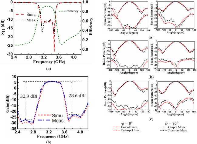
3.3 Measurement verification
The feed network is constructed on Arlon AD270 laminate and the DRA is implemented from ECCOSTOCK Hik ceramic as displayed in figure 9. Little amount of adhesive is used to attach the DRA with the substrate. A vector network analyser manufactured by Agilent with model no: N5230A is used to perform the S-parameter measurement. Measured result coincides with simulation result. The antenna operates from 3.12 GHz to 3.51 GHz (bandwidth=11.8%) as shown in figure 10(a). A consistent broadside gain in passband with a peak value 5.81 dBi is achieved from fabricated prototype as depicted in figure 10(b). The sharp plunge in gain below -28.5 dBi, -29.2 dBi, -26.6 dBi and -24.6 dBi at 2.5 GHz, 2.8 GHz, 3.7 GHz and 4.0 GHz respectively, experimentally validate the existence of four radiation nulls in gain vs frequency response of the proposed design. Out of band suppression of lower than 28 dB from peak value is achieved in