

J Comput Electron
0 |
|
|
|
|
|
|
|
|
|
|
|
|
|
|
|
|
S11 [dB] |
εr=2.55 |
|
−5 |
|
|
|
|
|
|
εr=2.55 |
||
|
|
|
|
|
|
|
|
εr=2.59 |
|
|
|
|
|
|
|
|
|
|
|
|
|
|
|
|
|
|
|
|
εr=2.59 |
−10 |
|
|
|
|
|
|
|
|
εr=2.51 |
|
|
S21 [dB] |
|
|
|
|
|
|
εr=2.51 |
|
|
|
|
|
|
|
|
|
|
−15 |
|
|
|
|
|
|
|
|
|
−20 |
|
|
|
|
|
|
|
|
|
10 |
10.25 |
10.5 |
10.75 |
11 |
11.25 |
11.5 |
11.75 |
12 |
|
|
|
|
|
f [GHz] |
|
|
|
|
|
|
|
|
|
(a) |
|
|
|
|
|
0 |
|
|
|
|
|
|
|
εr= 2.55 |
|
|
|
|
|
|
S |
|
[dB] |
||
−10 |
|
|
|
|
11 |
|
εr= 2.55 |
||
|
|
|
|
|
|
|
|||
|
|
|
|
|
|
|
|
||
−20 |
|
|
|
|
|
|
|
εr= 2.59 |
|
−30 |
|
|
|
|
|
|
|
εr= 2.59 |
|
|
|
|
|
|
|
|
εr = 2.51 |
||
|
|
|
|
|
|
|
|
||
−40 |
|
|
|
|
|
|
|
εr = 2.51 |
|
−50 |
|
S21 [dB] |
|
|
|
|
|
|
|
−60 |
|
|
|
|
|
|
|
|
|
10 |
10.25 |
10.5 |
10.75 |
11 |
11.25 |
|
11.5 |
11.75 |
12 |
|
|
|
|
f [GHz] |
|
|
|
|
|
(b)
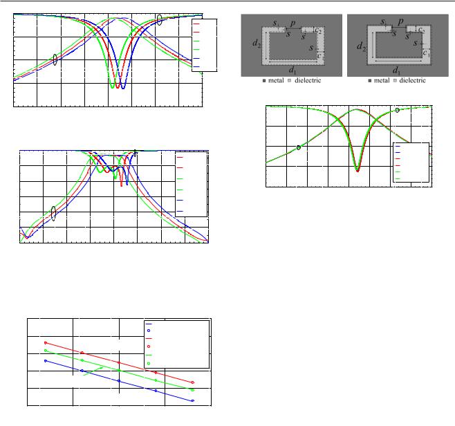
Fig. 3 Comparison of amplitude responses for various values of r : a waveguide resonator, b waveguide Þlter (Color Þgure online)
|
11.3 |
|
|
Filter − Sim |
|
||
|
|
|
|
|
|||
|
11.2 |
|
|
Filter − Approx |
|
||
|
|
fr=−1.43εr+14.694 |
1st/3rd resonator − Sim |
|
|||
|
|
|
1st/3rd resonator − Approx |
||||
[GHz] |
11.1 |
|
|
2 |
nd |
resonator − Sim |
|
|
|
|
|
|
|||
11 |
|
|
2nd resonator − Approx |
|
|||
r |
|
|
|
|
|
|
|
f |
|
|
|
|
|
|
|
|
|
|
|
|
|
|
|
|
10.9 |
fr=−1.43εr+14.650 |
|
|
|
|
|
|
|
|
|
|
|
|
|
|
10.8 |
|
fr=−1.43εr+14.590 |
|
|
||
|
|
|
|
|
|
|
|
|
2.45 |
2.5 |
2.55 |
|
|
2.6 |
2.65 |
|
|
|
εr |
|
|
|
|
Fig. 4 Change of resonant frequency with permittivity, with the best linear Þt to each experimental dataset (Color Þgure online)
this measurement and the proposed design curve the exact permittivity determined.
3.2Imperfections and inaccuracy of the machine used for fabrication
The tolerance of the machine used for fabrication may also have a relevant impact on the frequency response; namely, the inaccuracy introduced by the machine during the process of printed-circuit board fabrication may affect the waveguide resonator and Þlter response. Herein, we consider some of the possible issues related to machine tolerance.
|
(a) |
|
|
|
(b) |
|
||
0 |
|
|
|
|
|
|
|
|
|
|
|
|
|
|
|
S11 [dB] |
|
−5 |
|
|
|
|
|
|
|
|
−10 |
|
|
|
|
|
|
original |
|
|
|
S21 [dB] |
|
|
|
|
original |
|
|
|
|
|
|
|
increased |
|
|
−15 |
|
|
|
|
|
|
increased |
|
|
|
|
|
|
|
|
decreased |
|
|
|
|
|
|
|
|
decreased |
|
−20 |
|
|
|
|
|
|
|
|
10 |
10.25 |
10.5 |
10.75 |
11 |
11.25 |
11.5 |
11.75 |
12 |
f [GHz]
(c)
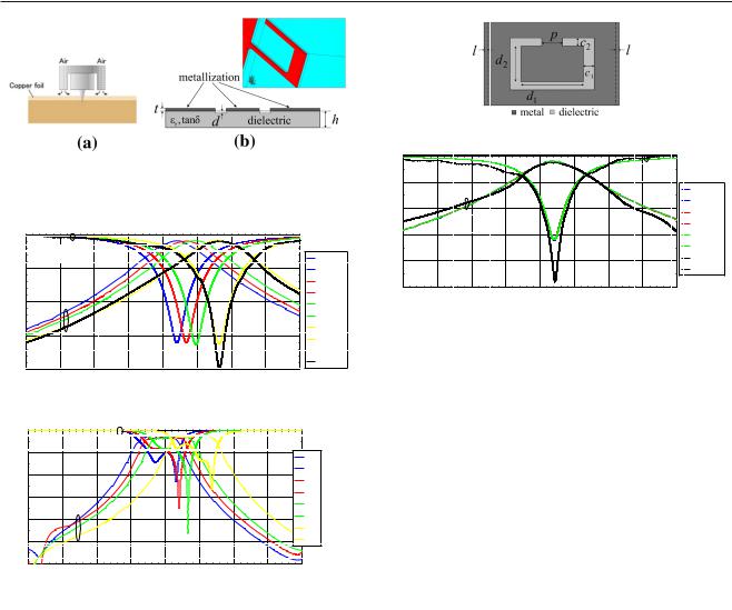
Fig. 5 Changes of resonator dimensions: a dimensions decreased by s, b dimensions increased by s, c comparison of amplitude responses for the waveguide resonator (Color Þgure online)
When using a milling process for fabrication, one may obtain CSRRs with larger or smaller dimensions than the desired design value, as a consequence of inaccuracy during its operation, as depicted in Fig. 5a, b. For the considered model, it is assumed that s = 2.5 µm, meaning that the width of the resonator trace is increased or decreased by 5 µm in total. A comparison of the amplitude responses is shown in Fig. 5c, revealing no signiÞcant change in the waveguide resonator response. Practically, there is no change of the waveguide Þlter response either, when the dimensions of the CSRRs are modiÞed as described above. The accuracy of the traces certainly depends on the accuracy of the machine used for fabrication; however, if the deviation of the desired trace width is within the aforementioned limits (±5 µm), there is no degradation of the amplitude response.
When the milling process is used to remove the metallization, the tool may dig into the substrate to a certain depth, as elaborated in [29]. However, the machine uses a noncontact board-making system, meaning there is no undesirable trace on the board surface (copper foil) (Fig. 6a). Herein, a cylindrical tool was used to model this effect. The cross-section of the printed-circuit board is depicted in Fig. 6b, along with the detail of the WIPL-D model of the insert. For the third-order Þlter, the same value of the depth d is assumed for each printed-circuit insert. The amplitude responses for various values of the depth d are compared in Fig. 7. With increasing depth, the center frequency moves toward higher values, and the bandwidth becomes wider, for both the waveguide resonator and Þlter. The digging depth of 10 µm can be declared as critical for a single insert, since higher values cause sig-
123
J Comput Electron
Fig. 6 a Noncontact board-making system (http://www.mitspcb. com/), b proÞle of the printed-circuit board when the tool digs into the substrate, and WIPL-D model
0 |
|
|
d [μm] |
|
|
S11 [dB] |
|||
−5 |
0 |
|||
|
|
0 |
||
|
|
|
10 |
|
−10 |
|
|
10 |
|
|
|
20 |
||
|
|
|
20 |
|
−15 |
|
|
50 |
|
S21 |
[dB] |
50 |
||
|
||||
|
|
|
50:Exp |
|
|
|
|
50:Exp |
|
−20 |
|
|
|
|
|
|
|
|
10 |
10.25 |
10.5 |
10.75 |
11 |
11.25 |
11.5 |
11.75 |
12 |
|
|
|
|
f [GHz] |
|
|
|
|
|
|
|
|
(a) |
|
|
|
|
0 |
S11 [GHz] |
|
|
|
|
|
|
|
−10 |
|
|
|
|
|
d [μm] |
||
|
|
|
|
|
|
|
0 |
|
|
|
|
|
|
|
|
|
|
−20 |
|
|
|
|
|
|
|
0 |
|
|
|
|
|
|
|
10 |
|
|
|
|
|
|
|
|
|
|
−30 |
|
|
|
|
|
|
|
10 |
|
|
|
|
|
|
|
20 |
|
|
|
|
|
|
|
|
|
|
−40 |
|
|
|
|
|
|
|
20 |
|
|
|
|
|
|
|
50 |
|
|
|
|
|
|
|
|
|
|
−50 |
S21 [GHz] |
|
|
|
|
|
50 |
|
−60 |
|
|
|
|
|
|
||
|
|
|
|
|
|
|
|
|
10 |
10.25 |
10.5 |
10.75 |
11 |
11.25 |
11.5 |
11.75 |
12 |
|
|
|
|
f [GHz] |
|
|
|
|
|
|
|
|
(b) |
|
|
|
|
Fig. 7 Comparison of amplitude responses for various values of digging depth d for: a waveguide resonator, with comparison of simulation and measurement for d = 50 µm, and b waveguide Þlter (Color Þgure online)
niÞcant amplitude response degradation, primarily in terms of the desired center frequency and bandwidth. For the Þlter using three inserts with the same digging depth, the value should even be lower than 10 µm (around 50 % of the metallization thickness), if possible. The good match between the simulation and measurement results for the amplitude response of the waveguide resonator (Fig. 7a), for the digging depth d = 50 µm, conÞrms the correctness of the applied method for modeling the inßuence of the considered effect in software.
The other possible issue related to the fabrication process is that the printed-circuit inserts may have dimensions that are not exactly the same as those of the waveguide crosssection. Here, we consider plates narrowed by the same amount on both sides, as depicted in Fig. 8a. The comparison of the amplitude responses in Fig. 8b shows that
|
|
|
|
(a) |
|
|
|
|
0 |
|
|
|
|
|
|
|
|
−5 |
|
|
|
|
|
|
S11 [dB] |
l [μm] |
|
|
|
|
|
|
|
0 |
|
|
|
|
|
|
|
|
|
|
−10 |
|
|
|
|
|
|
|
0 |
|
|
|
|
|
|
|
200 |
|
|
|
S21 [dB] |
|
|
|
|
|
|
−15 |
|
|
|
|
|
|
200 |
|
|
|
|
|
|
|
|
500 |
|
|
|
|
|
|
|
|
|
500 |
−20 |
|
|
|
|
|
|
|
500:Exp |
|
|
|
|
|
|
|
500:Exp |
|
|
|
|
|
|
|
|
|
|
−25 |
|
|
|
|
|
|
|
|
10 |
10.25 |
10.5 |
10.75 |
11 |
11.25 |
11.5 |
11.75 |
12 |
|
|
|
|
f [GHz] |
|
|
|
|
(b)
Fig. 8 a Printed-circuit insert narrowed by the same amount l on both sides, b comparison of amplitude responses for various values of l, and comparison of simulation and measurement results for the waveguide resonator for the case l = 500 µm (Color Þgure online)
the center frequency and bandwidth remained unchanged when one dimension of the insert did not exactly match the corresponding dimension of the waveguide. The amplitude response was experimentally veriÞed for the case of a printedcircuit board narrowed by the same amount l = 500 µm on both sides, corresponding to half the width of the tool used for cutting out the plate. This result is also shown in Fig. 8b. Based on the good agreement between the obtained amplitude responses, one can conclude that the model correctly represents the considered effect. Also, it is conÞrmed that this effect practically does not inßuence the amplitude response, in spite of the fact that the insert is not physically short-circuited to all the waveguide walls. For the third-order Þlter, we assumed that each insert was fabricated in the same way, with each being narrowed by the same amount on both sides. Similarly as for the waveguide resonator, the amplitude response was not degraded when one dimension of the insert did not exactly match the corresponding dimension of the waveguide cross-section. These results conÞrm the assumption regarding device robustness in terms of fabrication. For the considered case of inserts narrowed by the same amount on both sides, it is recommended to keep this amount below l = 500 µm (i.e., 1000 µm in total), in order to avoid Þlter response degradation.
3.3 Precise positioning of printed-circuit inserts
During the measurement procedure, it is important that the inserts are stably and precisely positioned in the rectangular waveguide. However, it is not always possible to achieve this,
123
J Comput Electron
(a)
|
|
|
|
(b) |
|
|
|
|
0 |
|
|
|
|
|
|
|
|
|
S11 [dB] |
|
|
|
|
|
|
|
−5 |
|
|
|
|
|
|
|
|
−10 |
|
|
|
|
|
|
original |
|
|
|
|
|
|
|
|
|
|
|
|
|
|
|
|
|
original |
|
−15 |
S21 [dB] |
|
|
|
|
|
inclined |
|
|
|
|
|
|
|
inclined |
|
|
|
|
|
|
|
|
|
rotated |
|
−20 |
|
|
|
|
|
|
rotated |
|
|
|
|
|
|
|
|
|
|
10 |
10.25 |
10.5 |
10.75 |
11 |
11.25 |
11.5 |
11.75 |
12 |
f [GHz]
(c)
Fig. 9 Printed-circuit insert a inclined by α (side view), with WIPL-D model, and b rotated by θ (top view), with WIPL-D model; c comparison of amplitude responses when the insert is inclined or rotated (Color Þgure online)
so it is useful to investigate the effects of inaccuracy related to the position of the inserts on the resonator and Þlter response.
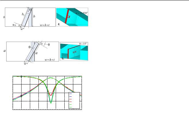
For the waveguide resonator, we consider two possible issues. In the Þrst example, the amplitude response of the resonator with an inclined insert is investigated (Fig. 9a). When the dimensions of the fabricated insert perfectly match the dimensions of the waveguide cross-section (b1 = b), the inclination angle can be calculated according to the following equation:
cos(α) = |
b |
x = |
2bw2 |
(3) |
||
|
, |
|
. |
|||
b + x |
b2 − w2 |
|||||
The critical inclination angle for this case (α ≈ 13◦) still allows the insert to remain in contact with the top and bottom waveguide walls, so it can remain more or less stable inside the waveguide. On the other hand, if the insert is not fabricated accurately enough, being shorter than expected (b1 = b), the inclination angle which still allows this shorter insert to remain stable in the waveguide, for known value of its new height b1, can be found from the following equation:
cos(α) |
|
|
b |
, x |
= |
|
b1w2 wb |
w2 + b12 − b2 |
. (4) |
|
= b1 |
+ x |
b2 − w2 |
||||||||
|
|
|
|
|||||||
For the shorter insert, the inclination angle α can take lower values (e.g., α = 4◦) compared with the case when b1 = b. The other possible issue is that the insert may be slightly rotated, as shown in Fig. 9b. The minimum rotation angle for the considered insert can be calculated according to the following equation:
cos(θ ) = |
a/2 |
x = |
aw2 |
(5) |
||
|
, |
|
. |
|||
a/2 + x |
a2 − w2 |
|||||
For an insert whose dimensions perfectly match the waveguide cross-section, the minimum angle is around 6◦. We consider a waveguide resonator with the insert rotated by θ = 15◦ (positively or negatively), which is the maximum rotation angle that does not cause response degradation. In this case, the insert should remain stable, since it has physical contact with the waveguide walls over the entire surface of its top and bottom side, although it is not short-circuited to the side walls.
According to the obtained results (Fig. 9c), for both considered positions of the insert, there is no signiÞcant inßuence on the resonator amplitude response, hence this type of inaccuracy does not introduce signiÞcant error during the measurement procedure. Also, if such a change in position occurs during regular operation, signiÞcant degradation of the resonator response is not expected.
Regarding the third-order Þlter, precise positioning of the inserts is also a signiÞcant aspect of this research, since it is important to preserve the required lengths of the inverters between the resonators. For waveguide Þlters, inverters are implemented as quarter-wave sections of the waveguide, as mentioned above. Thus, when changing the position of a single insert, the length of the inverter is changed and the Þlter operation may be jeopardized. In this work, we investigated in detail the Þlter response when one or multiple inserts were rotated or inclined.
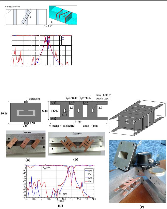
In the case of rotation of a single insert, the obtained results show that the maximum rotation angle for which the amplitude response is preserved and meets the aforementioned conditions is θ = 15◦. We chose to rotate the central insert by θ = 15◦ (Fig. 10a), while the positions of the other two inserts remained unchanged. This was modeled in WIPL-D software, as shown in Fig. 10b. According to the obtained results (Fig. 10c), there was no signiÞcant inßuence on the Þlter response in the passband, hence this type of inaccuracy does not introduce signiÞcant error during the measurement procedure. Also, if such a change of position occurs during regular operation, signiÞcant degradation of the Þlter response is not expected, for the considered or smaller rotation angles.
These results were also veriÞed experimentally by rotating the central insert by the mentioned angle. To enable precise positioning of the inserts, a ladder-like Þxture was
123
J Comput Electron
|
|
(a) |
|
|
|
|
|
|
(b) |
|
|
|
|
|
|
|
|
|
|
|
|
0 |
|
|
|
S11 |
[dB] |
|
|
|
Original |
|
|
|
|
|
|
|
|
||||
−10 |
|
|
|
|
|
|
Original |
|||
|
|
|
|
|
|
|
|
Rotated |
||
|
|
|
|
|
|
|
|
|
||
−20 |
|
|
|
|
|
|
|
|
Rotated |
|
|
|
|
|
|
|
|
|
|
|
|
−30 |
|
|
|
|
|
|
|
|
|
|
−40 |
|
|
|
S21 [dB] |
|
|
|
|
|
|
|
|
|
|
|
|
|
|
|
|
|
−50 |
|
|
|
|
|
|
|
|
|
|
−608 |
8.5 |
9 |
9.5 |
10 |
10.5 |
11 |
11.5 |
12 |
12.5 |
13 |
|
|
|
|
|
f [GHz] |
|
|
|
|
|
|
|
|
|
|
(c) |
|
|
|
|
|
Fig. 10 a Central printed-circuit insert rotated by θ = 15◦ (top view), b WIPL-D model, and c comparison of amplitude responses (Color Þgure online)
designed [30] to hold the inserts, including the rotated one (Fig. 11). Small holes were made at appropriate positions so that the distance between the inserts corresponded to the waveguide section representing the inverter (λg/4 for the observed center frequency). On the other hand, the inserts were modiÞed so they could be attached to the ladder structure (their height was reduced and extensions were added). The dimensions of the holes in the Þxture and the extensions on the inserts were matched, so that the extensions could be easily placed in the holes to Þx them. The inserts and ladder structure are shown in Fig. 11a, b. The fabricated printed-circuit inserts, along with the supporting structure, were placed inside the waveguide used for the measurement, as shown in Fig. 11c. A comparison of the simulated and measured amplitude responses for this case is presented in Fig. 11d, conÞrming the statement above regarding the preserved amplitude response in the passband, compared with the original Þlter.
Besides this example with a single rotated insert, we also investigated the cases with two or three rotated inserts, since
Fig. 11 a Printed-circuit inserts, b ladder structure used for precise positioning, c fabricated printed-circuit inserts, along with the supporting structure, placed inside the waveguide used for measurement, d
comparison of simulated and measured amplitude responses when the central insert is rotated by θ = 15◦ (Color Þgure online)
123