

J Comput Electron
2 Waveguide SRR
Design of the SRR is the Þrst step in the bandstop waveguide Þlter design. For the SRR and Þlter design, WR-90 rectangular waveguide of width a = 22.86 mm and height b = 10.16 mm is used. Inside the waveguide, the dominant mode of propagation is the transverse electric TE10 mode. The printed-circuit inserts are implemented using a copper clad PTFE/woven glass laminate (TLT-6) from Taconic (www.taconic-add.com), with the dielectric permittivity εr = 2.65 ± 0.05, tanδ = 0.0019, substrate thickness h = 1.143 mm and metallization thickness t = 0.018 mm. In order for the losses due to the skin effect and surface roughness to be taken into account, the conductivity was set to σ = 20 MS/m.
2.1 Design algorithm for the waveguide SRR
This subsection reviews an efÞcient sequence of steps for the design of the waveguide SRR. Results of the extensive investigations of the effect of various parameters on the response of the SRR are exposed. Based on that, a simple and fast procedure can be introduced, covering different design considerations:
Step 1 Selection of the shape of the printed-circuit insert to enhance the performance of the waveguide SRR. Inserts extending across the whole transverse plane provide a wider stopband, but inserts with reduced dielectric plate achieve a better matching in the passband.
Step 2 Fast determination of the length of the square SRR for the speciÞed resonant frequency with respect to the width of the strip of the SRR. The analysis is conducted using the SRR placed in air in the absence of dielectric and attached on the dielectric insert, as well.
Step 3 Choice of the location of the SRR between the upper and lower waveguide wall, with respect to the vertical waveguide axis, and its impact on the speciÞed resonant frequency. The observed impact is particularly signiÞcant for design of the H -plane insert with multiple SRRs, whether they have the same or different resonant frequencies.
Step 4 Transformation of the square SRR to the rectangular one of the same resonant frequency, including the associated effects on the resonator length. The importance of the shape transformation is recognized in the miniaturization process of the H -plane dual-band bandstop Þlter with independent control of the speciÞed stopbands. By the use of rectangular SRRs instead of the square ones, two SRRs for different stopbands can be designed on the H -plane insert with increased interspace between them. In that manner, the unwanted mutual coupling among the SRRs is eliminated and the designed stopbands can be separately tuned by adjusting the dimensions of the particular SRR.
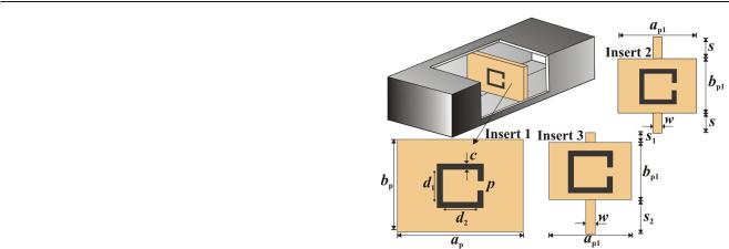
Fig. 1 3D models of the waveguide SRR using different inserts 1–3
In the following, each step of the algorithm is described. At Þrst, several models of the inserts are investigated for the optimum waveguide SRR design. SRR, in the form of the printed-circuit insert, is placed in the transverse plane of the rectangular waveguide. 3D models of those inserts are shown in Fig. 1. The main difference between the considered inserts is in the geometry of the dielectric plate. Dimensions of the printed strip of the SRR are the same for all of the inserts as follows: d1 = 2.535 mm, d2 = 2.935 mm, c = 0.2 mm,
p = 0.9 mm.
The Þrst considered insert (Insert 1) is located across the whole transverse waveguide cross section, and its dimensions are ap = 22.86 mm and bp = 10.16 mm. Insert 2 has a smaller plate with dimensions ap1 = 7 mm, bp1 = 5 mm, which is supported by two dielectric strips of equal length s = 2.58 mm, and width w = 2 mm.
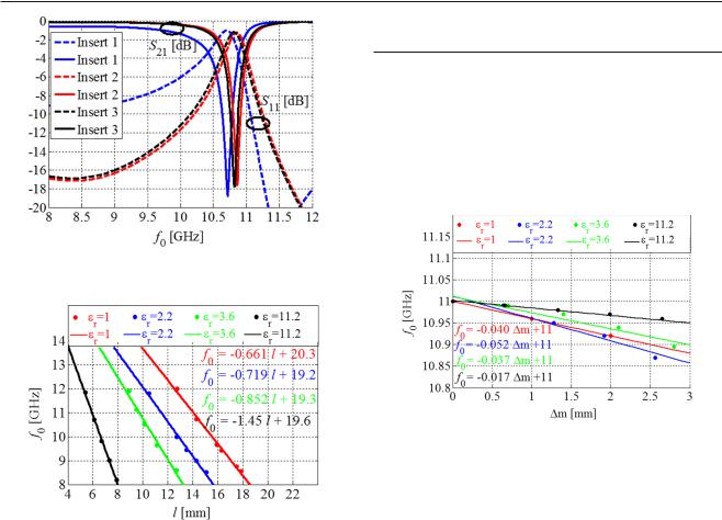
In relations to Insert 2, Insert 3 involves SRR slightly moved upwards. The dimensions of the dielectric plate remain unchanged except of the lengths of the supportive strips, which are in the case of Insert 3 s1 = 1 mm, and s2 = 4.16 mm. Frequency responses of the waveguide SRRs for different models of the inserts are presented in Fig. 2.
From Fig. 2, it can be noticed that the reduction in the dielectric plate caused the shift of the resonant frequency of the SRR toward higher values and stopband bandwidth reduction. However, moving of the SRR upwards/downwards shifted of the resonant frequency toward lower values, but the bandwidth remains unchanged.
After the choice of the insert geometry is made, the next step in the design process involves the selection of the substrate for the implementation of the Þlter. In order to investigate the effect of the strip width on the resonant frequency of the SRR, numerous analyses were performed. Considered cases included square SRR placed in air in the absence of dielectric plate to hold SRR (εr = 1) and printed on three different substrates: Rogers 5880 (εr = 2.2), Rogers 4003 (εr = 3.6), Rogers 3010 (εr = 11.2), while the thickness
123
J Comput Electron
Table 1 Relative percent error of the slope and intercept for the best linear Þt line
(%) |
εr |
= 1 |
|
εr = 2.2 |
|
εr = 3.6 |
|
εr = 11.2 |
||||
|
|
kr |
nr |
|
kr |
nr |
|
kr |
nr |
|
kr |
nr |
wI |
0 |
0 |
0 |
0.52 |
0 |
0 |
0 |
0 |
||||
wII |
0 |
0.49 |
0.14 |
0 |
0.117 |
0 |
0 |
0.512 |
||||
wIII |
0 |
0 |
0 |
0 |
0 |
0 |
0 |
0.507 |
||||
wIV |
0 |
0 |
0 |
0.52 |
0.117 |
0.52 |
0 |
0.507 |
||||
Fig. 2 Frequency responses of the waveguide SRR using different
Inserts 1–3
Fig. 3 Change of resonant frequency with total length of the SRR, with the best linear Þt to simulated data set
of the substrate is kept constant. In each of these cases, the width of the conductive strip of the SRR is varied at four different values: 0.1 mm (wI), 0.15 mm (wII), 0.20 mm (wIII), 0.25 mm (wIV). An interesting phenomena can be observed regardless of the strip width: for the same permittivity, linear relationship exists between the resonant frequency of the SRR and its total length. For the analysis performed for particular dielectric permittivity, the slopes (k) and points of intercept (n) of the obtained equations are highly similar for all of the varied widths shown in Fig. 3.
As a measure of discrepancies between the slopes and intercepts of the obtained linear equations, the percent relative error is applied. It is given by the formula:
x |
[%] |
= |
xo − xnom |
× |
100 |
(1) |
|
xnom |
|||||||
r |
|
|
|
where x0 denotes the observed value and xnom denotes the nominal value. The results for relative percent error of the slope (kr) and intercept (nr) are summarized in Table 1.
The placement of the SRR within the H -plane of the rectangular waveguide is important issue to consider in the
Fig. 4 Change of resonant frequency with the movement of the SRR toward the upper/lower waveguide wall, with the best linear Þt to simulated data set
design process. The design of the H -plane Þlter with multiple stopbands uses insert with several SRRs, so distinct stopbands are centered at the resonant frequencies of the SRRs. Such arrangement of the SRRs on the same insert implies that some SRRs are located at the distance from the center of the transverse plane of the waveguide. Therefore, the investigation of the impact of the position of the SRR on the frequency response is conducted for square SRR in air and printed on three previously used substrates: Rogers 5880 (εr = 2.2), Rogers 4003 (εr = 3.6), Rogers 3010 (εr = 11.2).
Starting from the position in the center of the transverse plane of the waveguide, the analysis was performed in two ways: Þrst, SRR is sporadically shifted toward the upper waveguide wall and then again toward the lower waveguide wall. The shift is denoted by m, and the results are given in Fig. 4 ( m = 0 mm pertains to the position of the SRR in the center of the transverse plane of the waveguide).
The Þgure shows that resonant frequency varies linearly with the movement of the SRR along the vertical waveguide axis, between the two wider waveguide walls. It is noticeable that the distance of the SRR from the center position caused a decrease in resonant frequency. An identical phenomenon happened whether the SRR is moved toward the upper/lower waveguide wall, so the obtained dependency curves are completely coinciding.
123
J Comput Electron
Fig. 6 Equivalent circuit of the waveguide SRR
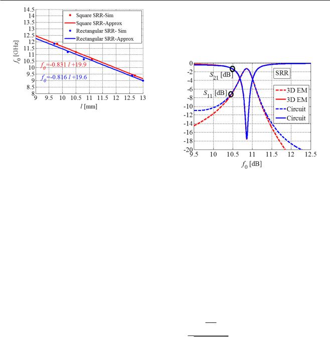
Fig. 5 Comparison between square and rectangular SRR performance: change of the resonant frequency within X-band frequency range, with the best linear Þt to simulated data set
Transformation of the square SRR to the rectangular SRR has some practical advantages. For the design of the H -plane Þlter with independently tunable stopbands, it is obligatory to eliminate the unwanted coupling between the participating SRRs. The unwanted coupling is a consequence of mutual interaction between the SRRs for different stopbands, which is caused by the proximity of the SRRs on the same insert.
An efÞcient way to distance the square SRRs on the insert, but to keep intact their resonant frequencies, is to reduce their vertical dimensions and elongate their horizontal dimensions. Such alterations actually correspond to the modiÞcation into rectangular shape. Figure 5 shows certain comparisons between the use of the square resonator and rectangular one having the same resonant frequency. To obtain the rectangular SRR, adjacent sides of the square SRR were simultaneously varied. Resonant frequency for both, the square and rectangular SRR, varies linearly with the total length of the resonator. Also, it can be perceived that for the particular resonant frequency, square-shaped SRR exhibits greater total length compared to the rectangular SRR.
Based on the above results, it can be outlined that the resonant frequency of the SRR and considered design parameters can be related by:
f0 [GHz] = k × i [mm] + n |
(2) |
where parameter i refers to the total length of the SRR or its movement along the waveguide cross section, depending on the considered case.
2.2 Equivalent electrical circuit of the waveguide SRR
An equivalent electrical circuit of the SRR (implemented as Insert 2) is a parallel resonant circuit, and it is shown in Fig. 6.
Fig. 7 Comparison of frequency responses for the 3D EM model of the SRR and its equivalent electrical circuit
Values of the elements of the equivalent circuit were found by using the following equations:
R = |
2 |S11 ( jω0)| Z0 |
|
(1 − |S11 ( jω0)|) |
(3) |
||||
L |
= |
2B3dB |
| |
S11 ( jω0) |
| |
Z0 ω2 |
(4) |
|
|
|
|
|
0 |
|
|||
C = |
1 (2B3dB |S11 ( jω0)| Z0) |
(5) |
||||||
where ω0 is angular frequency in [rad/s], B3dB is 3 dB bandwidth (rad/s) and S11 (jω0) is the value of the S11 parameter at the considered resonant frequency. Z0 refers to the wave impedance for the dominant mode of the waveguide at particular frequency f , given by the formula:
|
|
μ ε |
|
Z0 = 1 − fc f 2 |
(6) |
where fc designates the cutoff frequency of the waveguide, while parameters μ and ε denote the permeability and the permittivity of the medium, respectively. For the considered resonant frequency f0 = 10.90 GHz, the wave impedance has the value equal to 472 . Accordingly, port impedances are set to correspond to Z0. Waveguide section of length D0 = 4 mm represents the distance of the SRR to the waveguide ports. The values of the circuit elements are as follows: R = 6262 , L = 0.429 nH, C = 0.497 pF. Comparison of frequency responses of the 3D EM model and equivalent circuit is shown in Fig. 7.
123
J Comput Electron
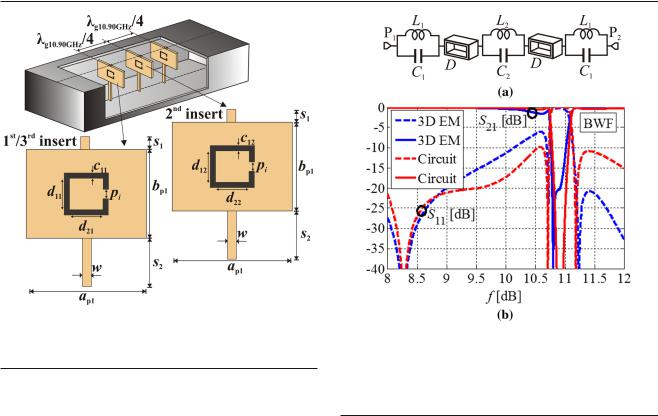
Fig. 8 3D model of BWF using SRR
Table 2 Dimensions of SRRs and inserts used for the design of BWF
Resonating insert |
d1i (mm) |
d2i (mm) |
c1i |
(mm) |
pi (mm) |
1st/3rd (i = 1, 3) |
2 |
3.25 |
0.25 |
0.9 |
|
2nd (i = 2) |
2 |
3.25 |
0.2 |
|
0.9 |
Size (mm) |
ap1 |
bp1 |
s1 |
s2 |
w |
|
7 |
4 |
1 |
5.16 |
2 |
|
|
|
|
|
|
Fig. 9 a Equivalent electrical circuit of the third-order BWF. b Comparison of the frequency responses for the 3D EM model and the equivalent electrical circuit
Table 3 Values of circuit elements for BWF
Parameter |
L1 (nH) |
L2 (nH) |
C1 (pF) |
C2 (pF) |
Value |
0.342 |
0.331 |
0.624 |
0.634 |
|
|
|
|
|
3 Third-order bandstop waveguide Þlter (BWF) using SRRs
In this section, the third-order BWF based on the use of SRRs is presented. Center frequency of the stopband is f0 = 10.90 GHz, and bandwidth B3dB = 340 MHz. 3D model of BWF is shown in Fig. 8.
The Þlter is designed using SRRs in the form of the H- plane inserts placed within rectangular waveguide. These inserts are mutually separated by the waveguide section of length of λg10.90GHz/4 = 8.615 mm, to implement the quarter-wave inverters for the considered center frequency. Dimensions of the used SRRs are collected in Table 2.
3.1 Equivalent electrical circuit of BWF
Equivalent electrical circuit of the third-order BWF is shown in Fig. 9a. In the presented circuit, the losses are not taken into account. Values of the circuit elements are calculated using Eqs. 4 and 5 and given in Table 3.
SRRs are modeled by the parallel resonant circuits that are mutually separated by the waveguide section of length D, to realize the quarter-wave transformer for the corre-
sponding resonant frequency. In the considered case, D =
λg10.90GHz/4 = 8.615 mm.
Comparison of the frequency responses for the 3D EM model of BWF and its equivalent circuit is presented in Fig. 9b. A good agreement between the results is observed in terms of the center frequency of the Þlter and bandwidth.
4 Dual-band bandstop waveguide Þlter (DBBWF) using SRRs
In this section, the design and strategy for the miniaturization of DBBWF are discussed. The concept of miniaturization relies on replacement of the conventional quarter-wave inverter with the shorter one.
The usefulness of the proposed design is veriÞed by example of the third-order H -plane compact DBBWF (CDBBWF). Both Þlters, DBBWF and CDBBWF, are designed to meet the same speciÞcation. Two distinct stopbands are centered at frequencies f01 = 8.90 GHz (Band I) and f02 = 10.90 GHz (Band II), featuring equal bandwidths B3dB1 = B3dB2 = 340 MHz. Subsequently, comparisons between DBBWF and CDBBWF are exposed.
123